Module: TRM Name always "TE Series Name" +TRM Example: "TE0728 TRM"
Carrier: TRM Name usually "TEB Series Name" +TRM Example: "TEB0728 TRM"
HTML
<!-- tables have all same width (web max 1200px and pdf full page(640px), flexible width or fix width on menu for single column can be used as before) -->
<style>
.wrapped{
  width: 100% !important;
  max-width: 1200px !important;
 }
</style>
Page properties
hidden
true
id
Comments
Important General Note:
If some section is configurable and depends on Firmware, please refer to the addition page (for example CPLD). If not available, add note, that this part is configurable
Designate all graphics and pictures with a number and a description, Use "Scroll Title" macro
Use "Scroll Title" macro for pictures and table labels. Figure number must be set manually at the moment (automatically enumeration is planned by scrollPDF)
Figure template:
Scroll Title
anchor
Figure_anchorname
title
Text
Scroll Ignore
Create DrawIO object here: Attention if you copy from other page, objects are only linked.
Scroll Only
image link to the generate DrawIO PNG file of this page. This is a workaround until scroll pdf export bug is fixed
Table template:
Layout macro can be use for landscape of large tables
Scroll Title
anchor
Table_tablename
title
Text
Scroll Table Layout
orientation
portrait
sortDirection
ASC
repeatTableHeaders
default
style
widths
sortByColumn
1
sortEnabled
false
cellHighlighting
true
Example
Comment
1
2
The anchors of the Scroll Title should be named consistant across TRMs. A incomplete list of examples is given below
<type>_<main section>_<name>
type: Figure, Table
main section:
"OV" for Overview
"SIP" for Signal Interfaces and Pins,
"OBP" for On board Peripherals,
"PWR" for Power and Power-On Sequence,
"B2B" for Board to Board Connector,
"TS" for Technical Specification
"VCP" for Variants Currently in Production
"RH" for Revision History
name: custom, some fix names, see below
Fix names:
"Figure_OV_BD" for Block Diagram
"Figure_OV_MC" for Main Components
"Table_OV_IDS" for Initial Delivery State
"Table_PWR_PC" for Power Consumption
"Figure_PWR_PD" for Power Distribution
"Figure_PWR_PS" for Power Sequence
"Figure_PWR_PM" for Power Monitoring
"Table_PWR_PR" for Power Rails
"Table_PWR_BV" for Bank Voltages
"Table_TS_AMR" for Absolute_Maximum_Ratings
"Table_TS_ROC" for Recommended_Operating_Conditions
"Figure_TS_PD" for Physical_Dimensions
"Table_VCP_SO" for TE_Shop_Overview
"Table_RH_HRH" for Hardware_Revision_History
"Figure_RH_HRN" for Hardware_Revision_Number
"Table_RH_DCH" for Document_Change_History
Use Anchor in the document: add link macro and add "#<anchorname>
Refer to Anchror from external : <page url>#<pagename without space characters>-<anchorname>
The Trenz Electronic TEB0724-02 is a developement carrier board for the TE0724 and compatible modules. It facilitates easy access to all on the module available features.
Refer to http://trenz.org/teb0724-info for the current online version of this manual and other available documentation.
2x10 Pin header for Boot and Programming options, J6
2x6 Pin header for jumper setting of CAN bus termination resistors, J22
microSD Card Slot, J5
Dip switches for selecting B_VCCIO_35, S6
DCDC (B_VCCIO_35), U8
DCDC (B_3.3V), U7
Initial Delivery State
Page properties
hidden
true
id
Comments
Note
Only components like EEPROM, QSPI flash and DDR3 can be initialized by default at manufacture.
If there is no components which might have initial data ( possible on carrier) you must keep the table empty
Scroll Title
anchor
Table_OV_IDS
title
Initial delivery state of programmable devices on the module.
Scroll Table Layout
orientation
portrait
sortDirection
ASC
repeatTableHeaders
default
style
widths
sortByColumn
1
sortEnabled
false
cellHighlighting
true
Storage device name
Content
Notes
FTDI Configuration EEPROM U3
Xilinx License
Do not overwrite, see warning in related section
Configuration Signals
Page properties
hidden
true
id
Comments
Overview of Boot Mode, Reset, Enables,
The boot device is selected by the mode jumpers on pin header J6. Placing a jumper at pin 13-14 sets Mode0 to low level. Mode1 is set to low level by jumper on pin 15-16. Boot modes are further described at the corresponding section of the modules, e.g. Table 2, Boot mode selection of TE0724 TRM. Default with no jumpers is boot from SD-Card.
Scroll Title
anchor
Table_OV_BP
title
Boot process.
Scroll Table Layout
orientation
portrait
sortDirection
ASC
repeatTableHeaders
default
style
widths
sortByColumn
1
sortEnabled
false
cellHighlighting
true
Signal
Function
Routed to
B2B Connector Pin
Note
Mode0
bootdevice selection
jumper pins J6-13 J6-14
J1-4
TE0724: pulled up at module
Mode1
bootdevice selection
jumper pins J6-15 J6-16
J1-2
TE0724: pulled up at module
ONKEY
module power signal
push button S1 and pin J6-9
J1-148
TE0724: pulled up at module
RESETREQ
module reset
push button S3 and pin J6-12
J1-150
TE0724: pulled up at module
PWR_GPIO2
-
J6-8
J1-143
User power sequenzing IO
PWR_GPIO4
-
J6-10
J1-141
User power sequenzing IO
Signals, Interfaces and Pins
Page properties
hidden
true
id
Comments
Notes :
For carrier or stand-alone boards use subsection for every connector typ (add designator on description, not on the subsection title), for example:
SD
USB
ETH
FMC
...
For modules which needs carrier us only classes and refer to B2B connector if more than one is used, for example
JTAG
UART
I2C
MGT
...
Board to Board (B2B) I/Os
I/O signals connected to the B2B connector:
Scroll Title
anchor
Table_SIP_B2B
title
General overview of PL I/O signals and SoM's interfaces connected to the B2B connectors
Scroll Table Layout
orientation
portrait
sortDirection
ASC
repeatTableHeaders
default
style
widths
sortByColumn
1
sortEnabled
false
cellHighlighting
true
B2B Connector
Interfaces
I/O Signal Count
Notes
J1
User IO
72 single ended or 36 differential
9x Pmod
6 LED
red
2 Push Button
-
7 MIO
J7 (not assembled), TE0724: 3.3V
2 MIO
J9 (not assembled), TE0724: 1.8V
1 MIO LED
green
1 MIO Push Button
-
I²C
2
1x Pmod
SD IO
7
-
UART
2
-
CAN
2
-
GbE PHY_MDIO + PHY_LEDs
10
-
JTAG
4
-
Power GPIO
2
-
Power/Reset/Fuse programming
3
-
Bootmode
2
-
microUSB JTAG/UART Interface
The microUSB connector provides JTAG access to the module through the carriers USB to JTAG/UART bridge, routed to B2B connector J1. The UART is routed via a levelshifter. There is no device with JTAG port on the baseboard.
Scroll Title
anchor
Table_SIP_JTG
title
JTAG pins connection
Scroll Table Layout
orientation
portrait
sortDirection
ASC
repeatTableHeaders
default
style
widths
sortByColumn
1
sortEnabled
false
cellHighlighting
true
Signal
B2B Connector Pin
TCK
J1-147
TDI
J1-151
TDO
J1-145
TMS
J1-149
UART RX
J1-36
UART TX
J1-38
SD Card Interface
Scroll Title
anchor
Table_SIP_SDC
title
SD Card interface signals and connections
Scroll Table Layout
orientation
portrait
sortDirection
ASC
repeatTableHeaders
default
style
widths
sortByColumn
1
sortEnabled
false
cellHighlighting
true
Connected To
Signal Name
Notes
J1-34
SD-CD
Card detect switch, pulled up, low if card inserted.
J1-24
SD-D0
J1-22
SD-CMD
J1-20
SD-CCLK
J1-26
SD-D1
J1-28
SD-D2
J1-30
SD-D3
Ethernet Interface
The TEB0724 Carrier Board has a RJ45 Gigabit Ethernet MagJack (J3) with two LEDs. On-board Ethernet MagJack pins are routed to B2B connector J1 via MDI. LEDs are also routed to the B2B connector.
Ethernet PHY connection
Scroll Title
anchor
Table_SIP_ETH
title
Ethernet Signals
Scroll Table Layout
orientation
portrait
sortDirection
ASC
repeatTableHeaders
default
style
widths
sortByColumn
1
sortEnabled
false
cellHighlighting
true
MagJack
Signal
B2B
J3-2
PHY_MDI0_P
J1-7
J3-3
PHY_MDI0_N
J1-9
J3-4
PHY_MDI1_P
J1-13
J3-5
PHY_MDI1_N
J1-15
J3-6
PHY_MDI2_P
J1-19
J3-7
PHY_MDI2_N
J1-21
J3-8
PHY_MDI3_P
J1-25
J3-9
PHY_MDI3_N
J1-27
J3B
PHY_LED0
J1-10
J3C
PHY_LED1
J1-12
I2C Interface
On-board I2C bus is accaessable with the following pins:
Scroll Title
anchor
Table_SIP_I2C
title
I2C pins
Scroll Table Layout
orientation
portrait
sortDirection
ASC
repeatTableHeaders
default
style
widths
sortByColumn
1
sortEnabled
false
cellHighlighting
true
SDA
SCL
Notes
J1-144
J1-142
B2B
J6-7
J6-5
In-Circuit Programming
J21-10, J21-4
J21-9, J21-3
Pmod
There are no I2C devices on the base board. Pullup resistors have to be provided by the module.
Pmods
The GPIOs of the 10 Pmods (J10 to J17, J20, J21) are connected with 100 Ohm differential routing to the B2B connector. J21 is a pure I2C compatible Pmod, without additional signals. The other 9 are GPIO Pmods where despite J20 all others can be used as dual Pmods.
Via dip switsches S6-1 to S6-3the variable bank power B_VCCIO_35 for the Pmods J10, J11, J12, J13, J14, J16 can be selected. Respect power regulator limits!
Scroll Title
anchor
Table_OBP_PMD
title
Pmod connections.
Scroll Table Layout
orientation
portrait
sortDirection
ASC
repeatTableHeaders
default
style
widths
sortByColumn
1
sortEnabled
false
cellHighlighting
true
J10
J11
J12
J13
J14
PIN
Signal
B2B
Signal
B2B
Signal
B2B
Signal
B2B
Signal
B2B
1
PA0_P
J1-56
PB2_N
J1-70
PC2_P
J1-57
PD2_P
J1-77
PE2_N
J1-90
2
PA0_N
J1-58
PB2_P
J1-72
PC2_N
J1-55
PD2_N
J1-75
PE2_P
J1-92
3
PA3_P
J1-46
PB0_N
J1-76
PC0_P
J1-51
PD0_P
J1-71
PE0_N
J1-96
4
PA3_N
J1-48
PB0_P
J1-78
PC0_N
J1-49
PD0_N
J1-69
PE0_P
J1-98
5
GND
-
GND
-
GND
-
GND
-
GND
-
6
VCCIO_35
J1-54
VCCIO_35
J1-54
VCCIO_35
J1-54
VCCIO_35
J1-54
VCCIO_35
J1-54
7
PA1_N
J1-62
PB3_P
J1-68
PC3_N
J1-59
PD3_N
J1-79
PE3_P
J1-88
8
PA1_P
J1-60
PB3_N
J1-66
PC3_P
J1-61
PD3_P
J1-81
PE3_N
J1-86
9
PA2_N
J1-52
PB1_P
J1-82
PC1_N
J1-45
PD1_N
J1-65
PE1_P
J1-102
10
PA2_P
J1-50
PB1_N
J1-80
PC1_P
J1-47
PD1_P
J1-67
PE1_N
J1-100
11
GND
-
GND
-
GND
-
GND
-
GND
-
12
B_VCCIO_35
J1-54
B_VCCIO_35
J1-54
B_VCCIO_35
J1-54
B_VCCIO_35
J1-54
B_VCCIO_35
J1-54
J15
J16
J17
J20
J21
PIN
Signal
B2B
Signal
B2B
Signal
B2B
Signal
B2B
Signal
B2B
1
PG2_N
J1-110
PF2_P
J1-97
PH2_P
J1-115
PI2_P
J1-133
NC
-
2
PG2_P
J1-112
PF2_N
J1-95
PH2_N
J1-113
PI2_N
J1-131
NC
-
3
PG0_P
J1-114
PF0_P
J1-91
PH0_P
J1-111
PI0_P
J1-129
I2C_SCL
J1-142
4
PG0_N
J1-116
PF0_N
J1-89
PH0_N
J1-109
PI0_N
J1-127
I2C_SDA
J1-144
5
GND
-
GND
-
GND
-
GND
-
GND
-
6
3.3V
J1-74, J1- 43
VCCIO_35
J1-54
3.3V
J1-74, J1- 43
3.3V
J1-74, J1- 43
3.3V
J1-74, J1- 43
7
PG3_P
J1-108
PF3_N
J1-99
PH3_N
J1-117
PI3_N
J1-135
NC
-
8
PG3_N
J1-106
PF3_P
J1-101
PH3_P
J1-119
PI3_P
J1-137
NC
-
9
PG1_N
J1-120
PF1_N
J1-85
PH1_N
J1-105
PI1_N
J1-123
I2C_SCL
J1-142
10
PG1_P
J1-121
PF1_P
J1-87
PH1_P
J1-107
PI1_P
J1-125
I2C_SDA
J1-144
11
GND
-
GND
-
GND
-
GND
-
GND
-
12
3.3V
J1-74, J1- 43
B_VCCIO_35
J1-54
3.3V
J1-74, J1- 43
3.3V
J1-74, J1- 43
3.3V
J1-74, J1- 43
CAN Screw Terminal
The CAN bus is routed to screw terminal J2.
Scroll Title
anchor
Table_OBP_CAN
title
CAN bus connection
Scroll Table Layout
orientation
portrait
sortDirection
ASC
repeatTableHeaders
default
style
widths
sortByColumn
1
sortEnabled
false
cellHighlighting
true
PIN
Signal
B2B
J2-1
CAN0_N
J1-1
J2-2
GND
J2-3
CAN0_P
J1-3
Jumpers on J22-1 to J22-3 and J22-2 to J22-4 connect proper split termination resistors to the CAN bus.
Pin Header
Pin Header J6 provides access to power functions, bootmode selection and PMIC In-Circuit Programming (For initial PMIC In-Circuit Programming of the module, Diode D28 has to be removed).
Scroll Title
anchor
Table_OBP_PHJ6
title
Pin Header J6
Scroll Table Layout
orientation
portrait
sortDirection
ASC
repeatTableHeaders
default
style
widths
sortByColumn
1
sortEnabled
false
cellHighlighting
true
PIN
Signal
B2B
J6-1
VIN
J1-154, J1-156, J1-158, J1-160
J6-2
VIN
J1-154, J1-156, J1-158, J1-160
J6-3
GND
J6-4
GND
J6-5
I2C_SCL
J1-142
J6-6
VBAT
J1-152
J6-7
I2C_SDA
J1-144
J6-8
PWR_GPIO2
J1-143
J6-9
ONKEY
J1-148
J6-10
PWR_GPIO4
J1-141
J6-11
PWR_TP
J1-146
J6-12
RESETREQ
J1-150
J6-13
MODE0
J1-2
J6-14
GND
J6-15
MODE1
J1-4
J6-16
GND
Alternatively to selecting B_VCCIO_35 by using S6 dip switches, VCCIO_35 ( e.g. SoM TE0724, Bank 35) can be selected by removing R45 and adding a jumper on optional J19. In table 18 valid jumper positions are given. Voltages and maximum current ratings could be found in the corresponding TRM of the attached module, (e.g. TE0724 TRM#PowerRails ).
Scroll Title
anchor
Table_OBP_PHJ19
title
Optional Pin Header J19
Scroll Table Layout
orientation
portrait
sortDirection
ASC
repeatTableHeaders
default
style
widths
sortByColumn
1
sortEnabled
false
cellHighlighting
true
PIN
Signal
B2B
J19-1
VLDO1
J1-83
J19-2
GND
J19-3
VCCIO_35
J1-54
J19-4
VLDO2
J1-94
J19-5
VLDO34
J1-53
J19-6
GND
Scroll Title
anchor
Table_OBP_VSJ19
title
J19 Jumper settings for VCCIO_35 voltage selection
Scroll Table Layout
orientation
portrait
sortDirection
ASC
repeatTableHeaders
default
style
widths
sortByColumn
1
sortEnabled
false
cellHighlighting
true
Jumper position
Signal
e.g. TE0724
draw.io Diagram
border
false
viewerToolbar
true
fitWindow
false
diagramDisplayName
lbox
true
revision
3
diagramName
Jumper_Settings_J19_5-3_TEB0724
simpleViewer
true
width
200
links
auto
tbstyle
top
diagramWidth
293
J19 1-3
VLDO1
3.3V
draw.io Diagram
border
false
viewerToolbar
true
fitWindow
false
diagramDisplayName
lbox
true
revision
5
diagramName
Jumper_Settings_J19_TEB0724
simpleViewer
true
width
200
links
auto
tbstyle
top
diagramWidth
293
J19 4-3
VLDO2
1,8V
draw.io Diagram
border
false
viewerToolbar
true
fitWindow
false
diagramDisplayName
lbox
true
revision
3
diagramName
Jumper_Settings_J19_4-3_TEB0724
simpleViewer
true
width
200
links
auto
tbstyle
top
diagramWidth
293
J19 5-3
VLDO34
2,5V
Warning
Respect VLDO current limitations!
Optional fitted headers J7, J8 and J9 are to provide full access to the Pins at the B2B connector, especially for testing and extension purposes. Description follows below.
PL Button and LED IOs are additionally routed to optionally assembled pin header J8.
Scroll Title
anchor
Table_OBP_PHJ8
title
Optional Pin Header J8
Scroll Table Layout
orientation
portrait
sortDirection
ASC
repeatTableHeaders
default
style
widths
sortByColumn
1
sortEnabled
false
cellHighlighting
true
PIN
Signal
B2B
J8-1
3.3V
J1-43, J1-74
J8-2
GND
J8-3
S4
J1-126
J8-4
S2
J1-124
J8-5
ULED5
J1-130
J8-6
ULED6
J1-128
J8-7
ULED3
J1-134
J8-8
ULED4
J1-132
J8-9
ULED1
J1-138
J8-10
ULED2
J1-136
Optional pin header J7 gives access to otherwise not used PS MIO IOs at a 3.3V bank.
Scroll Title
anchor
Table_OBP_PHJ7
title
Optional Pin Header J7
Scroll Table Layout
orientation
portrait
sortDirection
ASC
repeatTableHeaders
default
style
widths
sortByColumn
1
sortEnabled
false
cellHighlighting
true
PIN
Signal
B2B
J7-1
3.3V
43, 74
J7-2
GND
J7-3
GND
J7-4
MIO8
J1-14
J7-5
MIO10
J1-31
J7-6
MIO11
J1-33
J7-7
MIO12
J1-35
J7-8
MIO13
J1-37
J7-9
MIO14
J1-39
J7-10
MIO15
J1-41
Optional pin header J9 gives access to otherwise not used PS MIO IOs at a 1.8V bank.
Scroll Title
anchor
Table_OBP_PHJ9
title
Optional Pin Header J9.
Scroll Table Layout
orientation
portrait
sortDirection
ASC
repeatTableHeaders
default
style
widths
sortByColumn
1
sortEnabled
false
cellHighlighting
true
PIN
Signal
B2B
J9-1
1.8V
J1-63
J9-2
GND
J9-3
GND
J9-4
MIO_46
J1-32
J9-5
MIO_50
J1-40
J9-6
MIO_PB
J1-42
On-board Peripherals
HTML
<!--
Components on the Module, like Flash, PLL, PHY...
  -->
USB to JTAG/UART bridge
The TEB0724 carrier board has on-board microUSB 2.0 (J4) high-speed to UART/FIFO IC FT2232H (U1) from FTDI. Channel A can be used as JTAG Interface (MPSSE) to program on module JTAG devices. Channel B can be used as UART Interface routed via a level shifter to the 1.8V section of the B2B connector, usually connected to the PS of the SoM. There is also a 256-byte serial EEPROM connected to the FT2232H chip pre-programmed with license code to support Xilinx programming tools.
Warning
Do not access the FT2232H EEPROM using FTDI programming tools, doing so will erase normally invisible user EEPROM content and invalidate stored Xilinx JTAG license. Without this license the on-board JTAG will not be accessible any more with any Xilinx tools. Software tools from FTDI website do not warn or ask for confirmation before erasing user EEPROM content.
Oscillators
The module has the following reference clock signals provided by on-board oscillators:
Scroll Title
anchor
Table_OBP_CLK
title
Reference clock signals
Scroll Table Layout
orientation
portrait
sortDirection
ASC
repeatTableHeaders
default
style
widths
sortByColumn
1
sortEnabled
false
cellHighlighting
true
Clock Source
Schematic Name
Frequency
Clock Destination
SiTime SiT8008AI oscillator, U4
OSCI
12.000000 MHz
U1, pin 3.
On-board LEDs
Scroll Title
anchor
Table_OBP_LED
title
On-board LEDs
Scroll Table Layout
orientation
portrait
sortDirection
ASC
repeatTableHeaders
default
style
widths
sortByColumn
1
sortEnabled
false
cellHighlighting
true
LED
Color
Signal
Description and Notes
D1
green
VIN
power indicator
D2-D7
red
ULED1..6
User LED
D8
green
MIO9
MIO user LED
J3B
green
PHY_LED0
Ethernet status
J3C
yellow
PHY_LED1
Ethernet status
On-board Push Buttons
Scroll Title
anchor
Table_OBP_PB
title
On-board Push Button
Scroll Table Layout
orientation
portrait
sortDirection
ASC
repeatTableHeaders
default
style
widths
sortByColumn
1
sortEnabled
false
cellHighlighting
true
Button
Signal
B2B
Description and Notes
S1
ONKEY
J1-148
Power Button, pulled up, on push de-asserted
S3
RESETREQ
J1-150
User LED pulled up, on push de-asserted
S2
S2
J1-124
PL user button, pulled up, on push de-asserted
S4
S4
J1-126
PL user button, pulled up, on push de-asserted
S5
MIO51
J1-42
PS MIO user button, pulled up, on push de-asserted
Dip-Switches
Dip-switch S6-1..3 are used to select the adjustable board power. Tabel 14 shows the signals, table 15 how to adjust the switches for corresponding B_VCCIO_35 Voltages.
Scroll Title
anchor
Table_OBP_DIS
title
Dip-Switches
Scroll Table Layout
orientation
portrait
sortDirection
ASC
repeatTableHeaders
default
style
widths
sortByColumn
1
sortEnabled
false
cellHighlighting
true
Switch
Signal
S6-1
VADJ_VS0
S6-2
VADJ_VS1
S6-3
VADJ_VS2
S6-4
NC
Scroll Title
anchor
Table_OBP_DSS
title
Select B_VCCIO_35 via Dip-Switches.
Scroll Table Layout
orientation
portrait
sortDirection
ASC
repeatTableHeaders
default
style
widths
sortByColumn
1
sortEnabled
false
cellHighlighting
true
B_VCCIO_35
S6-1
S6-2
S6-3
3.3V
ON
ON
ON
2.5V
OFF
ON
ON
1.8V
ON
OFF
ON
1.5V
OFF
OFF
ON
1.25V
ON
ON
OFF
1.2V
OFF
ON
OFF
Power and Power-On Sequence
Page properties
hidden
true
id
Comments
In 'Power and Power-on Sequence' section there are three important digrams which must be drawn:
Power on-sequence
Power distribution
Voltage monitoring circuit
Note
For more information regarding how to draw diagram, Please refer to "Diagram Drawing Guidline" .
Power Consumption
Power supply with minimum current capability of 3A for system startup is recommended.
The maximum power consumption depends on the attached module the design running on the module and additional peripherals.
Xilinx provide a power estimator excel sheets to calculate power consumption for FPGAs. It's also possible to evaluate the power consumption of the developed design with Vivado. See also Trenz Electronic Wiki FAQ.
Scroll Title
anchor
Table_PWR_PC
title
Power Consumption
Scroll Table Layout
orientation
portrait
sortDirection
ASC
repeatTableHeaders
default
style
widths
sortByColumn
1
sortEnabled
false
cellHighlighting
true
Power Input
Typical Current
VIN
340 mA
Warning
To avoid any damage to the base board and attached module, check for stabilized voltages should be carried out (i.e. power good and enable signals) before powering up any SoC's I/O bank voltages VCCO_x. All I/Os should be tri-stated during power-on sequence.
Power Distribution Dependencies
Scroll Title
anchor
Figure_PWR_PD
title
Power Distribution
Scroll Ignore
draw.io Diagram
border
false
viewerToolbar
true
fitWindow
false
diagramDisplayName
lbox
true
revision
6
diagramName
PD_TEB0724
simpleViewer
true
width
links
auto
tbstyle
top
diagramWidth
641
Scroll Only
User should also check related module documentation and Xilinx data sheet, respectively.
Power-On Sequence
The power-on sequence is solely controlled by the attached module. The baseboard DCDC regulators U7 and U8 are enabled by the 3.3V rail of the module. Optional sequenzing signals for integration of additional hardware are PWR_GPIO2 and PWR_GPIO4.
If the attached module uses an external bank power VCCIO_35, this has to be powered up after the modules SOCs powerrails are up and before any other signal is applied to the bank IOs. The 1.8V and 3.3V power rails are used for the SD Card level shifter U13. The datasheet states to first power up 1.8V and then 3.3V, this has to be taken into account when reconfiguring the power circuit of the attached SoM.
Power-Off is in reverse order. VCCIO_35 has to be disabled before the SoCs core voltages are turned off.
Power Rails
Some of the power rails are sourced by the attached module, see coresponding TRMs of this for further information (e.g. TE0724 TRM#PowerRails).
Scroll Title
anchor
Table_PWR_PR
title
Board power rails.
Scroll Table Layout
orientation
portrait
sortDirection
ASC
repeatTableHeaders
default
style
widths
sortByColumn
1
sortEnabled
false
cellHighlighting
true
Power Rail Name
B2B J1 Pins
Direction on B2B
Notes
VIN
154, 156, 158, 160
Output
External main supply voltage (5V).
B_3.3V
-
-
Onboard DCDC.
B_VCCIO_35
-
-
Onboard adjustable DCDC.
3.3V
43, 74
Input
1.8V
63
Input
VCCIO_35
54
Output
Connected via 0Ohm R45 to B_VCCIO_35 or source selectable by J19 (R45 removed).
VLDO1
83
Input
(TE0724: 3.3V)
VLDO2
94
Input
Used to enable UART level shifter. Therefore fix at 1.8V.
VLDO34
53
Input
(TE0724: 2.5V)
VBAT
152
Input/Output
Reserved for PMIC backup battery and charger.
Board to Board Connectors
Page properties
hidden
true
id
Comments
This section is optional and only for modules.
use "include page" macro and link to the general B2B connector page of the module series, for example: 4 x 5 SoM LSHM B2B Connectors
Include Page
4 x 6 SoM SS5/ST5 B2B Connectors
4 x 6 SoM SS5/ST5 B2B Connectors
Technical Specifications
Absolute Maximum Ratings
Page properties
hidden
true
id
Comments
Note
Only user configurable signals must be mentioned in 'Absolute Maximum Rating' and 'Recommended Operating Conditions'. Please avoid to mention all maximum rating for all components.
Scroll Title
anchor
Table_TS_AMR
title
Board absolute maximum ratings.
Scroll Table Layout
orientation
portrait
sortDirection
ASC
repeatTableHeaders
default
style
widths
sortByColumn
1
sortEnabled
false
cellHighlighting
true
Parameter
Min
Max
Units
Reference Document
VIN supply voltage
-0.3
5.5
V
Depends mostly on attached SoM, values here are for TE0724 PMIC, da9062_3v4.pdf.
Storage temperature
-30
80
°C
Push buttons datasheet.
Note
Assembly variants for higher storage temperature range are available on request.
Recommended Operating Conditions
Scroll Title
anchor
Table_TS_AMR
title
Recommended Operating Conditions.
Scroll Table Layout
orientation
portrait
sortDirection
ASC
repeatTableHeaders
default
style
widths
sortByColumn
1
sortEnabled
false
cellHighlighting
true
Parameter
Min
Max
Units
Reference Document
VIN supply voltage
0
5.5
V
Depends mostly on attached SoM, values here are for TE0724 PMIC, da9062_3v4.pdf.
Operating temperature
-25
70
°C
Push buttons datasheet.
Note
Please check also the attached SOMs datasheet for a complete list of absolute maximum and recommended operating ratings.
Operating temperature range depends also on customer design and cooling solution. Please contact us for options.
Physical Dimensions
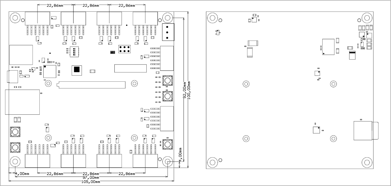
Module size: 105 mm × 100 mm. Please download the assembly diagram for exact numbers.
Mating height with standard connectors: 4 mm.
PCB thickness: 1.6 mm.
Highest part on PCB: approx. 13.5 mm. Please download the step model for exact numbers.
Page properties
hidden
true
id
Comments
In 'Physical Dimension' section, top and button view of moduloe must be insterted, information regarding physical dimention can be obtained through webpage for product in Shop.Trenz, (Download> Documents> Assembly part)for every SoM.
For Example: for Module TE0728, Physical Dimension information can be captured by snipping tools from the link below:
Hardware revision number can be found on the PCB board together with the module model number separated by the dash.
Scroll Title
anchor
Figure_RH_HRN
title
Hardware Revision Number.
Document Change History
Page properties
hidden
true
id
Comments
Note this list must be only updated, if the document is online on public doc!
It's semi automatically, so do following
Add new row below first
Copy "Page Information Macro(date)" Macro-Preview, Metadata Version number, Author Name and description to the empty row. Important Revision number must be the same as the Wiki document revision number Update Metadata = "Page Information Macro (current-version)" Preview+1 and add Author and change description. --> this point is will be deleted on newer pdf export template
Metadata is only used of compatibility of older exports
Scroll Title
anchor
Table_RH_DCH
title
Document change history.
Scroll Table Layout
orientation
portrait
sortDirection
ASC
repeatTableHeaders
default
style
widths
sortByColumn
1
sortEnabled
false
cellHighlighting
true
Date
Revision
Contributors
Description
Page info
modified-date
modified-date
dateFormat
yyyy-MM-dd
Page info
infoType
Current version
dateFormat
yyyy-MM-dd
prefix
v.
type
Flat
Page info
infoType
Modified by
dateFormat
yyyy-MM-dd
type
Flat
Update to TRM 2.4 style
Corrected Table 15
Added Comment on Module PMIC in Circuit Programming
v.31
Martin Rohrmüller
Splitted table 9 in two parts
v.30
Martin Rohrmüller
Update to REV02
Two DCDCs added, changes in the entire document
v.29
Martin Rohrmüller
Added Figure J19 Jumper settings
updated Table counter
v.28
Martin Rohrmüller
Updated assembly pictures
Added typical power consumption
Added hints on power rail voltages
v.27
Martin Rohrmüller
Updated link to TE0724
v.26
Martin Rohrmüller
Changed VCCIO_35 connection: R45 not placed , J19 placed