...
| Scroll Title |
|---|
| anchor | Figure_OV_BD |
|---|
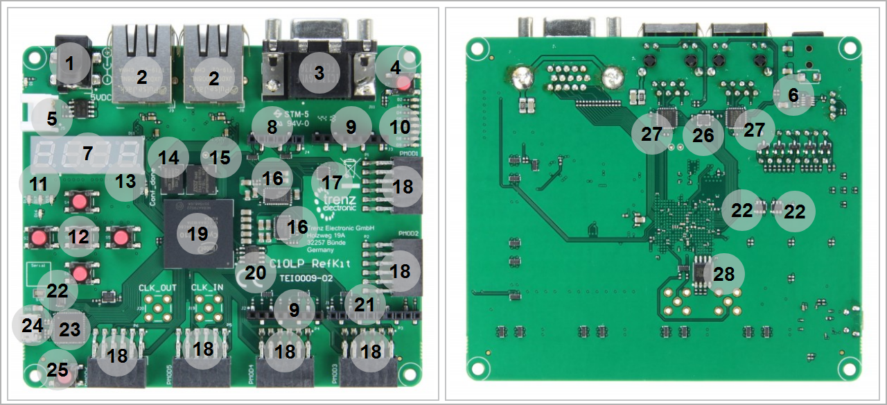
| title | TExxxx TEI0009 main components |
|---|
|
| Scroll Ignore |
|---|
| draw.io Diagram |
|---|
| border | false |
|---|
| viewerToolbar | true |
|---|
| |
|---|
| fitWindow | false |
|---|
| diagramDisplayName | |
|---|
| lbox | true |
|---|
| revision | 4 |
|---|
| diagramName | TEI0009_OV_MC |
|---|
| simpleViewer | false |
|---|
| width | |
|---|
| links | auto |
|---|
| tbstyle | hidden |
|---|
| diagramWidth | 640 |
|---|
|
|
| Scroll Only |
|---|
|
|
...
| Scroll Title |
|---|
| anchor | Table_OV_IDS |
|---|
| title | Initial delivery state of programmable devices on the module |
|---|
|
| Scroll Table Layout |
|---|
| orientation | portrait |
|---|
| sortDirection | ASC |
|---|
| repeatTableHeaders | default |
|---|
| style | |
|---|
| widths | |
|---|
| sortByColumn | 1 |
|---|
| sortEnabled | false |
|---|
| cellHighlighting | true |
|---|
|
Storage device name | Content | Notes |
|---|
Quad SPI Flash |
|
| | EEPROM |
|
| | DDR3 SDRAM |
|
| | FTDI System Controller CPLD |
|
| | PSDRAM |
|
| | Config Device |
|
|
|
...
| Scroll Title |
|---|
| anchor | Table_SIP_B2B |
|---|
| title | General PL I/O to B2B connectors information |
|---|
|
| Scroll Table Layout |
|---|
| orientation | portrait |
|---|
| sortDirection | ASC |
|---|
| repeatTableHeaders | default |
|---|
| style | |
|---|
| widths | |
|---|
| sortByColumn | 1 |
|---|
| sortEnabled | false |
|---|
| cellHighlighting | true |
|---|
|
| FPGA Bank | ConnectorConnector | I/O Signal Count | Voltage Level | Notes |
|---|
| Bank 1 | J1 (Pin header) | 8 Single ended | 3.3 V |
| | J2 (Pin header) | 8 Single ended | 3.3 VJ4 |
| | J4 (Pin header) | 6 Single ended | 3.3 V |
| | Bank 2 | J3 J3 (Pin header) | 1 Single ended | 3.3 V | Bank 6 | J5 |
| | P1 (PMod SMD host socket) | 8 | 2 Single ended | 3.3 V |
|
MIO Pins
| | P2 (PMod SMD host socket) | 8 Single ended | 3.3 V |
| | J11 (VGA host Socket) | 14 Single ended | 3.3 V |
| | Bank 6 | J5 (Grove connector) | 2 Single ended | 3.3 V |
| | Bank 7 | P5 (PMod SMD host socket) | 8 Single ended | 3.3 V |
| | P6 (PMod SMD host socket) | 8 Single ended | 3.3 V |
| | Bank 8 | P3 (PMod SMD host socket) | 8 Single ended | 3.3 V |
| | P4 (PMod SMD host socket) | 8 Single ended | 3.3 V |
|
|
PMod SMD Host Socket
TEI0009 has 6 PMod 2x6 SMD Host Socket 90° which are connected to Cyclon 10 LP.
| Scroll Title |
|---|
| anchor | Table_SIP_SMD |
|---|
| title | PMod SMD host socket information |
|---|
|
| Scroll Table Layout |
|---|
| orientation | portrait |
|---|
| sortDirection | ASC |
|---|
| repeatTableHeaders | default |
|---|
| style | |
|---|
| widths | |
|---|
| sortByColumn | 1 |
|---|
| sortEnabled | false |
|---|
| cellHighlighting | true |
|---|
|
| Designator | Signals | Connected to | Notes |
|---|
| P1 | P1_IO1...8 | Bank 2 |
| | P2 | P2_IO1...8 | Bank 2 |
| | P3 | P3_IO1...8 | Bank 8 |
| | P4 | P4_IO1...8 | Bank 8 |
| | P5 | P5_IO1...8 | Bank 7 |
| | P6 | P6_IO1...8 | Bank 7 |
|
|
UART Interface
UART access to TEI0009 is available on 1x8 pin header J2.
| Scroll Title |
|---|
| anchor | Table_SIP_UART |
|---|
| title | UART interface information |
|---|
|
| Scroll Table Layout |
|---|
| orientation | portrait |
|---|
| sortDirection | ASC |
|---|
| repeatTableHeaders | default |
|---|
| style | |
|---|
| widths | |
|---|
| sortByColumn | 1 |
|---|
| sortEnabled | false |
|---|
| cellHighlighting | true |
|---|
|
| Schematic | Pin Header | Connected to | Voltage Level | Notes |
|---|
| TXD | J2 | Bank 1 | 3.3 V |
| | RXD | J2 | Bank 1 | 3.3 V |
|
|
Micro USB2.0 Connector
U14(FTDI FT2232) can be accessed through Micro USB2.0 B Receptacle 90 (J10).
| Scroll Title |
|---|
| anchor | Table_SIP_USB |
|---|
| title | Micro USB2.0 B Receptacle 90 ° information |
|---|
|
| Scroll Table Layout |
|---|
| orientation | portrait |
|---|
| sortDirection | ASC |
|---|
| repeatTableHeaders | default |
|---|
| style | |
|---|
| widths | |
|---|
| sortByColumn | 1 |
|---|
| sortEnabled | false |
|---|
| cellHighlighting | true |
|---|
|
| Schematic | Connected to | Voltage Level | Notes |
|---|
| USB_VBUS | GND |
|
| | D- | U14 (FTDI FT2232) | 3.3 V |
| | D+ | U14 (FTDI FT2232) | 3.3 V |
|
|
RJ45 Connectors
TEI0009 is equipped with two RJ45 connectors and two Ethernet PHYs. RJ45 connectors J8 and J9 are connected to Ethernet PHYs U17 and U19 respectively. .
| Scroll Title |
|---|
| anchor | Table_SIP_RJ45 |
|---|
| title | RJ45 connectors information |
|---|
|
| Scroll Table Layout |
|---|
| orientation | portrait |
|---|
| sortDirection | ASC |
|---|
| repeatTableHeaders | default |
|---|
| style | |
|---|
| widths | |
|---|
| sortByColumn | 1 |
|---|
| sortEnabled | false |
|---|
| cellHighlighting | true |
|---|
|
| Pin | Schematic | ETH1 Pin | ETH2 Pin | Notes |
|---|
| TD+ | ETH_TX_P | U17- TXP | U19- TXP |
| | CT | ETH_CTREF_TCT | - | - | Connected to GND | | TD- | ETH_TX_N | U17- TXM | U19- TXM |
| | RD+ | ETH_RX_P | U17- RXP | U19- RXP |
| | CT | ETH_CTREF_RCT | - | - | Connected to GND | | RD- | ETH_RX_N | U17- RXM | U19- RXM |
| | LED Green | ETH_LED0 | U17- NWAYEN | U19- NWAYEN |
| | LED Yellow | ETH_LED1 | U17- SPEED | U19- SPEED |
|
|
VGA socket Connectors
VGA host socket is connected to Cyclone 10 LP through Bank 2.
| Scroll Title |
|---|
| anchor | Table_SIP_VGA |
|---|
| title | VGA host socket information |
|---|
|
| Scroll Table Layout |
|---|
| orientation | portrait |
|---|
| sortDirection | ASC |
|---|
| repeatTableHeaders | default |
|---|
| style | |
|---|
| widths | |
|---|
| sortByColumn | 1 |
|---|
| sortEnabled | false |
|---|
| cellHighlighting | true |
|---|
|
| Schematic | Corresponding Signals | Connected to | Notes |
|---|
| VGA_RED | VGA_R0...3 | Bank 2 | Red channel | | VGA_GREEN | VGA_G0...3 | Bank 2 | Green channel | | VGA_BLUE | VGA_B0...3 | Bank 2 | Blue channel | | VGA_RGB_HSYNC | VGA_HS | Bank 2 | Horizontal sync | | VGA_RGB_VSYNC | VGA_VS | Bank 2 | Vertical sync |
|
| Page properties |
|---|
|
you must fill the table below with group of MIOs which are connected to a specific components or peripherals, you do not have to specify pins in B2B, Just mention which B2B is connected to MIOs. The rest is clear in the Schematic.
Example:
| MIO Pin | Connected to | B2B | Notes |
|---|
| MIO12...14 | SPI_CS , SPI_DQ0... SPI_DQ3 SPI_SCK | J2 | QSPI |
| Scroll Title |
|---|
| anchor | Table_OBP_MIOs |
|---|
| title | MIOs pins |
|---|
|
| Scroll Table Layout |
|---|
|
| orientation | portrait |
|---|
| sortDirection | ASC |
|---|
| repeatTableHeaders | default |
|---|
style | widths | | sortByColumn | 1 |
|---|
| sortEnabled | false |
|---|
| cellHighlighting | true |
|---|
| MIO Pin | Connected to | B2B | Notes
On-board Peripherals
| Page properties |
|---|
|
Notes : - add subsection for every component which is important for design, for example:
- Two 100 Mbit Ethernet Transciever PHY
- USB PHY
- Programmable Clock Generator
- Oscillators
- eMMCs
- RTC
- FTDI
- ...
- DIP-Switches
- Buttons
- LEDs
|
...
| Scroll Title |
|---|
| anchor | Table_OBP |
|---|
| title | On board peripherals |
|---|
|
| Scroll Table Layout |
|---|
| orientation | portrait |
|---|
| sortDirection | ASC |
|---|
| repeatTableHeaders | default |
|---|
| style | |
|---|
| widths | |
|---|
| sortByColumn | 1 |
|---|
| sortEnabled | false |
|---|
| cellHighlighting | true |
|---|
|
| Chip/Interface | Designator | Notes |
|---|
| SPI Flash memory | U12 |
| | SDRAM memory | U10 |
| | PSDRAM memory | U3 |
| | 7 Segment | D11 |
| | FTDI FT2232 | U14 |
| | Ethernet PHY | U17, U19 |
| | Configuration Device | U5 |
| | AD/DA Converter | U2 |
| | EEPROM | U15, U18, U20 |
| | User LEDs | D2...D17 |
| | Oscillators | U16, U22 |
|
|
Quad SPI Flash Memory
| Page properties |
|---|
|
Notes : Minimum and Maximum density of quad SPI flash must be mentioned for other assembly options. |
...