...
| Page properties |
|---|
|
Note for Download Link of the Scroll ignore macro: |
| Scroll pdf ignore |
|---|
Table of Contents |
Overview
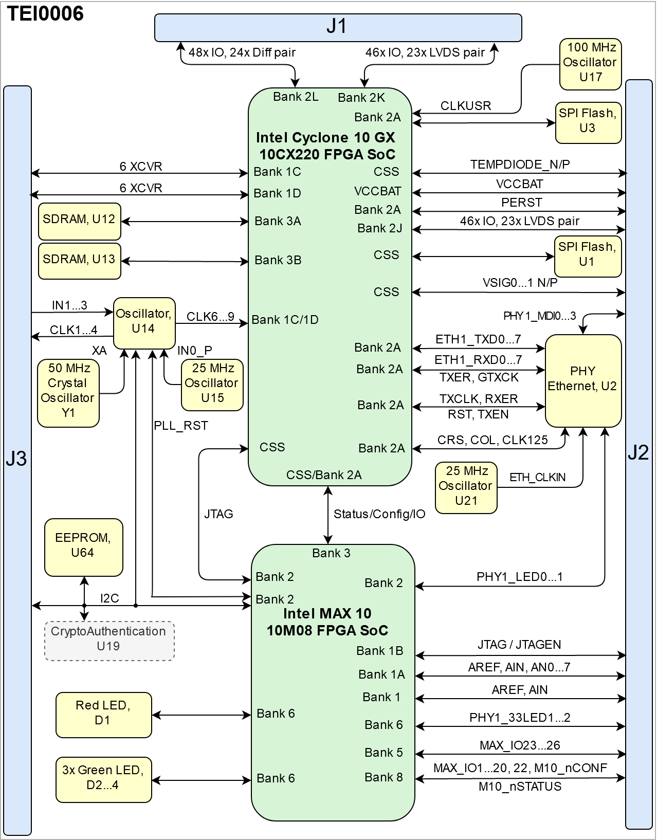
he The Trenz Electronic TEI0006 is an Industrial grade module based on Intel® Cyclone 10 GX. Intel Cyclone 10 GX device family delivers higher core, transceiver, and I/O performance than the previous generation of low cost FPGAs.
...
- Intel® Cyclone 10 GX Industrial [10CX220YF780I5G]
- Package: 780-FBGA
- Speed Grade: 5 (Fastest)
- Temperature: -40°C ~ 100°C
- Package compatible device 10CX150 and 10CX105 as assembly variant on request possible
- 2x SDRAM DDR3L Memory IC 8Gb, 800MHz
- 2x SPI Flash, 1 Gb
- 2x Transceiver Full Ethernet 64-QFN
- Programmable Oscillator
- 2Kb EEPROM Memory, 2Kb
4x User LED
- I/O interfaces:
Board to Board (B2B):
- Plug-on module with 3 x 160-pin Samtec Razor Beam (ST5) connectors
Power Supply:
Others:
...
| Scroll Title |
|---|
| anchor | Figure_OV_BD |
|---|
| title | TEI0006 block diagram |
|---|
|
| Scroll Ignore |
|---|
| draw.io Diagram |
|---|
| border | false |
|---|
| viewerToolbar | true |
|---|
| |
|---|
| fitWindow | false |
|---|
| diagramName | TEI0006_OV_BD |
|---|
| simpleViewer | false |
|---|
| links | auto |
|---|
| tbstyle | hidden |
|---|
| lbox | true |
|---|
| diagramWidth | 638 |
|---|
| revision | 1617 |
|---|
|
|
| Scroll Only |
|---|
|
|
Main Components
...
| Scroll Title |
|---|
| anchor | Table_OV_IDS |
|---|
| title | Initial delivery state of programmable devices on the module |
|---|
|
| Scroll Table Layout |
|---|
| orientation | portrait |
|---|
| sortDirection | ASC |
|---|
| repeatTableHeaders | default |
|---|
| sortByColumn | 1 |
|---|
| sortEnabled | false |
|---|
| cellHighlighting | true |
|---|
|
Storage device name | Content | Notes |
|---|
Quad SPI Flash | Not Programmed |
| | EEPROM | Programmed | Programmable Oscillator configuration | | DDR3 SDRAM | Not Programmed |
|
|
Configuration Signals
| Page properties |
|---|
|
- Overview of Boot Mode, Reset, Enables.
|
The TEI00006 TEI0006 module can be configured using different modes. Mode selection can be done using MSEL[2:0]. MSEL2 is potentially connected to GND so mode selection can be done using MSEL[1:0] which are connected to Bank 3 of Intel Max 10.
...
| Scroll Title |
|---|
| anchor | Table_SIP_B2B |
|---|
| title | General PL I/O to B2B connectors information |
|---|
|
| Scroll Table Layout |
|---|
| orientation | portrait |
|---|
| sortDirection | ASC |
|---|
| repeatTableHeaders | default |
|---|
| sortByColumn | 1 |
|---|
| sortEnabled | false |
|---|
| cellHighlighting | true |
|---|
|
| FPGA | FPGA Bank | B2B Connector | I/O Signal Count | Voltage Level | Notes |
|---|
| Intel Cyclone 10 GX | Bank 1C | J3 | 24 Single ended (12 Diff pair) | 0.95V | GXBL1C_RX0...5 N/P, GXBL1C_TX0...5 N/P | Bank 1D | J3 | 24 Single ended (12 Diff pair) | 0.95V | GXBL1D_RX0...5 N/P, GXBL1D_TX0...5 N/P | | Bank 2A | J2 |
1 | 2 Single ended | 1.8V | PERST, CLKUSR | | Bank 2J | J2 | 46 Single ended (23 Diff pair) | 1.8V |
| | Bank 2K | J1 | 46 Single ended (23 Diff pair) | VCCIO2K |
| | Bank 2L | J1 | 46 Single ended (23 Diff pair) | 3.0V |
| | Bank 3A | - | - | 1.35V | VDD_DDR | | Bank 3B | - | - | 1.35V | VDD_DDR | | Intel Max 10 | Bank 1A | J2 | 8 Single ended | 3.3V |
| | Bank 1B | J2 | 5 Single ended | 3.3V |
| | Bank 2 | J3 | 2 Single ended | 1.8VIO |
| | Bank 3 | - | - | 1.8VIO |
| | Bank 5 | J2 | 4 Single ended | 3.3V |
| | Bank 6 | J2 | 2 Single ended | 3.3V |
| | Bank 8 | J2 | 25 Single ended | 3.3V |
|
|
JTAG Interface
JTAG access to the TEI0006 SoM through B2B connector JM2.
| Scroll Title |
|---|
| anchor | Table_SIP_JTG |
|---|
| title | JTAG pins connection |
|---|
|
| Scroll Table Layout |
|---|
| orientation | portrait |
|---|
| sortDirection | ASC |
|---|
| repeatTableHeaders | default |
|---|
| sortByColumn | 1 |
|---|
| sortEnabled | false |
|---|
| cellHighlighting | true |
|---|
|
JTAG Signal | B2B Connector | Note |
|---|
| TMS | J2-160 |
| | TDI | J2-159 |
| | TDO | J2-158 |
| | TCK | J2-157 |
| | JTAG_ENJTAGEN | J2-105 | Connected to 3.3V |
|
MIO Pins
...
| Scroll Title |
|---|
| anchor | Table_OBP_EEP |
|---|
| title | I2C EEPROM interface MIOs and pins |
|---|
|
| Scroll Table Layout |
|---|
| orientation | portrait |
|---|
| sortDirection | ASC |
|---|
| repeatTableHeaders | default |
|---|
| sortByColumn | 1 |
|---|
| sortEnabled | false |
|---|
| cellHighlighting | true |
|---|
|
| Schematic | U64 Pin | B2B | Notes |
|---|
| I2C_SCL | SCL | J3-135 | Connected to Bank 2 of U18(Intel Max 10)- Bank 2 | | I2C_SDA | SDA | J3-137 | Connected to Bank 2 of to U18(Intel Max 10)- Bank 2 |
|
| Scroll Title |
|---|
| anchor | Table_OBP_I2C_EEPROM |
|---|
| title | I2C address for EEPROM |
|---|
|
| Scroll Table Layout |
|---|
| orientation | portrait |
|---|
| sortDirection | ASC |
|---|
| repeatTableHeaders | default |
|---|
| sortByColumn | 1 |
|---|
| sortEnabled | false |
|---|
| cellHighlighting | true |
|---|
|
| Pins | I2C Address | Designator | Notes |
|---|
| I2C_SCL, I2C_SDA | 0x53 | U64 |
|
|
...
| Scroll Title |
|---|
| anchor | Table_OBP_ETH |
|---|
| title | Ethernet PHY to Zynq Intel Cyclone 10 GX SoC connections |
|---|
|
| Scroll Table Layout |
|---|
| orientation | portrait |
|---|
| sortDirection | ASC |
|---|
| repeatTableHeaders | default |
|---|
| sortByColumn | 1 |
|---|
| sortEnabled | false |
|---|
| cellHighlighting | true |
|---|
|
| Signal Name | Connected to | B2B | Signal Description |
|---|
PHY1_MDI0_P PHY1_MDI0_N | - - | J2-93 J2-91 |
| PHY1_MDI1_P PHY1_MDI1_N | - - | J2-87 J2-85 |
| PHY1_MDI2_P PHY1_MDI2_N | - - | J2-81 J2-79 |
| PHY1_MDI3_P PHY1_MDI3_N | - - | J2-75 J2-73 |
| | ETH1_RST | Bank 2A | - | Connected to DVDDH Voltage | | ETH1_MDC | Bank 2A | - | Connected to DVDDH Voltage | | ETH1_MDIO | Bank 2A | - | Connected to DVDDH Voltage | | ETH1_TXD0...7 | Bank 2A | - | 8bit Transfer | | ETH1_RXD0...7 | Bank 2A | - | 8bit Recieve | | ETH1_GTXCK | Bank 2A | - |
| | ETH1_TXCLK | Bank 2A | - |
| | ETH1_TXEN | -Bank 2A | - |
| | ETH1_TXER | -Bank 2A | - |
| | ETH1_RXCK | Bank 2A | - | Connected to GNG | | ETH1_RXDV | Bank 2A | - | Connected to GNG | | PHY1_INT | - | - | Connected to DVDDH Voltage | | PHY1_LED1 | - | J2-69 | Connected to DVDDH Voltage | | PHY1_LED2 | - | J2-67 | Connected to GNG | | ETH1_CRS | Bank 2A | - |
| | ETH1_XTAL_IN | ETH_CLKIN | - | From U21 (25MHz MEMS Oschillator) |
|
...
The TEI0006 is equipped with an Intel MAX 10 device an Intel MAX 10 device which is a single-chip, non-volatile low-cost programmable logic device (PLD) to integrate the optimal set of system components. Intel MAX 10 (U18) is power and configuration controller on TEI0006 SoM.
| Scroll Title |
|---|
| anchor | Table_SIP_B2B |
|---|
| title | General PL I/O to B2B connectors information |
|---|
|
| Scroll Table Layout |
|---|
| orientation | portrait |
|---|
| sortDirection | ASC |
|---|
| repeatTableHeaders | default |
|---|
| sortByColumn | 1 |
|---|
| sortEnabled | false |
|---|
| cellHighlighting | true |
|---|
|
| Intel Max 10 Bank | Signals | Connected to | Description | Notes |
|---|
| Bank 1A | AIN0...7 | B2B- J2 |
|
| | Bank 1B | TCK, TDO, TMS, TDI, JTAGEN | B2B- J2 |
|
| | Bank 2 | PHY1_LED1 PHY1_LED2 | U23(Ethernet) U23(Ethernet) | Ethernet LED Ethernet LED | Tight to GND Tight to DVDDH | | F_TCK, F_TDO, F_TDI, F_TMS | U23(Intel Cyclone 10 GX) - Bank CSS | Intel Cyclone 10 JTAG signals |
| | I2C_SDA, I2C_SCL | U64(EEPROM) J3 (B2B) U14 (Programmable Oscillator) | I2C EEPROM signals |
| | PLL_RST | U14 (Programmable Oscillator) | Oscillator reset signal |
| | Bank 3 | nSTATUS, nCONFIG, CONF_DONE | U23(Intel Cyclone 10 GX) - Bank CSS | Intel Cyclone 10 Configuration signals |
| | DCLK | U23(Intel Cyclone 10 GX) - Bank CSS U1(SPI Flash) | Intel Cyclone 10 Configuration clock from Flash memory |
| | MSEL0...1 | U23(Intel Cyclone 10 GX) - Bank CSS | Intel Cyclone 10 Configuration mode signals |
| | DEV_CLRN, INIT_DONE | U23(Intel Cyclone 10 GX) - Bank 2A |
|
| | M10_IO0...4 | U23(Intel Cyclone 10 GX) - Bank 2A |
|
| Bank 5
| DIS_GROUP1...4 | T1...4 (N- Channel MOSFET) | Fast Discharching |
| | MAX_IO23...26 | J2 (B2B) | Intel MAX 10 GPIO |
| PG_0.95V, EN_0.95V PG_1.8VIO, EN_1.8VIO | U7(Voltage Regulator) U7(Voltage Regulator) | Power control signals |
| Bank 6
| M10_CLK | U21(25MHz Oscillator) | Intel MAX 10 Clock |
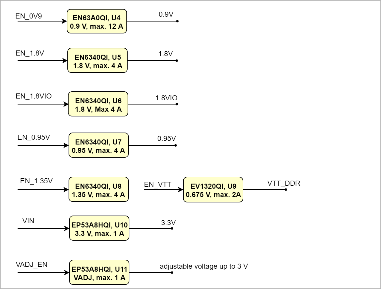
| VADJ_VS0...2, VADJ_EN PG_1.35V, EN_1.35V PG_1.8V, EN_1.8V PG_VTT, EN_VTT PG_0V9, EN_0V9 | U11(Voltage Regulator) U8(Voltage Regulator) U5(Voltage Regulator) U9(Voltage Regulator) U4(Voltage Regulator) | Power control signals |
| | PHY1_33LED1...2 | J2 (B2B) | Ethernet LED |
| LED_FP_1 LED_FP_2...4 | D1 D2...4 | User LEDs | Red LED Green LED | | Bank 8 | M10_nSTATUS, M10_nCONFIG, M10_CONF_DONE | J2(B2B) | Intel MAX 10 configuration signals |
| | MAX_IO1...22 | J2(B2B) | Intel MAX 10 GPIO |
|
|
...
| Scroll Title |
|---|
| anchor | Figure_PWR_PS |
|---|
| title | Power SequencySequence |
|---|
|
| Scroll Ignore |
|---|
| draw.io Diagram |
|---|
| border | false |
|---|
| viewerToolbar | true |
|---|
| |
|---|
| fitWindow | false |
|---|
| diagramDisplayName | |
|---|
| lbox | true |
|---|
| revision | 5 |
|---|
| diagramName | TEI0006_PWR_PS |
|---|
| simpleViewer | false |
|---|
| width | |
|---|
| links | auto |
|---|
| tbstyle | hidden |
|---|
| diagramWidth | 639 |
|---|
|
|
| Scroll Only |
|---|
|
|
...
| Scroll Title |
|---|
| anchor | Table_PWR_BV |
|---|
| title | SoC Bbank bank voltages. |
|---|
|
| Scroll Table Layout |
|---|
| orientation | portrait |
|---|
| sortDirection | ASC |
|---|
| repeatTableHeaders | default |
|---|
| sortByColumn | 1 |
|---|
| sortEnabled | false |
|---|
| cellHighlighting | true |
|---|
|
| FPGA | FPGA Bank | Voltage Level | Notes |
|---|
| Intel Cyclone 10 GX | Bank 1C | 0.95 V |
| Bank 1D | 0.95 V |
| | Bank 2A | 1.8 V |
| | Bank 2J | 1.8 V | VCCIO2J | | Bank 2K | 1.8 V | VCCIO2K | | Bank 2L | 3.0 V |
| | Bank 3A | 1.35 V | VDD_DDR | | Bank 3B | 1.35 V | VDD_DDR | | Intel Max 10 | Bank 1A | 3.3 V |
| | Bank 1B | 3.3 V |
| | Bank 2 | 1.8 V | 1.8VIO | | Bank 3 | 1.8 V | 1.8VIO | | Bank 5 | 3.3V |
| | Bank 6 | 3.3V |
| | Bank 8 | 3.3V |
|
|
...
| Scroll Title |
|---|
| anchor | Table_TS_AMR |
|---|
| title | Absolute maximum ratings |
|---|
|
| Scroll Table Layout |
|---|
| orientation | portrait |
|---|
| sortDirection | ASC |
|---|
| repeatTableHeaders | default |
|---|
| sortByColumn | 1 |
|---|
| sortEnabled | false |
|---|
| cellHighlighting | true |
|---|
|
| Symbols | Description | Min | Max | Unit | Note |
|---|
| VCC | Core voltage power supply | -0.5 | 1.21 | V |
| | VCCP | Periphery circuitry and transceiver fabric interface power supply | -0.5 | 1.21 | V |
| | VCCERAM | Embedded memory power supply | -0.5 | 1.36 | V |
| | VCCPT | Power supply for programmable power technology and I/O pre-driver | -0.5 | 2.46 | V |
| | VCCIO | I/O buffers power supply | -0.5 | 4.10 | V | 3 V I/O | -0.5 | 2.46 | LVDS I/O | | VCCA_PLL | Phase-locked loop (PLL) analog power supply | -0.5 | 2.46 | V |
| | VCCT_GXB | Transmitter power supply | -0.5 | 1.34 | V |
| | VCCR_GXB | Receiver power supply | -0.5 | 1.34 | V |
| | VCCH_GXB | Transceiver output buffer power supply | -0.5 | 2.46 | V |
| | T_STG | Storage temperature | -55 | 125 | °C |
|
|
...
Physical Dimensions
...
| Scroll Title |
|---|
| anchor | Table_VCP_SO |
|---|
| title | Trenz Electronic Shop Overview |
|---|
|
| Scroll Table Layout |
|---|
| orientation | portrait |
|---|
| sortDirection | ASC |
|---|
| repeatTableHeaders | default |
|---|
| sortByColumn | 1 |
|---|
| sortEnabled | false |
|---|
| cellHighlighting | true |
|---|
|
|
...
| Scroll Title |
|---|
| anchor | Table_RH_HRH |
|---|
| title | Hardware Revision History |
|---|
|
| Scroll Table Layout |
|---|
| orientation | portrait |
|---|
| sortDirection | ASC |
|---|
| repeatTableHeaders | default |
|---|
| sortByColumn | 1 |
|---|
| sortEnabled | false |
|---|
| cellHighlighting | true |
|---|
|
| Date | Revision | Changes | Documentation Link |
|---|
| 2018-07-27 | 01 | - | REV01 |
|
Document Change History
| Page properties |
|---|
|
- Note this list must be only updated, if the document is online on public doc!
- It's semi automatically, so do following
Add new row below first Copy "Page Information Macro(date)" Macro-Preview, Metadata Version number, Author Name and description to the empty row. Important Revision number must be the same as the Wiki document revision number Update Metadata = "Page Information Macro (current-version)" Preview+1 and add Author and change description. --> this point is will be deleted on newer pdf export template - Metadata is only used of compatibility of older exports
|
...