Download PDF version of this document.
Table of Contents
Overview
The Trenz Electronic TEI0006 is an Industrial grade module based on Intel® Cyclone 10 GX. Intel Cyclone 10 GX device family delivers higher core, transceiver, and I/O performance than the previous generation of low cost FPGAs.
Refer to http://trenz.org/tei0006-info for the current online version of this manual and other available documentation.
Key Features
- Intel® Cyclone 10 GX Industrial [10CX220YF780I5G]
- Package: 780-FBGA
- Speed Grade: 5 (Fastest)
- Temperature: -40°C ~ 100°C
- Package compatible device 10CX150 and 10CX105 as assembly variant on request possible
- 2x SDRAM DDR3L Memory IC 8Gb, 800MHz
- 2x SPI Flash, 1 Gb
- 2x Transceiver Full Ethernet 64-QFN
- Programmable Oscillator
- 2Kb EEPROM Memory
4x User LED
- I/O interfaces:
- 284 GPIO
- 118 LVDS
- 12 XCVR
Board to Board (B2B):
- Plug-on module with 3 x 160-pin Samtec Razor Beam (ST5) connectors
Power Supply:
5V
Others:
Dimension: 80m x 60m
Block Diagram
TEI0006 block diagram
Main Components
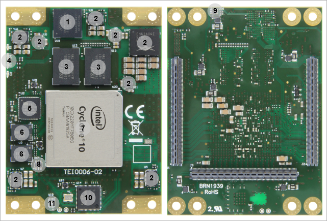
TEI0006 main components
- Intel® MAX 10, U18
- DC/DC convertor, U4...11
- SDRAM DDR3 Memory, U12...13
- User LEDs, D1...4
- Ethernet Tranciever, U2- U14
- SPI Flash Memory, U1- U3
- Intel® Cyclone 10 GX, U23
- EEPROM, U64
- Buffer, U16
Initial Delivery State
Storage device name | Content | Notes |
|---|---|---|
Quad SPI Flash | Not Programmed | |
| EEPROM | Programmed | Programmable Oscillator configuration |
| DDR3 SDRAM | Not Programmed |
Initial delivery state of programmable devices on the module
Configuration Signals
The TEI0006 module can be configured using different modes. Mode selection can be done using MSEL[2:0]. MSEL2 is potentially connected to GND so mode selection can be done using MSEL[1:0] which are connected to Bank 3 of Intel Max 10.
MODE Signal State | MSEL2 | MSEL1 | MSEL0 | Boot Mode |
|---|---|---|---|---|
MSEL[2:0] | 0 | 1 | 0 | AS x4 / Fast |
| 0 | 1 | 1 | AS x1 / Standard | |
| 0 | 0 | 0 | PS and FPP/ Fast | |
| 0 | 0 | 1 | PS and FPP/ Standard |
Boot process.
By tying the CONF_DONE, nSTATUS, and nCONFIG pins together, the devices initialize and enter user mode at the same time. If any device in the chain detects an error, configuration stops for the entire chain and you must reconfigure all the devices. For example, if the first device in the chain flags an error on the nSTATUS pin, it resets the chain by pulling its nSTATUS pin low.
| Signals | Connected to | Description | Note |
|---|---|---|---|
| nCONFIG | 1.8V | Configuration trigger | From U18( Intel MAX 10) - Bank 3 |
| CONF_DONE | 1.8V | Configuration done | To U18( Intel MAX 10) - Bank 3 |
| nSTATUS | 1.8V | Configuration status | To U18( Intel MAX 10) - Bank 3 |
| DCLK | U1,U3 | Configuration clock | To U1(Flash Memory) From U18( Intel MAX 10) - Bank 3 |
| AS_DATA0...3 | U1 | Configuration data | To U1(Flash Memory) |
Configuration signals.
Signal | B2B | Connected to | Note |
|---|---|---|---|
PERST | J2-99 | Bank A2 |
Reset process.
Signals, Interfaces and Pins
Board to Board (B2B) I/Os
FPGA bank number and number of I/O signals connected to the B2B connector:
| FPGA | FPGA Bank | B2B Connector | I/O Signal Count | Voltage Level | Notes |
|---|---|---|---|---|---|
| Intel Cyclone 10 GX | Bank 1C | J3 | 24 Single ended (12 Diff pair) | 0.95V | GXBL1C_RX0...5 N/P, GXBL1C_TX0...5 N/P |
Bank 1D | J3 | 24 Single ended (12 Diff pair) | 0.95V | GXBL1D_RX0...5 N/P, GXBL1D_TX0...5 N/P | |
| Bank 2A | J2 | 2 Single ended | 1.8V | PERST, CLKUSR | |
| Bank 2J | J2 | 46 Single ended (23 Diff pair) | 1.8V | ||
| Bank 2K | J1 | 46 Single ended (23 Diff pair) | VCCIO2K | ||
| Bank 2L | J1 | 46 Single ended (23 Diff pair) | 3.0V | ||
| Bank 3A | - | - | 1.35V | VDD_DDR | |
| Bank 3B | - | - | 1.35V | VDD_DDR | |
| Intel Max 10 | Bank 1A | J2 | 8 Single ended | 3.3V | |
| Bank 1B | J2 | 5 Single ended | 3.3V | ||
| Bank 2 | J3 | 2 Single ended | 1.8VIO | ||
| Bank 3 | - | - | 1.8VIO | ||
| Bank 5 | J2 | 4 Single ended | 3.3V | ||
| Bank 6 | J2 | 2 Single ended | 3.3V | ||
| Bank 8 | J2 | 25 Single ended | 3.3V |
General PL I/O to B2B connectors information
JTAG Interface
JTAG access to the TEI0006 SoM through B2B connector JM2.
JTAG Signal | B2B Connector | Note |
|---|---|---|
| TMS | J2-160 | |
| TDI | J2-159 | |
| TDO | J2-158 | |
| TCK | J2-157 | |
| JTAGEN | J2-105 | Connected to 3.3V |
JTAG pins connection
MIO Pins
| MIO Pin | Connected to | B2B | Notes |
|---|---|---|---|
| MAX_IO1...22 | U18( Intel MAX 10) - Bank 8 | J2 | |
| MAX_IO23...26 | U18( Intel MAX 10) - Bank 8 | J2 |
MIOs pins
On-board Peripherals
| Chip/Interface | Designator | Notes |
|---|---|---|
| U1- U3 | ||
| EEPROM | U64 | |
| SDRAM DDR3 Memory | U12...13 | |
| Ethernet Tranciever | U2- U14 | |
| Intel Max 10 | U18 | |
| D1...4 | D1 (Red), D2...4 (Green) | |
| Oscillators | U14, U15, U17, U21 |
On board peripherals
SPI Flash Memory
The TEI0006 is equipped with two Micron SPI flash memory. On-board SPI flash memory is used to store initial FPGA configuration. Besides FPGA configuration, remaining free flash memory can be used for user application and data storage. All four SPI data lines are connected to the FPGA allowing x1 or x4 data bus widths. Maximum data rate depends on the selected bus width and clock frequency.
| Designator | Schematic | Connected to | Notes |
|---|---|---|---|
| U1 | NCSO | CSS Bank (Configuration Bank) | Used when you are not configuring using AS |
| DCK | DCLK | AS Configuration Clock | |
| AS_DATA0 | CSS Bank (Configuration Bank) | AS Configuration Pin | |
| AS_DATA1 | CSS Bank (Configuration Bank) | AS Configuration Data | |
| AS_DATA2 | CSS Bank (Configuration Bank) | AS Configuration Data | |
| AS_DATA3 | CSS Bank (Configuration Bank) | AS Configuration Data | |
| U3 | QSPI_CS | Bank 2A | |
| QSPI_CK | Bank 2A | ||
| QSPI_DATA0 | Bank 2A | ||
| QSPI_DATA1 | Bank 2A | ||
| QSPI_DATA2 | Bank 2A | ||
| QSPI_DATA3 | Bank 2A |
Quad SPI interface MIOs and pins
EEPROM
| Schematic | U64 Pin | B2B | Notes |
|---|---|---|---|
| I2C_SCL | SCL | J3-135 | Connected to U18(Intel Max 10)- Bank 2 |
| I2C_SDA | SDA | J3-137 | Connected to U18(Intel Max 10)- Bank 2 |
I2C EEPROM interface MIOs and pins
| Pins | I2C Address | Designator | Notes |
|---|---|---|---|
| I2C_SCL, I2C_SDA | 0x53 | U64 |
I2C address for EEPROM
DDR3 SDRAM
The TEI0006 SoM has two 1 Gb volatile DDR3 SDRAM IC for storing user application code and data.
- Part number: IS43TR16512BL
- Supply voltage: 1.35V
- Speed: 800MHz
- Temperature: 0 ° C to 95 ° C
Ethernet
| Signal Name | Connected to | B2B | Signal Description |
|---|---|---|---|
PHY1_MDI0_P PHY1_MDI0_N | - - | J2-93 J2-91 | |
PHY1_MDI1_P PHY1_MDI1_N | - - | J2-87 J2-85 | |
PHY1_MDI2_P PHY1_MDI2_N | - - | J2-81 J2-79 | |
PHY1_MDI3_P PHY1_MDI3_N | - - | J2-75 J2-73 | |
| ETH1_RST | Bank 2A | - | Connected to DVDDH Voltage |
| ETH1_MDC | Bank 2A | - | Connected to DVDDH Voltage |
| ETH1_MDIO | Bank 2A | - | Connected to DVDDH Voltage |
| ETH1_TXD0...7 | Bank 2A | - | 8bit Transfer |
| ETH1_RXD0...7 | Bank 2A | - | 8bit Recieve |
| ETH1_GTXCK | Bank 2A | - | |
| ETH1_TXCLK | Bank 2A | - | |
| ETH1_TXEN | Bank 2A | - | |
| ETH1_TXER | Bank 2A | - | |
| ETH1_RXCK | Bank 2A | - | Connected to GNG |
| ETH1_RXDV | Bank 2A | - | Connected to GNG |
| PHY1_INT | - | - | Connected to DVDDH Voltage |
| PHY1_LED1 | - | J2-69 | Connected to DVDDH Voltage |
| PHY1_LED2 | - | J2-67 | Connected to GNG |
| ETH1_CRS | Bank 2A | - | |
| ETH1_XTAL_IN | ETH_CLKIN | - | From U21 (25MHz MEMS Oschillator) |
Ethernet PHY to Intel Cyclone 10 GX SoC connections
Intel MAX 10
The TEI0006 is equipped with an Intel MAX 10 device which is a single-chip, non-volatile low-cost programmable logic device (PLD) to integrate the optimal set of system components. Intel MAX 10 (U18) is power and configuration controller on TEI0006 SoM.
| Intel Max 10 Bank | Signals | Connected to | Description | Notes |
|---|---|---|---|---|
| Bank 1A | AIN0...7 | B2B- J2 | ||
| Bank 1B | TCK, TDO, TMS, TDI, JTAGEN | B2B- J2 | ||
| Bank 2 | PHY1_LED1 PHY1_LED2 | U23(Ethernet) U23(Ethernet) | Ethernet LED Ethernet LED | Tight to GND Tight to DVDDH |
| F_TCK, F_TDO, F_TDI, F_TMS | U23(Intel Cyclone 10 GX) - Bank CSS | Intel Cyclone 10 JTAG signals | ||
| I2C_SDA, I2C_SCL | U64(EEPROM) J3 (B2B) U14 (Programmable Oscillator) | I2C EEPROM signals | ||
| PLL_RST | U14 (Programmable Oscillator) | Oscillator reset signal | ||
| Bank 3 | nSTATUS, nCONFIG, CONF_DONE | U23(Intel Cyclone 10 GX) - Bank CSS | Intel Cyclone 10 Configuration signals | |
| DCLK | U23(Intel Cyclone 10 GX) - Bank CSS U1(SPI Flash) | Intel Cyclone 10 Configuration clock from Flash memory | ||
| MSEL0...1 | U23(Intel Cyclone 10 GX) - Bank CSS | Intel Cyclone 10 Configuration mode signals | ||
| DEV_CLRN, INIT_DONE | U23(Intel Cyclone 10 GX) - Bank 2A | |||
| M10_IO0...4 | U23(Intel Cyclone 10 GX) - Bank 2A | |||
| Bank 5 | DIS_GROUP1...4 | T1...4 (N- Channel MOSFET) | Fast Discharching | |
| MAX_IO23...26 | J2 (B2B) | Intel MAX 10 GPIO | ||
PG_0.95V, EN_0.95V PG_1.8VIO, EN_1.8VIO | U7(Voltage Regulator) U7(Voltage Regulator) | Power control signals | ||
| Bank 6 | M10_CLK | U21(25MHz Oscillator) | Intel MAX 10 Clock | |
VADJ_VS0...2, VADJ_EN PG_1.35V, EN_1.35V PG_1.8V, EN_1.8V PG_VTT, EN_VTT PG_0V9, EN_0V9 | U11(Voltage Regulator) U8(Voltage Regulator) U5(Voltage Regulator) U9(Voltage Regulator) U4(Voltage Regulator) | Power control signals | ||
| PHY1_33LED1...2 | J2 (B2B) | Ethernet LED | ||
LED_FP_1 LED_FP_2...4 | D1 D2...4 | User LEDs | Red LED Green LED | |
| Bank 8 | M10_nSTATUS, M10_nCONFIG, M10_CONF_DONE | J2(B2B) | Intel MAX 10 configuration signals | |
| MAX_IO1...22 | J2(B2B) | Intel MAX 10 GPIO |
General PL I/O to B2B connectors information
LEDs
| Designator | Color | Connected to | Active Level | Note |
|---|---|---|---|---|
| D1 | Red | LED_FP_1 | Active high | |
| D2 | Green | LED_FP_2 | Active high | |
| D3 | Green | LED_FP_3 | Active high | |
| D4 | Green | LED_FP_4 | Active high |
On-board LEDs
Clock Sources
The TEI0006 has three MEMS oscillator and a programmable clock generator.
| Designator | Description | Frequency | Note |
|---|---|---|---|
| U21 | MEMS Oscillator | 25MHz | |
| U15 | MEMS Oscillator | 25MHz | |
| U17 | MEMS Oscillator | 48MHz | |
| U14 | Programmable Oscillator | Variable |
Osillators
| Signals | Clock Type | In/ Out | Connected to | Frequency | Note |
|---|---|---|---|---|---|
IN1_P IN1_N | Differential | In In | U15 (Oscillator) GND | 25 MHz | |
| IN1..3 | Differential | In | J3(B2B) | Variable | |
XA XB | Differential | U17 (Oscillator) GND | 48 MHz | ||
CLK0...4 | Differential | Out | J3(B2B) | 25MHz | |
| REFCLK_EMIFP | Differential | Out | - | Variable | |
| CLK6...7 | Differential | Out | U23 (Intel Cyclon 10 GX)- Bank 1D | Variable | |
| CLK8...9 | Differential | Out | U23 (Intel Cyclon 10 GX)- Bank 1C | Variable |
Programmable Oscillator connections
Power and Power-On Sequence
Power Supply
Power supply with minimum current capability of 2.5 A for system startup is recommended.
Power Consumption
| Power Input Pin | Typical Current |
|---|---|
| VIN | TBD* |
Power Consumption
* TBD - To Be Determined
Power Distribution Dependencies
Power Distribution
Power-On Sequence
Voltage regulators can be enabled through U18(Intel MAX 10)- Bank 6.
Power Sequence
Power Rails
| Power Rail Name | B2B Connector JM1 Pin | B2B Connector JM2 Pin | B2B Connector JM3 Pin | Voltage Level | Direction | Notes |
|---|---|---|---|---|---|---|
| VCCIO2K | 53, 54 | - | - | 1.8 V | Input | |
| VADJ | 140,142 | - | - | 3.0 V | Output | |
| VCCIO2J | - | 29,30 | 1.8 V | Input | ||
3.3V | - | 149,150 | - | 3.3 V | Output | |
| 1.8_VIO | - | - | 139 | 1.8 V | Output |
Module power rails.
Bank Voltages
| FPGA | FPGA Bank | Voltage Level | Notes |
|---|---|---|---|
| Intel Cyclone 10 GX | Bank 1C | 0.95 V | |
Bank 1D | 0.95 V | ||
| Bank 2A | 1.8 V | ||
| Bank 2J | 1.8 V | VCCIO2J | |
| Bank 2K | 1.8 V | VCCIO2K | |
| Bank 2L | 3.0 V | ||
| Bank 3A | 1.35 V | VDD_DDR | |
| Bank 3B | 1.35 V | VDD_DDR | |
| Intel Max 10 | Bank 1A | 3.3 V | |
| Bank 1B | 3.3 V | ||
| Bank 2 | 1.8 V | 1.8VIO | |
| Bank 3 | 1.8 V | 1.8VIO | |
| Bank 5 | 3.3V | ||
| Bank 6 | 3.3V | ||
| Bank 8 | 3.3V |
SoC bank voltages.
Board to Board Connectors
TEI0006 module has three Samtec Razor Beam LP Terminal Strip (ST5) on the bottom side.
- 3x REF-192552-02 (160-pins, 80 pins per row)
- ST5 Mates with SS5
Operating Temperature: -55°C ~ 125°C
Current Rating: 1.6 A per ContactNumber of Positions: ??
The module has a 160-pin double-row REF-192552-02 connector on the bottom side. The counterpart REF-192552-01 is placed on the base board.
Order | REF Number | Samtec Number | Type | Mated Height | Data sheet | Comment |
|---|---|---|---|---|---|---|
| 27220 | REF-192552-02 | ST5-80-1.50-L-D-P-TR | Module connector | 5 mm | http://suddendocs.samtec.com/catalog_english/st5.pdf | Standard connector used on module |
| 27219 | REF-192552-01 | SS5-80-3.50-L-D-K-TR | Baseboard connector | 5 mm | http://suddendocs.samtec.com/catalog_english/ss5.pdf | Standard connector used on board |
Connectors.
With different connectors from the used series other mating heights are possible (according to the Datasheet). The module and base board can be manufactured using other connectors upon request.
| Connector Specifications | Value |
|---|---|
| Insulator material | Liquid crystal polymer |
| Stacking height | 5 mm |
| Contact material | Phosphor-bronze |
| Plating | Au or Sn over 50 μ" (1.27 μm) Ni |
| Current rating | 1.6 A per pin (2 pins powered) |
| Operating temperature range | -55 °C to +125 °C |
| RoHS compliant | Yes |
Connector specifications.
Connector Speed Ratings
The LSHM connector speed rating depends on the stacking height; please see the following table:
| Stacking height | Speed rating |
|---|---|
| 5 mm, Single-Ended | 13.5GHz / 27Gbps |
| 5 mm, Differential | 20GHz / 40Gbps |
| 4 mm, Single-Ended | 13GHz / 26Gbps |
| 4 mm, Differential | 13.5GHz / 27Gbps |
Speed rating.
Current Rating
Current rating of Samtec Razor Beam™ SS5/ST5 B2B connectors is 1.6A per pin (2 pins powered).
Connector Mechanical Ratings
- Shock: 100G, 6 ms sawtooth wave
- Vibration: 7.56G 'RMS', 2 hours per axis, 3 axes total
Manufacturer Documentation
Technical Specifications
Absolute Maximum Ratings
| Symbols | Description | Min | Max | Unit | Note |
|---|---|---|---|---|---|
| VCC | Core voltage power supply | -0.5 | 1.21 | V | |
| VCCP | Periphery circuitry and transceiver fabric interface power supply | -0.5 | 1.21 | V | |
| VCCERAM | Embedded memory power supply | -0.5 | 1.36 | V | |
| VCCPT | Power supply for programmable power technology and I/O pre-driver | -0.5 | 2.46 | V | |
| VCCIO | I/O buffers power supply | -0.5 | 4.10 | V | 3 V I/O |
| VCCA_PLL | Phase-locked loop (PLL) analog power supply | -0.5 | 2.46 | V | |
| VCCT_GXB | Transmitter power supply | -0.5 | 1.34 | V | |
| VCCR_GXB | Receiver power supply | -0.5 | 1.34 | V | |
| VCCH_GXB | Transceiver output buffer power supply | -0.5 | 2.46 | V | |
| T_STG | Storage temperature | -55 | 125 | °C |
Absolute maximum ratings
Recommended Operating Conditions
Operating temperature range depends also on customer design and cooling solution. Please contact us for options.
| Parameter | Min | Max | Units | Reference Document |
|---|---|---|---|---|
| VCC | 0.87 | 0.93 | V | See Intel Cyclone 10 GX datasheet. |
| VCCP | 0.87 | 0.93 | V | See Intel Cyclone 10 GX datasheet. |
| VCCERAM | 0.87 | 0.93 | V | See Intel Cyclone 10 GX datasheet. |
| VCCPT | 1.71 | 1.89 | V | See Intel Cyclone 10 GX datasheet. |
| VCCPGM | 1.71 | 1.89 | V | See Intel Cyclone 10 GX datasheet. |
| VCCIO | 2.85 | 3.15 | V | See Intel Cyclone 10 GX datasheet. |
| VCCA_PLL | 1.71 | 1.89 | V | See Intel Cyclone 10 GX datasheet. |
| T_J | 0 | 85 | °C | See Intel Cyclone 10 GX datasheet. |
Recommended operating conditions.
Physical Dimensions
Module size: 60 mm × 80 mm. Please download the assembly diagram for exact numbers.
Mating height with standard connectors: 5 mm.
- PCB thickness: 1.65 mm
Physical Dimension
Currently Offered Variants
| Trenz shop TEI0006 overview page | |
|---|---|
| English page | German page |
Trenz Electronic Shop Overview
Revision History
Hardware Revision History
| Date | Revision | Changes | Documentation Link |
|---|---|---|---|
| 2018-07-27 | 01 | - | REV01 |
Hardware Revision History
Document Change History
| Date | Revision | Contributor | Description |
|---|---|---|---|
| |||
-- | all |
|
Document change history.
Disclaimer
Data Privacy
Please also note our data protection declaration at https://www.trenz-electronic.de/en/Data-protection-Privacy
Document Warranty
The material contained in this document is provided “as is” and is subject to being changed at any time without notice. Trenz Electronic does not warrant the accuracy and completeness of the materials in this document. Further, to the maximum extent permitted by applicable law, Trenz Electronic disclaims all warranties, either express or implied, with regard to this document and any information contained herein, including but not limited to the implied warranties of merchantability, fitness for a particular purpose or non infringement of intellectual property. Trenz Electronic shall not be liable for errors or for incidental or consequential damages in connection with the furnishing, use, or performance of this document or of any information contained herein.
Limitation of Liability
In no event will Trenz Electronic, its suppliers, or other third parties mentioned in this document be liable for any damages whatsoever (including, without limitation, those resulting from lost profits, lost data or business interruption) arising out of the use, inability to use, or the results of use of this document, any documents linked to this document, or the materials or information contained at any or all such documents. If your use of the materials or information from this document results in the need for servicing, repair or correction of equipment or data, you assume all costs thereof.
Copyright Notice
No part of this manual may be reproduced in any form or by any means (including electronic storage and retrieval or translation into a foreign language) without prior agreement and written consent from Trenz Electronic.
Technology Licenses
The hardware / firmware / software described in this document are furnished under a license and may be used /modified / copied only in accordance with the terms of such license.
Environmental Protection
To confront directly with the responsibility toward the environment, the global community and eventually also oneself. Such a resolution should be integral part not only of everybody's life. Also enterprises shall be conscious of their social responsibility and contribute to the preservation of our common living space. That is why Trenz Electronic invests in the protection of our Environment.
REACH, RoHS and WEEE
REACH
Trenz Electronic is a manufacturer and a distributor of electronic products. It is therefore a so called downstream user in the sense of REACH. The products we supply to you are solely non-chemical products (goods). Moreover and under normal and reasonably foreseeable circumstances of application, the goods supplied to you shall not release any substance. For that, Trenz Electronic is obliged to neither register nor to provide safety data sheet. According to present knowledge and to best of our knowledge, no SVHC (Substances of Very High Concern) on the Candidate List are contained in our products. Furthermore, we will immediately and unsolicited inform our customers in compliance with REACH - Article 33 if any substance present in our goods (above a concentration of 0,1 % weight by weight) will be classified as SVHC by the European Chemicals Agency (ECHA).
RoHS
Trenz Electronic GmbH herewith declares that all its products are developed, manufactured and distributed RoHS compliant.
WEEE
Information for users within the European Union in accordance with Directive 2002/96/EC of the European Parliament and of the Council of 27 January 2003 on waste electrical and electronic equipment (WEEE).
Users of electrical and electronic equipment in private households are required not to dispose of waste electrical and electronic equipment as unsorted municipal waste and to collect such waste electrical and electronic equipment separately. By the 13 August 2005, Member States shall have ensured that systems are set up allowing final holders and distributors to return waste electrical and electronic equipment at least free of charge. Member States shall ensure the availability and accessibility of the necessary collection facilities. Separate collection is the precondition to ensure specific treatment and recycling of waste electrical and electronic equipment and is necessary to achieve the chosen level of protection of human health and the environment in the European Union. Consumers have to actively contribute to the success of such collection and the return of waste electrical and electronic equipment. Presence of hazardous substances in electrical and electronic equipment results in potential effects on the environment and human health. The symbol consisting of the crossed-out wheeled bin indicates separate collection for waste electrical and electronic equipment.
Trenz Electronic is registered under WEEE-Reg.-Nr. DE97922676.
Overview
Content Tools