Page History
...
- Create a Plattform Designer file: File → New
- Select "Qsys System File" and press "OK"
- A new window should open.
- Look for "hps" inside the search field, as visible in the following figure.
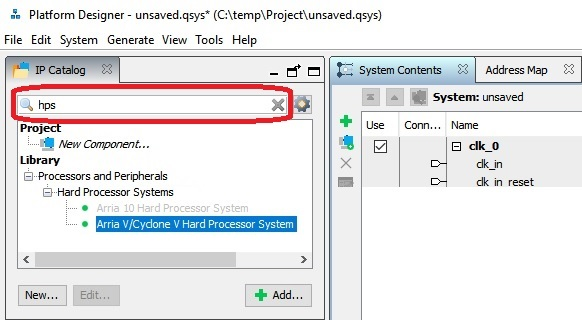
- Select "Arria V/Cyclone V Hard Processor System" via double click from the tree: Library → Processors and Peripherals → Hard Processor Systems → Arria V/Cyclone V Hard Processor System
- The window "Arria V/Cyclone V Hard Processor System - hps_0" should be opened as visible in the next figure.
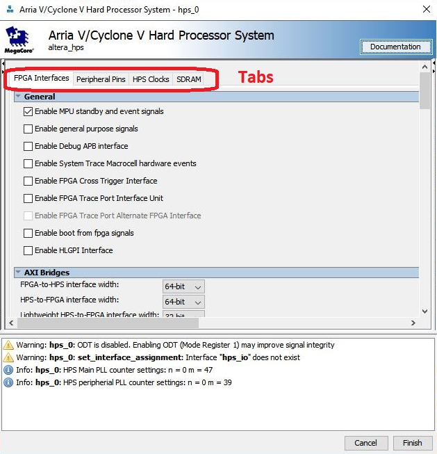
- In this window the HPS has to be configured with the following settings:
- Tab FPGA Interface:
- Uncheck "Enable MPU standby and event signals" (default)
AXI Bridges:
FPGA-to-HPS interface width: Unused
HPS-to-FPGA interface width: Unused
Lightweight HPS-to-FPGA interface width: Unused
- Tab Peripheral Pins:
- Quad SPI Flash Controller
- → QSPI pin: HPS I/O Set 0
- SD/MMC Controller
- → SDIO pin: HPS I/O Set 0
- → SDIO mode: 4-bit Data
- UART Controllers
- → UART0 pin: HPS I/O Set 0
- → UART0 mode: no Flow Control
- I2C Controllers
- → I2C0 pin: HPS I/O Set 1
- → I2C1 pin: HPS I/O Set 0
- Quad SPI Flash Controller
- Tab HPS Clocks:
- As is / Accept the default values (for both subtabs)
- Tab SDRAM
- Subtab Phy Settings:
- Memory clock frequency: 333.3 MHz
- PLL reference clock frequency: 25 MHz
Subtab - Memory Parameters:
Memory device speed grade: 800.0 MHz
Total interface width: 32 → 16 ???
Row Address width: 16
Column Address width: 10
- Memory Initialization Options
Memory CAS latency setting: 5
ODT Rtt nominal value: RZQ/6
Memory write CAS latency settings: 5
- Subtab Phy Settings:
- Subtab - Memory Timing:
- tIS (base): 180 ps
- tIH (base): 140 ps
- tDS (base): 30 ps
- tDH (base): 65 ps
- tDQSQ: 100 ps
- tQH: 0.38 cycles
- tDQSCK: 225 ps
- tDQSS: 0.27 cycles
- tQSH: 0.4 cycles
- tDSH: 0.18 cycles
- tDSS: 0.18 cycles
- tINIT: 500 us
- tMRD (tMRW): 4 cycles
- tRAS: 35.0 ns
- tRCD: 13.75 ns
- tRP: 13.75 ns
- tREFI (tREFIab): 7.8 us
- tRFC (tRFCab): 350.0 ns
- tWR: 15.0 ns
- tWTR: 4 cycles
- tFAW: 40 ns
- tRRD: 12.0 ns
- tRTP: 12.0 n
Subtab - Board Settings:
Board Skews
Maximum CK delay to DIMM/device: 0.03
Maximum DQS delay to DIMM/device: 0.02
Minimum delay difference between CK and DQS: 0.09
Maximum delay difference between CK and DQS: 0.16
Maximum skew within DQS group: 0.01
Maximum skew between DQS groups: 0.08
Maximum skew within address and command bus: 0.03
- Tab FPGA Interface:
- Click "Finish" to close the window "Arria V/Cyclone V Hard Processor System - hps_0".
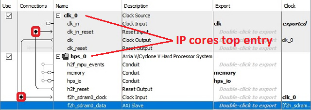
Add connections via clicking into the circle marked with a red rectangle in th next figure:
hps_0 - h2f_reset → clk_0 - clk_in_reset
clk_0 - clk → hps_0 - f2h_sdram0_data
- The HPS is nearly configured. Apply some auto functions:
System → Assign Base Addresses
System → Assign Interrupt Numbers
System → Assign Custom Instruction Opcodes
System → Create Global Reset Network
- Click Generate HDL... to generate the hardware description language file.
- Window "Generation" opens.
- In this window, under "Synthesis", select via dropdown menu in which Hardware Language your HDL will be created, Verilog or VHDL,
- Uncheck Create timing and resource estimate... .
- Check Create block symbole file (.bsf).
- Click Generate, as visible in the next figure.
...
Overview
Content Tools