This step guides through the tasks which have to be done inside Intel Quartus Prime. As mentionend in page "Board bring-up overview for TEI0022", this step is for project generation, system setting and output creation. Therefore, the work within this step should be explained in three sections:
- Project Creation
- System Setting
- Output Creation
The section "Project Creation" describes the basic work to create a new project. The second section "System Setting" explains the creation of an HPS instance inside the project. And the third section "Output Creation" shows how to create the result output inside Intel Quartus Prime.
Project Creation
This section guides through the project creation:
- Start Intel Quartus Prime
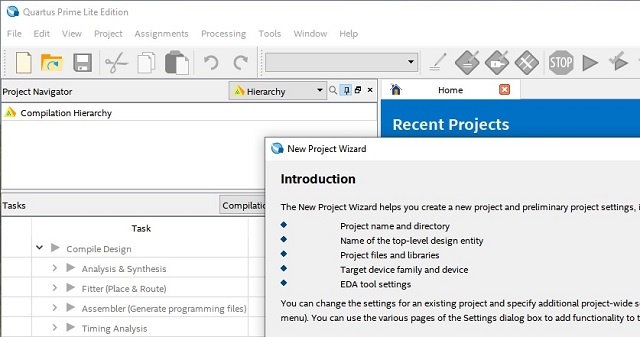
- Select: File → New Project Wizard...
Now, the following figure should be visible:
- Click Next >
- Select the project folder and the project name (e.g. HPSexample). Then, click Next >
- Select an "Empty project" and click Next > in the window "Project Type"
- Click Next > in the window "Add Files"
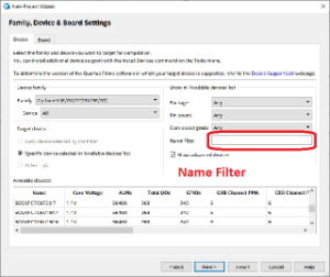
- Select the used FPGA in the window "Family, Device & Board Settings". For the board TEI0022, copy "5CSEMA5F31C8(N)" into the field "Name filter", select the "5CSEMA5F31C8(N)" SoC and click Next >.
- Click Next > in the window "EDA Tool Settings"
- Click Finish in the window "Summary"
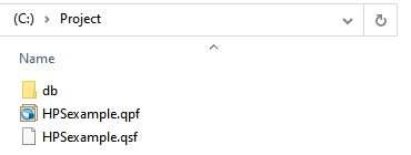
- The Intel Quartus project is generated and the folder should look like the next figure.
System Setting
This section guides through the system setting with the Plattform Designer to generate and configure the HPS according to the physical board resources.
- Create a Plattform Designer file: File → New
- Select "Qsys System File" and press "OK"
- A new window should open.
- Look for "hps" inside the search field, as visible in the following figure.
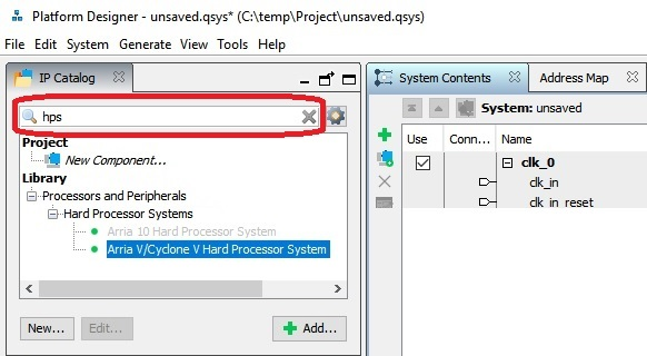
- Select "Arria V/Cyclone V Hard Processor System" via double click from the tree: Library → Processors and Peripherals → Hard Processor Systems → Arria V/Cyclone V Hard Processor System
- The window "Arria V/Cyclone V Hard Processor System - hps_0" should be opened as visible in the next figure.
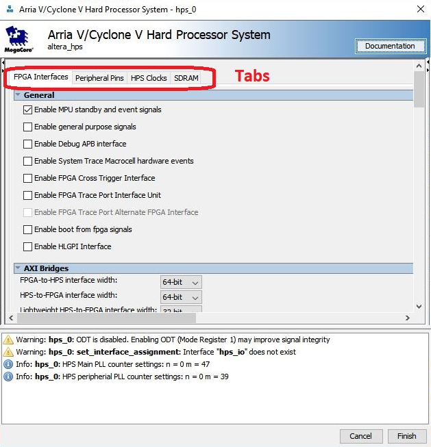
- In this window the HPS has to be configured with the following settings:
- Tab FPGA Interface:
- Uncheck "Enable MPU standby and event signals" (default)
AXI Bridges:
FPGA-to-HPS interface width: Unused
HPS-to-FPGA interface width: Unused
Lightweight HPS-to-FPGA interface width: Unused
- Tab Peripheral Pins:
- Quad SPI Flash Controller
- → QSPI pin: HPS I/O Set 0
- SD/MMC Controller
- → SDIO pin: HPS I/O Set 0
- → SDIO mode: 4-bit Data
- UART Controllers
- → UART0 pin: HPS I/O Set 0
- → UART0 mode: no Flow Control
- I2C Controllers
- → I2C0 pin: HPS I/O Set 1
- → I2C1 pin: HPS I/O Set 0
- Quad SPI Flash Controller
- Tab HPS Clocks:
- As is / Accept the default values (for both subtabs)
- Tab SDRAM
- Subtab Phy Settings:
- Memory clock frequency: 333.3 MHz
- PLL reference clock frequency: 25 MHz
Subtab - Memory Parameters:
Memory device speed grade: 800.0 MHz
Total interface width: 32
Row Address width: 16
Column Address width: 10
- Memory Initialization Options
Memory CAS latency setting: 5
ODT Rtt nominal value: RZQ/6
Memory write CAS latency settings: 5
- Subtab Phy Settings:
- Subtab - Memory Timing:
- tIS (base): 180 ps
- tIH (base): 140 ps
- tDS (base): 30 ps
- tDH (base): 65 ps
- tDQSQ: 100 ps
- tQH: 0.38 cycles
- tDQSCK: 225 ps
- tDQSS: 0.27 cycles
- tQSH: 0.4 cycles
- tDSH: 0.18 cycles
- tDSS: 0.18 cycles
- tINIT: 500 us
- tMRD (tMRW): 4 cycles
- tRAS: 35.0 ns
- tRCD: 13.75 ns
- tRP: 13.75 ns
- tREFI (tREFIab): 7.8 us
- tRFC (tRFCab): 350.0 ns
- tWR: 15.0 ns
- tWTR: 4 cycles
- tFAW: 40 ns
- tRRD: 12.0 ns
- tRTP: 12.0 n
Subtab - Board Settings:
Board Skews
Maximum CK delay to DIMM/device: 0.03
Maximum DQS delay to DIMM/device: 0.02
Minimum delay difference between CK and DQS: 0.09
Maximum delay difference between CK and DQS: 0.16
Maximum skew within DQS group: 0.01
Maximum skew between DQS groups: 0.08
Maximum skew within address and command bus: 0.03
- Tab FPGA Interface:
- Click "Finish" to close the window "Arria V/Cyclone V Hard Processor System - hps_0".
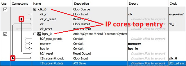
Add connections via clicking into the circle marked with a red rectangle in the next figure:
hps_0 - h2f_reset → clk_0 - clk_in_reset
clk_0 - clk → hps_0 - f2h_sdram0_data
- The HPS is nearly configured. Apply some auto functions:
System → Assign Base Addresses
System → Assign Interrupt Numbers
System → Assign Custom Instruction Opcodes
System → Create Global Reset Network
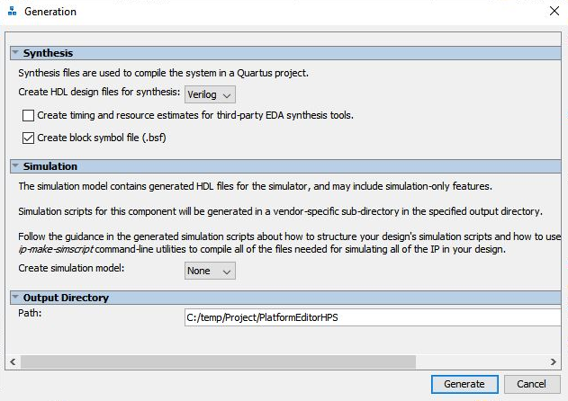
- Click Generate HDL... to generate the hardware description language file.
- Window "Generation" opens.
- In this window, under "Synthesis", select via dropdown menu in which Hardware Language your HDL will be created, Verilog or VHDL,
- Uncheck Create timing and resource estimate... .
- Check Create block symbole file (.bsf).
- Click Generate, as visible in the next figure.
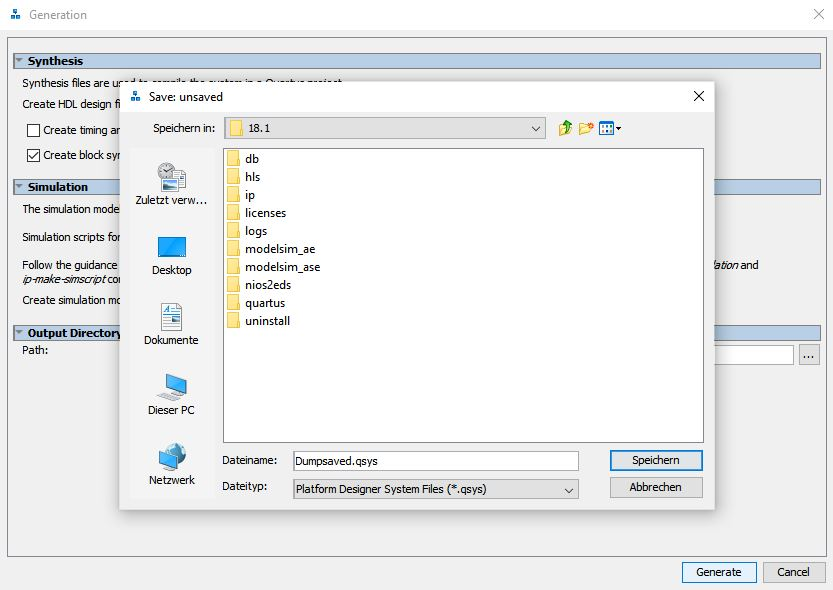
- Save the changes according to the opened saving dialogue, which is shown in the next figure.
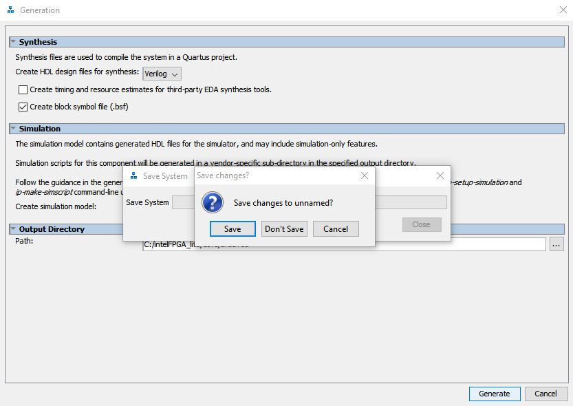
- Name the file (e.g. PlatformEditorHPS.qsys) and press Save, as visible in the next figure.
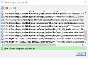
- After saving, the message "Save System: Completed successfully." should be shown and the view should be similar to the next figure.
- Press Close.
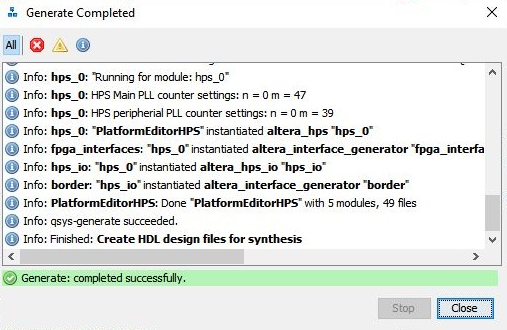
- Wait until the generation is finished and the message "Generation: Completed successfully." is shown according to the next figure.
- Press Close.
- Leave the Plattform Designer by pressing Finish.
- A notification appears, reminding to add files into the project, press OK.
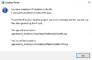
Close the Plattform Designer by pressing Finish.
Output Creation
This section guides through the output creation:
- Add the file "PlatformEditorHPS.qsys" to the project by using Project → Add/Remove Files in Project ...
Click onto the button with three dots (inside the red rectangle) in the opened window as visible in the next figure.
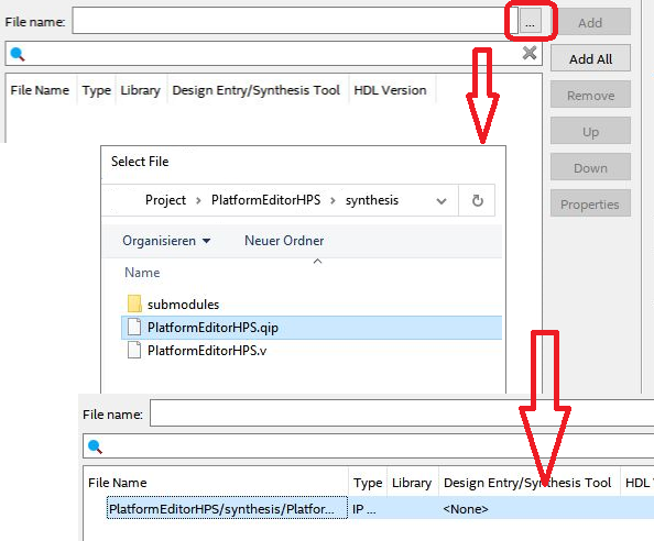
- In the "Select File" window select the file ... > PlatformEditorHPS → synthesis → PlatformEditorHPS.qip.
- Click OK.
- Change the view from "Hierarchy" to "Files" inside the drop-down menu withing the "Project Navigator".
- Set file "PlatformEditorHPS.qip" as top-level entity by right clicking onto the file and selecting Set as Top-Level Entity.
- Select Tools → Tcl Scripts...
- Select Project → PlatformEditorHPS → synthesis → submodules → hps_sdram_p0_pin_assignments.tcl and click Run.
- Confirm the notification and close the previous window through Close.
- Press Processing → Start Compilation
- Compilation process has to be finished without errors. Fix errors if there are some.
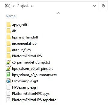
- The project folder should look like the following figure.
After this doing this guide, following files and folders are generated with the given purpose which are relevant for the next guide.
| File/Folder | Purpose |
|---|---|
| .sopcinfo | SOPC Info File containing hardware description for the Device Tree Generator |
| hps_isw_handoff | Folder containing a hardware description for the Preloader Generator |
Overview
Content Tools