...
| Scroll Title |
|---|
| anchor | Figure_OV_BD |
|---|
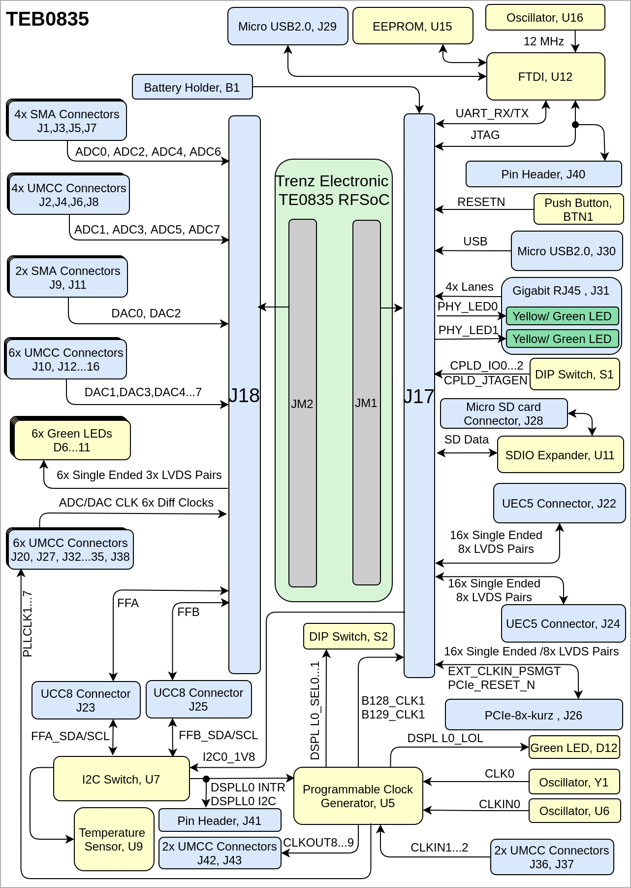
| title | TEB0835 block diagram |
|---|
|
| Scroll Ignore |
|---|
| draw.io Diagram |
|---|
| border | false |
|---|
| viewerToolbar | true |
|---|
| |
|---|
| fitWindow | false |
|---|
| diagramDisplayName | |
|---|
| lbox | true |
|---|
| revision | 15 |
|---|
| diagramName | TEB0835_OV_BD |
|---|
| simpleViewer | false |
|---|
| width | |
|---|
| links | auto |
|---|
| tbstyle | hidden |
|---|
| diagramWidth | 641 |
|---|
|
|
| Scroll Only |
|---|
|
|
...
| Scroll Title |
|---|
| anchor | Table_OV_BP |
|---|
| title | Boot process. |
|---|
|
| Scroll Table Layout |
|---|
| orientation | portrait |
|---|
| sortDirection | ASC |
|---|
| repeatTableHeaders | default |
|---|
| style | |
|---|
| widths | |
|---|
| sortByColumn | 1 |
|---|
| sortEnabled | false |
|---|
| cellHighlighting | true |
|---|
|
MODE Signal State | |Boot Mode |
|---|
|
| Scroll Title |
|---|
| anchor | Table_OV_RST |
|---|
| title | Reset process. |
|---|
|
| Scroll Table Layout |
|---|
| orientation | portrait |
|---|
| sortDirection | ASC |
|---|
| repeatTableHeaders | default |
|---|
style | widths | | sortByColumn | 1 |
|---|
| sortEnabled | false |
|---|
| cellHighlighting | true |
|---|
Signal | B2B | I/O | Note |
|---|
RESETN | J17- 36 | Input | Connected to Push Button, BTN1 |
Signals, Interfaces and Pins
| Page properties |
|---|
|
Notes : - For carrier or stand-alone boards use subsection for every connector type (add designator on description, not on the subsection title), for example:
- For modules which needs carrier use only classes and refer to B2B connector if more than one is used, for example
|
Board to Board (B2B) I/Os
FPGA bank number and number of I/O signals connected to the B2B connector:
MODE[0:3] | Boot Mode | Pin Location | Note |
|---|
0000 | PS_JTAG | JTAG | PSJTAG Interface | | 0001 | Quad SPI (24b) | MIO0...12 | QSPI 24bit addressing | | 0010 | Quad SPI (32b) | MIO0...12 | QSPI 32bit addressing | | 0011 | SD0 2.0 | MIO13...25 | SD 2.0 | | 0100 | NAND | MIO9...25 | Requires 8 bit data bus width | | 0101 | SD1 2.0 | MIO31...51 | SD 2.0 | | 0110 | eMMC | MIO13...22 | eMMC version 4.5 at 1.8 V | | 0111 | USB2.0 | MIO52...63 | Only USB2.0 | | 1000 | PJTAG | MIO26...29 | PJTAG Connection 0 0ption | | 1001 | PJTAG | MIO12...15 | PJTAG Connection 1 0ption | | 1110 | SD1 LS 3.0 | MIO39...51 | SD 3.0 with complaint voltage level shifter |
|
| Scroll Title |
|---|
| anchor | Table_SIPOV_B2BRST |
|---|
| title | General PL I/O to B2B connectors informationReset process. |
|---|
|
| Scroll Table Layout |
|---|
| orientation | portrait |
|---|
| sortDirection | ASC |
|---|
| repeatTableHeaders | default |
|---|
| style | |
|---|
| widths | |
|---|
| sortByColumn | 1 |
|---|
| sortEnabled | false |
|---|
| cellHighlighting | true |
|---|
|
FPGA Bank Connector Signal Count| Voltage Level | Notes | Bank 50012x Single Ended | 1.8V | MIO14...25 | | Bank 501 | J17 | 20x Single Ended | 1.8V | MIO26...51 | | Bank 505 | J17 | 18x Single Ended, 9x Differential pairs | 0.85V | EXT_CLKIN_PSMGT, RX/TX0...3 | | Bank 128 | J17 | 18x Single Ended, 9x Differential pairs | 0.9V | B128_CLK, RX/TX0...3 | | Bank 129 | J17 | 18x Single Ended, 9x Differential pairs | 0.9V | B129_CLK, RX/TX0...3 | Bank 65 | J18 | 24x Single Ended, 12x Differential pairs | 1.8V | | Bank 88 | J18 | 16x Single Ended, 8x Differential pairs | 3.3V | HD_B88 | |
JTAG Interface
JTAG access to the TEB0835 SoM through B2B connector JM2.
| Input | Connected to Push Button, BTN1 |
|
Signals, Interfaces and Pins
| Page properties |
|---|
|
Notes : - For carrier or stand-alone boards use subsection for every connector type (add designator on description, not on the subsection title), for example:
- For modules which needs carrier use only classes and refer to B2B connector if more than one is used, for example
|
Board to Board (B2B) I/Os
FPGA bank number and number of I/O signals connected to the B2B connector:
| Scroll Title |
|---|
| anchor | Table_SIP_B2B |
|---|
| title | General PL I/O to B2B connectors information |
|---|
|
| Scroll Title |
|---|
| anchor | Table_SIP_JTG |
|---|
| title | JTAG pins connection |
|---|
|
| Scroll Table Layout |
|---|
| orientation | portrait |
|---|
| sortDirection | ASC |
|---|
| repeatTableHeaders | default |
|---|
| style | |
|---|
| widths | |
|---|
| sortByColumn | 1 |
|---|
| sortEnabled | false |
|---|
| cellHighlighting | true |
|---|
|
JTAG Signal| TMS | TDI | TDO | TCK | JTAG_EN | |
MIO Pins
...
you must fill the table below with group of MIOs which are connected to a specific components or peripherals, you do not have to specify pins in B2B, Just mention which B2B is connected to MIOs. The rest is clear in the Schematic.
Example:
| I/O Signal Count | Voltage Level | Notes |
|---|
| Bank 500 | J17 | 12x Single Ended | 1.8V | MIO14...25 | | Bank 501 | J17 | 20x Single Ended | 1.8V | MIO26...51 | | Bank 505 | J17 | 18x Single Ended, 9x Differential pairs | 0.85V | EXT_CLKIN_PSMGT, RX/TX0...3 | | Bank 128 | J17 | 18x Single Ended, 9x Differential pairs | 0.9V | B128_CLK, RX/TX0...3 | | Bank 129 | J17 | 18x Single Ended, 9x Differential pairs | 0.9V | B129_CLK, RX/TX0...3 | | Bank 65 | J18 | 24x Single Ended, 12x Differential pairs | 1.8V |
| | Bank 88 | J18 | 16x Single Ended, 8x Differential pairs | 3.3V | HD_B88 |
|
JTAG Interface
JTAG access to the TEB0835 SoM through B2B connector J17.
| Scroll Title |
|---|
| anchor | Table_SIP_JTG |
|---|
| title | JTAG pins connection |
|---|
|
| Scroll Table Layout |
|---|
| orientation | portrait |
|---|
| sortDirection | ASC |
|---|
| repeatTableHeaders | default |
|---|
| style | |
|---|
| widths | |
|---|
| sortByColumn | 1 |
|---|
| sortEnabled | false |
|---|
| cellHighlighting | true |
|---|
|
JTAG Signal | B2B Connector |
|---|
| TMS | J17-24 | | TDI | J17-20 | | TDO | J17-18 | | TCK | J17-22 |
|
Ethernet
| Scroll Title |
|---|
| anchor | Table_SIP_ETH |
|---|
| title | Ethernet PHY to Zynq SoC connections |
|---|
|
| Scroll Table Layout |
|---|
| orientation | portrait |
|---|
| sortDirection | ASC |
|---|
| repeatTableHeaders | default |
|---|
| style | |
|---|
| widths | |
|---|
| sortByColumn | 1 |
|---|
| sortEnabled | false |
|---|
| cellHighlighting | true |
|---|
|
| U?? Pin | Signal Name | Connected to | Signal Description | Note |
|---|
|
|
|
|
|
|
|
|
|
|
|
|
|
|
|
|
|
|
|
|
|
|
|
|
|
|
|
|
|
|
|
|
|
|
|
|
|
|
|
|
|
|
|
|
|
|
|
|
|
|
|
|
|
|
|
|
|
|
|
|
|
|
|
|
|
|
|
|
|
|
|
Micro USB2.0
| Scroll Title |
|---|
| anchor | Table_SIP_MUSB2 |
|---|
| title | Micro USB2.0 Socket connections |
|---|
|
| Scroll Table Layout |
|---|
| orientation | portrait |
|---|
| sortDirection | ASC |
|---|
| repeatTableHeaders | default |
|---|
| style | |
|---|
| widths | |
|---|
| sortByColumn | 1 |
|---|
| sortEnabled | false |
|---|
| cellHighlighting | true |
|---|
|
| U?? Pin | Signal Name | Connected to | Signal Description | Note |
|---|
|
|
|
|
|
|
|
|
|
|
|
|
|
|
|
|
|
|
|
|
|
|
|
|
|
|
|
|
|
|
|
|
|
|
|
|
|
|
|
|
|
|
|
|
|
|
|
|
|
|
|
|
|
|
|
|
|
|
|
|
|
|
|
|
|
|
|
|
|
|
|
SMA Connectors
| Scroll Title |
|---|
| anchor | Table_SIP_SMA |
|---|
| title | SMA Connectors information |
|---|
|
| Scroll Table Layout |
|---|
| orientation | portrait |
|---|
| sortDirection | ASC |
|---|
| repeatTableHeaders | default |
|---|
| style | |
|---|
| widths | |
|---|
| sortByColumn | 1 |
|---|
| sortEnabled | false |
|---|
| cellHighlighting | true |
|---|
|
| U?? Pin | Signal Name | Connected to | Signal Description | Note |
|---|
|
|
|
|
|
|
|
|
|
|
|
|
|
|
|
|
|
|
|
|
|
|
|
|
|
|
|
|
|
|
|
|
|
|
|
|
|
|
|
|
|
|
|
|
|
|
|
|
|
|
|
|
|
|
|
|
|
|
|
|
|
|
|
|
|
|
|
|
|
|
|
UMCC Connectors
| Scroll Title |
|---|
| anchor | Table_SIP_UMCC |
|---|
| title | UMCC Connectors |
|---|
|
| Scroll Table Layout |
|---|
| orientation | portrait |
|---|
| sortDirection | ASC |
|---|
| repeatTableHeaders | default |
|---|
| style | |
|---|
| widths | |
|---|
| sortByColumn | 1 |
|---|
| sortEnabled | false |
|---|
| cellHighlighting | true |
|---|
|
| U?? Pin | Signal Name | Connected to | Signal Description | Note |
|---|
|
|
|
|
|
|
|
|
|
|
|
|
|
|
|
|
|
|
|
|
|
|
|
|
|
|
|
|
|
|
|
|
|
|
|
|
|
|
|
|
|
|
|
|
|
|
|
|
|
|
|
|
|
|
|
|
|
|
|
|
|
|
|
|
|
|
|
|
|
|
|
UCE5 Connectors
| Scroll Title |
|---|
| anchor | Table_SIP_UEC5 |
|---|
| title | UEC5 Connectors |
|---|
|
| Scroll Table Layout |
|---|
| orientation | portrait |
|---|
| sortDirection | ASC |
|---|
| repeatTableHeaders | default |
|---|
| style | |
|---|
| widths | |
|---|
| sortByColumn | 1 |
|---|
| sortEnabled | false |
|---|
| cellHighlighting | true |
|---|
|
| U?? Pin | Signal Name | Connected to | Signal Description | Note |
|---|
|
|
|
|
|
|
|
|
|
|
|
|
|
|
|
|
|
|
|
|
|
|
|
|
|
|
|
|
|
|
|
|
|
|
|
|
|
|
|
|
|
|
|
|
|
|
|
|
|
|
|
|
|
|
|
|
|
|
|
|
|
|
|
|
|
|
|
|
|
|
|
UCC8 Connectors
| Scroll Title |
|---|
| anchor | Table_SIP_UCC8 |
|---|
| title | UCC8 Connectors |
|---|
|
| Scroll Table Layout |
|---|
| orientation | portrait |
|---|
| sortDirection | ASC |
|---|
| repeatTableHeaders | default |
|---|
| style | |
|---|
| widths | |
|---|
| sortByColumn | 1 |
|---|
| sortEnabled | false |
|---|
| cellHighlighting | true |
|---|
|
| U?? Pin | Signal Name | Connected to | Signal Description | Note |
|---|
|
|
|
|
|
|
|
|
|
|
|
|
|
|
|
|
|
|
|
|
|
|
|
|
|
|
|
|
|
|
|
|
|
|
|
|
|
|
|
|
|
|
|
|
|
|
|
|
|
|
|
|
|
|
|
|
|
|
|
|
|
|
|
|
|
|
|
|
|
|
|
PCIe Card
| Scroll Title |
|---|
| anchor | Table_SIP_PCIe |
|---|
| title | PCIe-x8-Kurz Connectors |
|---|
|
| Scroll Table Layout |
|---|
| orientation | portrait |
|---|
| sortDirection | ASC |
|---|
| repeatTableHeaders | default |
|---|
| style | |
|---|
| widths | |
|---|
| sortByColumn | 1 |
|---|
| sortEnabled | false |
|---|
| cellHighlighting | true |
|---|
|
| U?? Pin | Signal Name | Connected to | Signal Description | Note |
|---|
|
|
|
|
|
|
|
|
|
|
|
|
|
|
|
|
|
|
|
|
|
|
|
|
|
|
|
|
|
|
|
|
|
|
|
|
|
|
|
|
|
|
|
|
|
|
|
|
|
|
|
|
|
|
|
|
|
|
|
|
|
|
|
|
|
|
|
|
|
|
|
MIO Pins
| Page properties |
|---|
|
you must fill the table below with group of MIOs which are connected to a specific components or peripherals, you do not have to specify pins in B2B, Just mention which B2B is connected to MIOs. The rest is clear in the Schematic. Example: | MIO Pin | Connected to | B2B | Notes |
|---|
| MIO12...14 | SPI_CS , SPI_DQ0... SPI_DQ3 SPI_SCK | J2 | QSPI |
|
| Scroll Title |
|---|
| anchor | Table_SIP_MIOs |
|---|
| title | MIOs pins |
|---|
|
| Scroll Table Layout |
|---|
| orientation | portrait |
|---|
| sortDirection | ASC |
|---|
| repeatTableHeaders | default |
|---|
| style | |
|---|
| widths | |
|---|
| sortByColumn | 1 |
|---|
| sortEnabled | false |
|---|
| cellHighlighting | true |
|---|
|
| MIO Pin | Connected to | B2B | Notes |
|---|
| MIO0...12 | SPI FLash, U24-U25 | - | Dual SPI FLash | | MIO13 | LED Green, D1 | - | 3.3V_CPLD | | MIO14...25 | FPGA Bank 500,U1 | J1 | PSMIO | | MIO26...27 | FPGA Bank 501,U1 | J1 | PSMIO | | MIO28...29 | CPLD, U31 | - | UART_TX, UART_RX | | MIO30...31 | FPGA Bank 501, U1 | J1 | PSMIO | | MIO32...33 | EEPROM,U23 | - | I2C_SCL, I2C_SDA | | MIO34...35 | FPGA Bank 501,U1 | J1 | PSMIO | | MIO36 | Gigabit ETH, U20 | - | ETH_RST | | MIO37 | USB2.0, U11 | - | USB_RST | | MIO38...51 | FPGA Bank 501, U1 | J1 | PSMIO | | MIO52...62 | USB2.0, U11 | - | USB | | MIO63...77 | Gigabit ETH, U20 | - | ETH |
|
...
SPI_CS , SPI_DQ0... SPI_DQ3
SPI_SCK
...
| anchor | Table_SIP_MIOs |
|---|
| title | MIOs pins |
|---|
...
Test Points
| Page properties |
|---|
|
you must fill the table below with group of Test Point which are indicated as TP in a schematic. If there is no Test Point remarked in the schematic, delet the Test Point section. Example: | Test Point | Signal | B2B | Notes |
|---|
| 10 | PWR_PL_OK | J2-120 |
|
|
...
| Scroll Title |
|---|
| anchor | Table_SIP_TPs |
|---|
| title | Test Points Information |
|---|
|
| Scroll Table Layout |
|---|
| orientation | portrait |
|---|
| sortDirection | ASC |
|---|
| repeatTableHeaders | default |
|---|
| style | |
|---|
| widths | |
|---|
| sortByColumn | 1 |
|---|
| sortEnabled | false |
|---|
| cellHighlighting | true |
|---|
|
| Test Point | Signal | Connected to | Notes |
|---|
|
On-board Peripherals
| Page properties |
|---|
|
Notes : - add subsection for every component which is important for design, for example:
- Two 100 Mbit Ethernet Transciever PHY
- USB PHY
- Programmable Clock Generator
- Oscillators
- eMMCs
- RTC
- FTDI
- ...
- DIP-Switches
- Buttons
- LEDs
|
| Page properties |
|---|
|
Notes : In the on-board peripheral table "chip/Interface" must be linked to the corresponding chapter or subsection |
...
| anchor | Table_OBP |
|---|
| title | On board peripherals |
|---|
| TP1 | 5V | B2B, J17 |
| | TP2...3 | GND | GND |
| | TP4 | ADC0_VCM | B2B, J18 |
| | TP5 | ADC1_VCM | B2B, J18 |
| | TP6 | USB_VBUS | Micro USB2.0, J29 |
| | TP7 | UART0_RX | B2B, J17 |
| | TP8 | UART0_TX | B2B, J17 |
| | TP9 | ADC2_VCM | B2B, J18 |
| | TP10 | ADC3_VCM | B2B, J18 |
| | TP11 | ADC4_VCM | B2B, J18 |
| | TP12 | ADC5_VCM | B2B, J18 |
| | TP13 | ADC6_VCM | B2B, J18 |
| | TP14 | ADC7_VCM | B2B, J18 |
|
|
On-board Peripherals
| Page properties |
|---|
|
Notes : - add subsection for every component which is important for design, for example:
- Two 100 Mbit Ethernet Transciever PHY
- USB PHY
- Programmable Clock Generator
- Oscillators
- eMMCs
- RTC
- FTDI
- ...
- DIP-Switches
- Buttons
- LEDs
|
| Page properties |
|---|
|
Notes : In the on-board peripheral table "chip/Interface" must be linked to the corresponding chapter or subsection |
...
RTC
| Scroll Title |
|---|
| anchor | Table_OBP_RTC |
|---|
| title | I2C interface MIOs and pins |
|---|
|
| Scroll Table Layout |
|---|
|
| orientation | portrait |
|---|
| sortDirection | ASC |
|---|
| repeatTableHeaders | default |
|---|
style | widths | | sortByColumn | 1 |
|---|
| sortEnabled | false |
|---|
| cellHighlighting | true |
|---|
MIO Pin | Schematic | U? Pin | Notes
| Scroll Title |
|---|
| anchor | Table_OBP_I2C_RTC |
|---|
| title | I2C Address for RTCOn board peripherals |
|---|
|
| Scroll Table Layout |
|---|
| orientation | portrait |
|---|
| sortDirection | ASC |
|---|
| repeatTableHeaders | default |
|---|
| style | |
|---|
| widths | |
|---|
| sortByColumn | 1 |
|---|
| sortEnabled | false |
|---|
| cellHighlighting | true |
|---|
|
| MIO Pin | I2C Address| Chip/Interface | Designator | Notes |
|---|
| EEPROM | U15 |
| | FTDI | U12 |
| | LEDs | D1...11 |
| | Oscillators | U16, U6 |
| | PLL Clock Generator | U5 |
|
|
EEPROM
| Scroll Title |
|---|
| anchor | Table_OBP_EEP |
|---|
| title | I2C EEPROM interface MIOs and pins |
|---|
|
| Scroll Table Layout |
|---|
| orientation | portrait |
|---|
| sortDirection | ASC |
|---|
| repeatTableHeaders | default |
|---|
| style | |
|---|
| widths | |
|---|
| sortByColumn | 1 |
|---|
| sortEnabled | false |
|---|
| cellHighlighting | true |
|---|
|
|
| Scroll Title |
|---|
| anchor | Table_OBP_I2C_EEPROM |
|---|
| title | I2C address for EEPROM |
|---|
|
| Scroll Table Layout |
|---|
| orientation | portrait |
|---|
| sortDirection | ASC |
|---|
| repeatTableHeaders | default |
|---|
| style | |
|---|
| widths | |
|---|
| sortByColumn | 1 |
|---|
| sortEnabled | false |
|---|
| cellHighlighting | true |
|---|
|
| MIO Pin | I2C Address | Designator | Notes |
|---|
|
|
|
|
|
...
| Scroll Title |
|---|
| anchor | Table_OBP_LED |
|---|
| title | On-board LEDs |
|---|
|
| Scroll Table Layout |
|---|
| orientation | portrait |
|---|
| sortDirection | ASC |
|---|
| repeatTableHeaders | default |
|---|
| style | |
|---|
| widths | |
|---|
| sortByColumn | 1 |
|---|
| sortEnabled | false |
|---|
| cellHighlighting | true |
|---|
|
| Designator | Color | Connected to | Active Level | Note |
|---|
|
...
|
| Scroll Title |
|---|
| anchor | Table_OBP_ETH |
|---|
| title | Ethernet PHY to Zynq SoC connections |
|---|
|
| Green | PG_1.8V | High |
| | D2 | Green | PG_3.3V | High |
| | D3 | Green | PG_5V | High |
| | D6...11 | Green | B2B, J18 | High |
| Scroll Table Layout |
|---|
|
| orientation | portrait |
|---|
| sortDirection | ASC |
|---|
| repeatTableHeaders | default |
|---|
style | widths | | sortByColumn | 1 |
|---|
| sortEnabled | false |
|---|
| cellHighlighting | true |
|---|
| U?? Pin | Signal Name | Connected to | Signal Description | Note
Clock Sources
| Scroll Title |
|---|
| anchor | Table_OBP_CLK |
|---|
| title | Osillators |
|---|
|
| Scroll Table Layout |
|---|
| orientation | portrait |
|---|
| sortDirection | ASC |
|---|
| repeatTableHeaders | default |
|---|
| style | |
|---|
| widths | |
|---|
| sortByColumn | 1 |
|---|
| sortEnabled | false |
|---|
| cellHighlighting | true |
|---|
|
| Designator | Description | Frequency | Note |
|---|
MHz | |
|---|
| U6 | MEMS Oscillator | 25MHz |
| | U16 | MEMS Oscillator | 12MHz |
| | U5 | PLL Clock Generator | Variable |
MHz | KHz
|
Programmable Clock Generator
...
| Scroll Title |
|---|
| anchor | Table_OBP_PCLK |
|---|
| title | Programmable Clock Generator Inputs and Outputs |
|---|
|
| Scroll Table Layout |
|---|
| orientation | portrait |
|---|
| sortDirection | ASC |
|---|
| repeatTableHeaders | default |
|---|
| sortByColumn | 1 |
|---|
| sortEnabled | false |
|---|
| cellHighlighting | true |
|---|
|
U?? Pin
| Signal | Connected to | Direction | Note | IN0 | IN1 | IN2 | IN3 | XAXB | SCLK | SDA | |
|---|
| IN3 | CLK_25MHZ_R | Oscillator, U6 | Input |
| | SCL | PLL_SCL | B2B, J17 | Input |
| | SDA | PLL_SDA | B2B, J17 | In/Out |
| | INTR | PLL_INTR_N | B2B, J17 | Output |
| | CLK1 | B129_CLK1 | B2B, J17 | Output |
| | CLK2 | B128_CLK1 | B2B, J17 | Output | OUT0 | OUT1 | OUT2 | OUT3 | OUT4 | OUT5 | OUT6 | OUT7 | OUT8/OUT9 |
|
|
Power and Power-On Sequence
...
| Include Page |
|---|
| IN:Legal Notices |
|---|
| IN:Legal Notices |
|---|
|
| draw.io Diagram |
|---|
| border | false |
|---|
| viewerToolbar | true |
|---|
| |
|---|
| fitWindow | false |
|---|
| diagramDisplayName | |
|---|
| lbox | true |
|---|
| revision | 4 |
|---|
| diagramName | TEB0835_OV_BD |
|---|
| simpleViewer | false |
|---|
| width | |
|---|
| links | auto |
|---|
| tbstyle | hidden |
|---|
| diagramWidth | 641 |
|---|
|