Page History
...
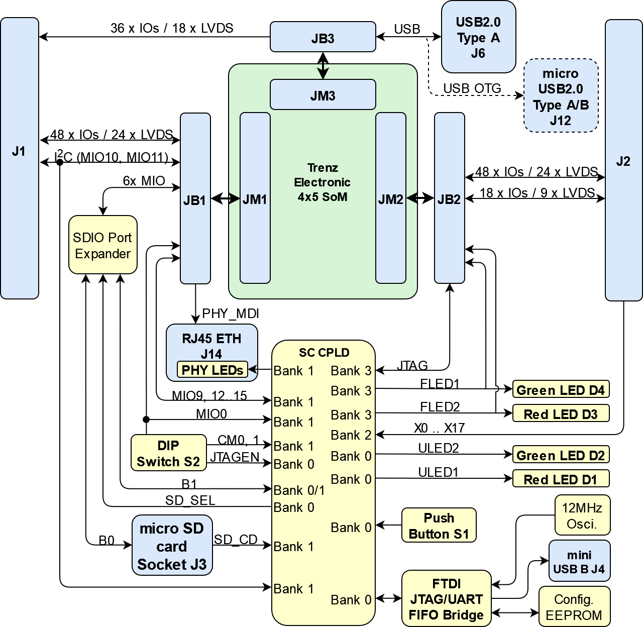
- On Board:
- USB JTAG and UART interface (FTDI FT2232H), compatible with Xilinx tools (also with many other tools)
- SDIO port expander with voltage-level translation
- 4 x User LEDs
- D1 and D2 are connected to the carrier controller, their function depends on the firmware
- D3 and D4 are connected to the 4 x 5 module B2B connector pins, and are directly controlled by the module
- 1 x User push button
- Connected to "intelligent Carrier Controller (iCC)" and can be used as module reset button. Other usage possible, actual function depend on the code loaded into iCC.
- 4A high efficiency power SoC 6 A DC-DC step-down converter with integrated inductor (Enpirion EN6347) inductor for 3.3V power supply
- 4 User DIP switches
- Enable/disable update of the "intelligent Carrier Controller"
- MIO0 (readable signal by iCC and module)
- 2 "mode" bits
- Interface:
- Trenz 4 x 5 module socket (3 x Samtec LSHM series connectors)
- Micro SD card connector - Zynq SDIO0 bootable SD port
- 2 x VG96 backplane connectors (mounting holes and solder pads)
- Mini USB connector (USB JTAG and UART interface)
- RJ45 GbE connector
- USB host connector
- Power:
- Barrel jack for 5V power supply input
- Dimension:
- 100 mm x 64.5 mm
...
| Scroll Title | ||||||||||||||||||||||||||||||||
|---|---|---|---|---|---|---|---|---|---|---|---|---|---|---|---|---|---|---|---|---|---|---|---|---|---|---|---|---|---|---|---|---|
| ||||||||||||||||||||||||||||||||
|
...
- Samtec Razor Beam™ LSHM-150 B2B connector, JB1
- Samtec Razor Beam™ LSHM-150 B2B connector, JB2
- Samtec Razor Beam™ LSHM-130 B2B connector, JB3
- Micro SD card socket with detect switch, J3
- LED indicators D1 and D2
- Mini-USB type B connector, J4
- LED indicators D3 and D4
- Configuration DIP switches, S2 (see table under "DIP switches" section)
- User push button (Reset), S1
- External connector (VG96) placeholder, J1
- External connector (VG96) placeholder, J2
- VCCIO voltage selection jumper block, J5, J8, J9 and J10 (see "Power and Power-On Sequence" section)
- Trxcom 1000Base-T Gigabit RJ45 Magjack, J14 with 4 integrated LEDs
- USB type A receptacle, J6 (optional micro USB 2.0 type A/B receptacle available, J12)
- 5V power connector jack, J13
- SD IO voltage (VCCA) selection jumper J11
...
SD IO levelshifter (U2) is used in congntion with jumper J11 to select the correct SD IO interface voltage of the SoM.
I2C Repeater
For power squenz sequence reasons the I2C bus is routed via a repater (U7) to to ensure no IOs of the SoM are driven before M3.3VOUT is up.
...
Hardware Revision History
Date | Revision | Notes | PCN | Documents |
|---|---|---|---|---|
| 2023-09-04 | 07 | See Revision changes. | ||
| 2019-09-02 | 06 | Added SD IO voltage selection jumper Further changes see PCN. | PCN-20190104 | TE0703 |
2016-09-07 | 05 | Added VCCIO Jumpers | TE0703-05 | |
- | 04 | Corrected FTDI EEPROM connection | - | TE0703-04 |
- | 03 | Added VCCIO strapping resistors | - | |
- | 02 | First series boards | - | |
- | 01 | Prototypes | - |
Hardware revision number is printed on the PCB board next to the module model number separated by the dash.
...
Date | Revision | Contributors | Description | ||||||||||||||||||||||||||
|---|---|---|---|---|---|---|---|---|---|---|---|---|---|---|---|---|---|---|---|---|---|---|---|---|---|---|---|---|---|
|
|
|
| ||||||||||||||||||||||||||
| 2022-09-23 | v.44 | Mohsen Chamanbaz |
| ||||||||||||||||||||||||||
| 2019-10-07 | v.43 | Martin Rohrmüller |
| ||||||||||||||||||||||||||
2018-06-13 | v.29 | Ali Naseri |
| ||||||||||||||||||||||||||
| 2017-02-07 | v.28 | John Hartfiel |
| ||||||||||||||||||||||||||
| 2017-11-09 | v.26 | John Hartfiel |
| ||||||||||||||||||||||||||
| 2017-02-21 | v.19 | Jan Kumann |
| ||||||||||||||||||||||||||
| 2017-02-02 | v.16 | Jan Kumann |
| ||||||||||||||||||||||||||
| 2016-12-22 | v.14 | Jan Kumann |
| ||||||||||||||||||||||||||
| 2016-12-08 | v.10 | Jan Kumann |
| ||||||||||||||||||||||||||
| 2016-12-05 | v.5 | John Hartfiel |
| ||||||||||||||||||||||||||
| 2016-09-06 | v.1 | Jan Kumann, John Hartfiel |
|
Disclaimer
| Include Page | ||||
|---|---|---|---|---|
|
...
Overview
Content Tools