Page History
...
| HTML |
|---|
<!-- Template Revision 1.66 (HTML comments will be not displayed in the document, no need to remove them. For Template/Skeleton changes, increase Template Revision number. So we can check faster, if the TRM style is up to date). --> |
| Scroll Ignore |
|---|
Download PDF version of this document. |
| HTML |
|---|
<!-- General Notes: If some section is CPLD firmware dependent, make a note and if available link to the CPLD firmware description. It's in the TE shop download area in the corresponding module -> revision -> firmware folder. --> |
...
| Scroll pdf ignore | |
|---|---|
Table of Contents
|
Overview
| HTML |
|---|
<!--
Wiki Link: Go to Base Folder of the Module or Carrier, for example : https://wiki.trenz-electronic.de/display/PD/TE0712
--> |
| Scroll Only (inline) |
|---|
Refer to https://wiki.trenz-electronic.de/display/PD/TEB0911+TRM for the current online version of this manual and other available documentation. |
The Trenz Electronic TEB0911 UltraRack+ board is an industrial-grade motherboard integrating a Xilinx Zynq UltrascaleUltraScale+ MPSoC with 4 GByte Flash memory for configuration and operation, DDR4-SDRAM SODIMM SO-DIMM socket with 64-bit wide data bus, 24 22 MGT Lanes lanes and powerful switch-mode power supplies for all on-board voltages.. The motherboard TEB0911 board exposes the pins of the Zynq MPSoC 's pins to accessible connectors and provides a whole range of on-board components to test and evaluate the Zynq UltrascaleUltraScale+ MPSoC and for developing purposes. The motherboard board is capable to be fitted to a dedicated enclosure. On , whereby on the enclosure's rear and front panel, I/O's, LVDS-pairs and MGT interfaces lanes are accessible through 6 on-board FMC connectors and other standard high-speed interfaces for , namely USB3.0, SFP+, SSD, GbE, etc.
Key Features
- Single 24V main power supply
- 2x USB3 A Connector (Superspeed Host Port (Highspeed in USB2 mode))
- Gigabit Ethernet RGMII PHY with RJ45 MegJack
- Dual SFP+ Connector (2x1 Cage)
- DDR4-SDRAM SODIMM socket (64bit bus width)
- SSD (Solid State Disk) Connector
- CAN FD Transceiver (10 Pin IDC connector and 6-pin header)
- 1x DisplayPort
- 4x On-board configuration EEPROMs (1x Microchip 24LC128-I/ST, 3x Microchip 24AA025E48T-I/OT)
- All carrier board peripherals' I²C interfaces muxed to MPSoC's I²C interface
- 6x FMC HPC Connectors
- 6x FMC Fans
- 3x Optional 4-wire PWM fan connectors
- 10 output programmable PLL clock generator Si5345A
- Quad programmable PLL clock generator SI5338A
- 1x SMA coaxial connectors for reference clock signal input
- MicroSD-Socket (bootable)
- 32 Gbit (4 GByte) on-board eMMC flash (8 banks a 4 Gbit)
- System Controller CPLD Lattice MachXO2 7000 HC
- 2x JTAG/UART header ('XMOD FTDI JTAG Adapter'-compatible) for programming MPSoC and SC CPLD
- On-board DC-DC PowerSoCs and LDOs
Additional assembly options are available for cost or performance optimization upon request.
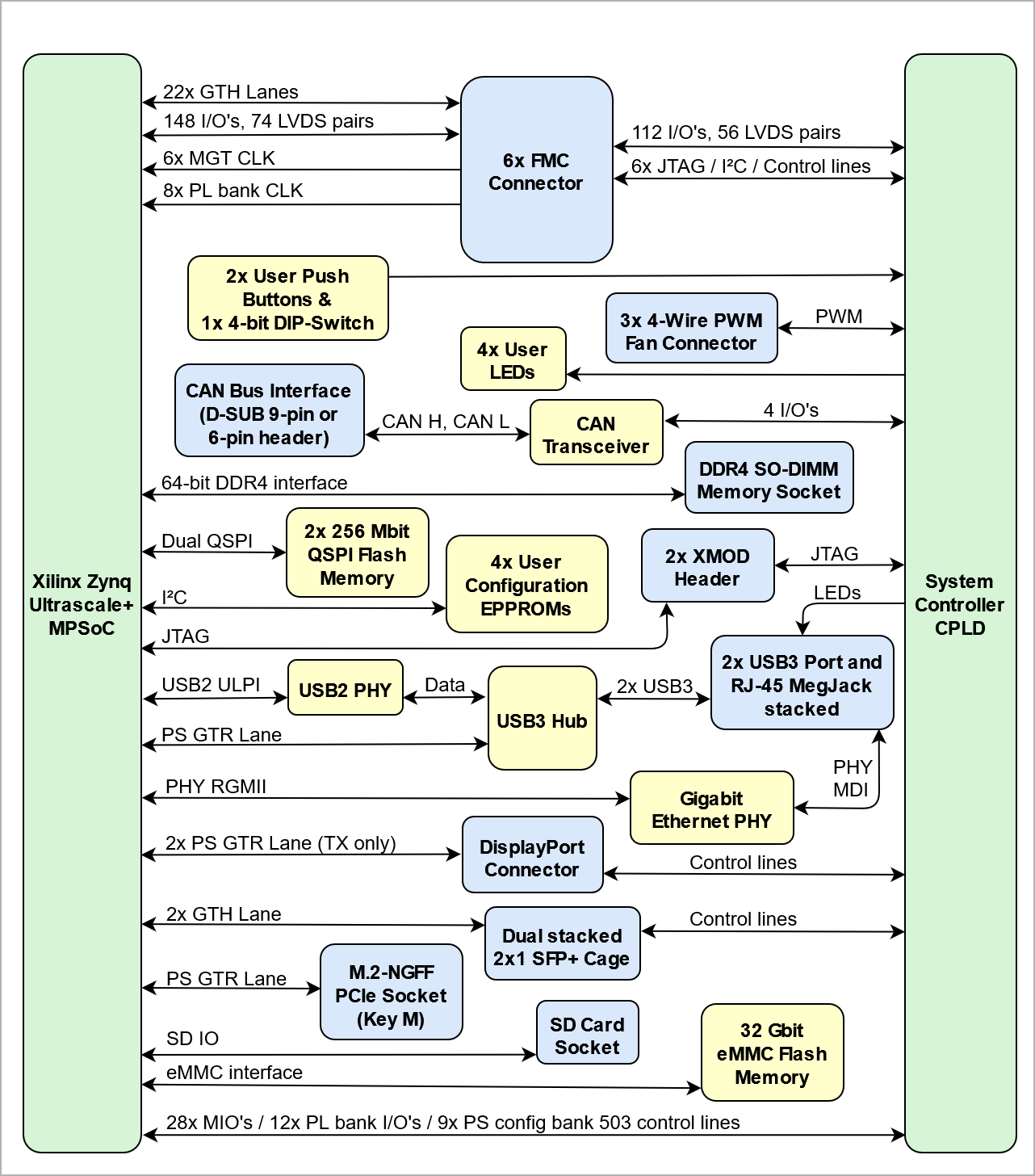
Block Diagram
Put your block diagram here...
...
| anchor | Figure_1 |
|---|---|
| title | Figure 1: TEB0911-03 block diagram |
| HTML |
|---|
<!--
Use short link the Wiki Ressource page: for example:
http://trenz.org/te0720-info
List of available short links: https://wiki.trenz-electronic.de/display/CON/Redirects
--> |
| Scroll Only (inline) |
|---|
Refer to http://trenz.org/teb0911-info for the current online version of this manual and other available documentation.
|
Key Features
- Zynq UltraScale+ MPSoC
- ZU6,ZU9 or ZU15 on 1156 Pin Package
- 64bit DDR4 SODIMM (PS connected)
- M2 PCIe SSD (1-Lane)
- eMMC (bootable)
- Dual QSPI Flash (bootable)
- System Controller(LCMXO2-7000HC)
- Power Sequencing
- IO Expander
- Configurable PLLs
- GTH/GTP Reference CLKs
Front Panel
- 4 x FMC
- 4 GTH per FMC
- 68 ZynqMP PL IO per FMC
- DisplayPort (2-Lanes)
- RJ34 ETH + Dual USB3 Combo
- Dual Stack SFP+
- SD (bootable)
- Status LEDs
Back Panel
- 2 x FMC
- 4/2 GTH
- 12 ZynqMP PL IO per FMC
- 56 SC IO per FMC
- USB JTAG/UART ZynqMP
- USB JTAG/GPIO FMC
- CAN FD (DB9 Connector)
- SMA (external CLK)
- 5polig 24V power connector
Additional assembly options are available for cost or performance optimization upon request.
Block Diagram
| Scroll Title | ||||||||||||||||||||||||||||||
|---|---|---|---|---|---|---|---|---|---|---|---|---|---|---|---|---|---|---|---|---|---|---|---|---|---|---|---|---|---|---|
| ||||||||||||||||||||||||||||||
|
Main Components
| Scroll Title | ||||||||||||||||||||||||||||||
|---|---|---|---|---|---|---|---|---|---|---|---|---|---|---|---|---|---|---|---|---|---|---|---|---|---|---|---|---|---|---|
| ||||||||||||||||||||||||||||||
|
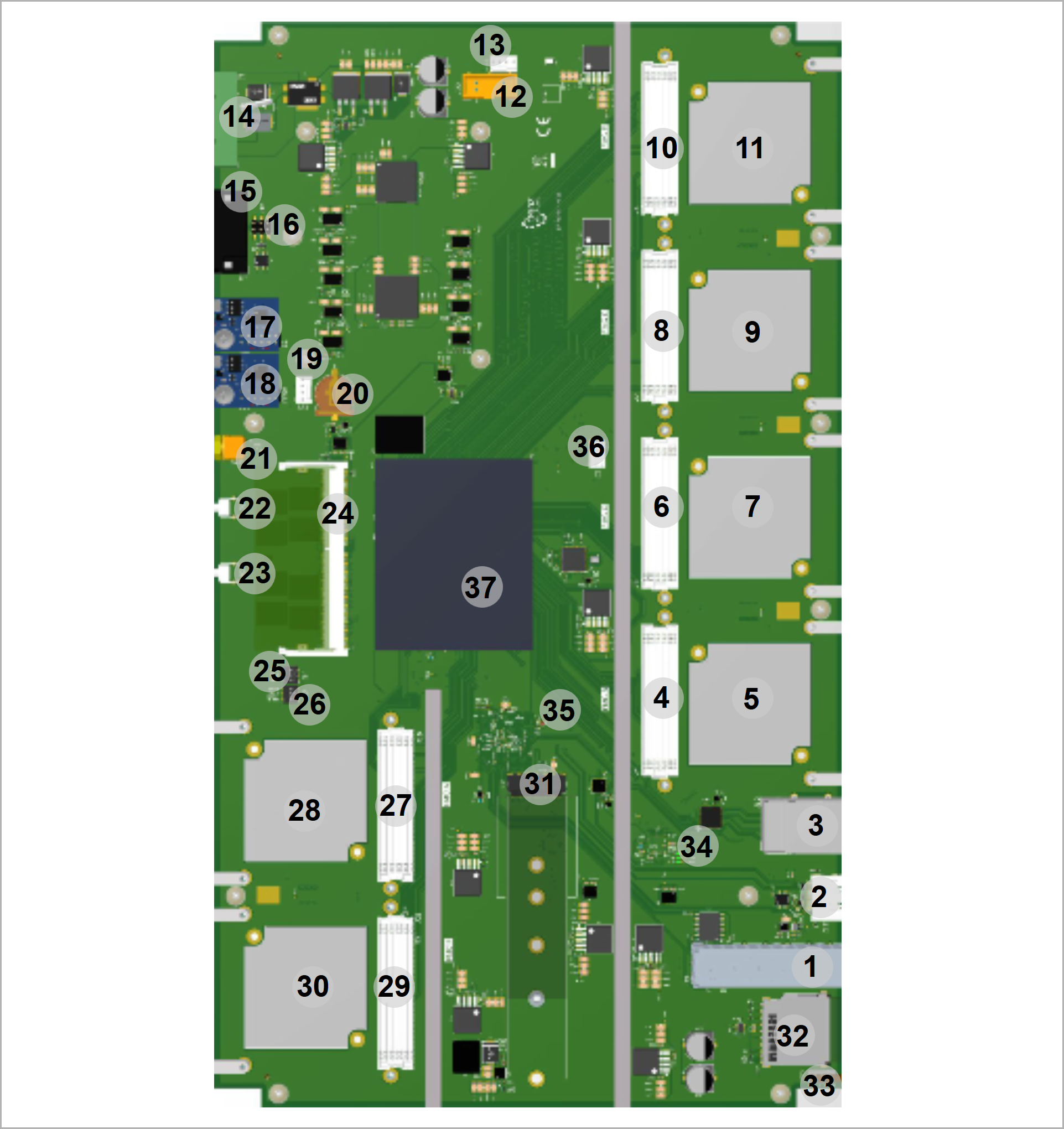
Main Components
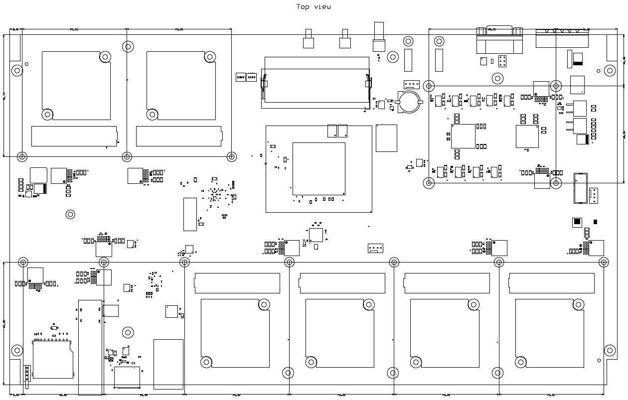
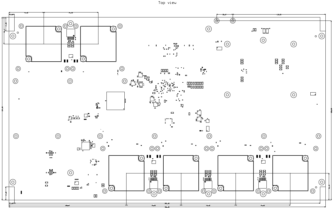
Put top and bottom pics with labels of the real PCB here...
...
| anchor | Figure_2 |
|---|---|
| title | Figure 2: TEB0911-03 main components |
...
- SFP+ 2x1 cage with integrated LED light pipes, J9
- DisplayPort connector, J12
- USB3 A 2x , RJ45 1x (stacked), J13
- FMC connector (FMC B), J4
- FMC B cooling fan, M2
- FMC connector (FMC C), J8
- FMC C cooling fan, M3
- FMC connector (FMC D), J7
- FMC D cooling fan, M4
- FMC connector (FMC E), J6
- FMC E cooling fan, M5
- I²C programming header of on-board PLL clock generator U17, J22
- 4-Wire PWM fan connector, J23
- Main Power Jack 24V, J1
- CAN bus D-SUB 9-pin male connector, J3
- CAN bus 6-pin header male, J15
- XMOD JTAG header for access to System Controller CPLD, J35
- XMOD JTAG header for access to Zynq MPSoC, J24
- 4-Wire PWM fan connector, J33
- Battery Holder CR1220, B1
- SMA coaxial connector (PLL Si5345A U17 clock input), J25
- Push Button, S1
- Push Button, S2
- DDR4 SO-DIMM socket, U3
- 4-bit DIP-switch, S4
- 4-bit DIP-switch, S3
- FMC connector (FMC A), J10
- FMC A cooling fan, M1
- FMC connector (FMC F), J21
- FMC F cooling fan, M6
- NGFF M.2 PCIe socket (Key M), U2
- SD Card socket, J11
- User LEDs (3x green, 1x red) with LED light pipe, D13 ... D16
- Green LEDs dedicated to USB3 hub U4, D17 ... D19
- Red LED indicating FPGAs 'DONE' signal, D6
- 4-Wire PWM fan connector, J2
- Xilinx Zynq Ultrascale+ MPSoC, U1
Initial Delivery State
Storage device name | Content | Notes |
|---|---|---|
| User configuration EEPROMs (1x Microchip 24LC128-I/ST, 3x Microchip 24AA025E48T-I/OT) | Empty | Not programmed |
| USB3 HUB Configuration EEPROM (Microchip 24LC128-I/ST) | Empty | Not programmed |
| Si5338A programmable PLL NVM OTP | Empty | Not programmed |
| Si5345A programmable PLL NVM OTP | Empty | Not programmed |
| eMMC Flash memory | Empty | Not programmed |
| 2x QSPI Flash memory | Empty | Not programmed |
Table 1: Initial delivery state of programmable devices on the module.
Boot Process
For the boot process prior to powering up the board settings must be done via DIP-Switch S3-3 and S3-4. Four boot modes can be selected:
| S3-3 (SC_SW1) | S3-4 (SC_SW2) | MIO Location | Description | Notes |
|---|---|---|---|---|
| OFF | OFF | MIO[43:38] | SD1 Boot Mode (SD-Card on J11) | Supports SD 2.0. |
| OFF | ON | MIO[29:26] | PJTAG0 | PS JTAG connection 0 option. |
| ON | OFF | MIO[12:0] | QSPI32 | 32-bit addressing, configured with dual on-board QSPI Flash Memory. |
| ON | ON | - | JTAG | Dedicated PS interface. |
Table 2: Available boot modes of the on-board Zynq MPSoC
Refer also to the documentation of the SC CPLD firmware of the TEB0911 board, section 'boot mode'.
Signals, Interfaces and Pins
...
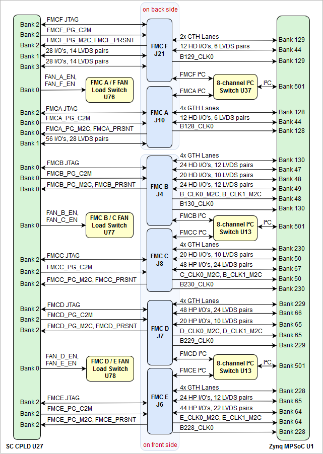
The TEB0911 Ultrarack+ offers 6 FMC (FPGA Mezzanine Card) connectors which provides as an ANSI/VITA 57.1 standard a modular interface to the MPSoCs FPGA and exposes numerous of its I/O pins and MGT Lanes lanes for use by other mezzanine modules and expansion cards.
...
| Scroll Title | |||||||||||||||||||||||||||||||||
|---|---|---|---|---|---|---|---|---|---|---|---|---|---|---|---|---|---|---|---|---|---|---|---|---|---|---|---|---|---|---|---|---|---|
| |||||||||||||||||||||||||||||||||
|
| HTML |
|---|
<!-- MGT lanes should be listed separately, as they are more specific than just general I/Os. --> |
Following tables contains information about the interfaces, I/O's, clock and VCCIO sources available on the FMC connectors A - F:
Anchor FMC A FMC A
FMC A
FMC A Interfaces:
| FMC | Interfaces | I/O Signal Count | LVDS-pairs count | Connected to | VCCO bank Voltage | Notes |
|---|---|---|---|---|---|---|
J10 (FMC A) | I/O | 12 | 6 | Bank 44 HD | FMCAF_1V8 | - |
| 4656 | 28 | SC CPLD U27 Bank 1 | FMCAF_1V8 | - | ||
| I²C | 2 | - | I²C-Switch U37 | - | Muxed to MIO Bank 501 I²C Inteface | |
| JTAG | 4 | - | SC CPLD U27 Bank 2 | 3.3VSB | - | |
| MGT | - | 8 (4 x RX/TX) | Bank 128 GTH | - | 4x MGT lanes | |
| Clock Input | - | 1 | Bank 128 GTH | - | 1x Reference clock input to MGT bank | |
| Control Signals | 3 | - | SC CPLD U27 Bank 0 | 3.3VSB | 'FMCA_PG_C2M', 'FMCA_PG_M2C', 'FMCA_PRSNT' |
Table 3: FMC A connector interfaces
FMC A MGT Lanes:
| FMC | MGT Lane | Bank | Type | Signal Schematic Name | FMC Connector Pin | FPGA Pin |
|---|---|---|---|---|---|---|
J10 (FMC A) | 0 | 128 | GTH |
| J10-C6 | MGTHRXP0_128, T33 |
| 1 | 128 | GTH |
| J10-A2 | MGTHRXP1_128, P33 | |
| 2 | 128 | GTH |
| J10-A6 | MGTHRXP2_128, N31 | |
| 3 | 128 | GTH |
| J10-A10 | MGTHRXP3_128, M33 |
Table 4: FMC A connector MGT lanes
FMC A Clock Signals:
| FMC | Signal Schematic Name | Bank | FMC Connector Pin | FPGA Pin | Notes |
|---|---|---|---|---|---|
J10 (FMC A) |
| 128 | J10-D4 | MGTREFCLK0P_128, R27 | Supplied by attached module |
Table 5: FMC A connector clock signal input
FMC A VCC/VCCIO:
| FMC | Available VCC/VCCIO | FMC Connector Pin | Source | Notes |
|---|---|---|---|---|
J10 (FMC A) | FMCA_3V3 | J10-D36 | DCDC U32, | Enable by SC CPLD U27, bank 2, pin Y18 |
| 3V3SB | J10-D32 | DCDC U50, max. cur.: 1A | not dedicated for FMC connectors | |
| 12V_FMC_AF | J10-C35 | DCDC U51, | - | |
| FMCAF_1V8 | J10-H40 | DCDC U39, | Enable by SC CPLD U27, bank 2, pin W19 |
Table 6: FMC A connector available VCC/VCCIO
FMC A Cooling Fan:
| FMC | Fan Designator | Enable Signal | Notes |
|---|---|---|---|
J10 (FMC A) | M1 | Enable by SC CPLD U27, bank 2, pin Y19 | - |
Table 7: FMC A connector cooling fan
Anchor FMC F FMC F
FMC F
FMC F Interfaces:
| FMC | Interfaces | I/O Signal Count | LVDS-pairs count | Connected to | VCCO bank Voltage | Notes |
|---|---|---|---|---|---|---|
J21 (FMC F) | I/O | 12 | 6 | Bank 44 HD | FMCAF_1V8 | - |
| 28 | 14 | SC CPLD U27 Bank 1 | FMCAF_1V8 | - | ||
| 6828 | 3414 | SC CPLD U27 Bank 3 | FMCAF_1V8 | - | ||
| I²C | 2 | - | I²C-Switch U37 | - | Muxed to MIO Bank 501 I²C Inteface | |
| JTAG | 4 | - | SC CPLD U27 Bank 2 | 3.3VSB | - | |
| MGT | - | 4 (2 x RX/TX) | Bank 129 GTH | - | 2x MGT lanes | |
| Clock Input | - | 1 | Bank 129 GTH | - | 1x Reference clock input to MGT bank | |
| Control Signals | 3 | - | SC CPLD U27 Bank 2 | 3.3VSB | 'FMCF_PG_C2M', 'FMCF_PG_M2C', 'FMCF_PRSNT' |
Table 8: FMC F connector interface
FMC F MGT Lanes:
| FMC | MGT Lane | Bank | Type | Signal Schematic Name | FMC Connector Pin | FPGA Pin |
|---|---|---|---|---|---|---|
J21 (FMC F) | 0 | 129 | GTH |
| J21-C6 | MGTHRXP0_129, L31 |
| 1 | 129 | GTH |
| J21-A2 | MGTHRXP1_129, K33 |
Table 9: FMC F connector MGT lanes
FMC F Clock Signals:
| FMC | Signal Schematic Name | Bank | FMC Connector Pin | FPGA Pin | Notes |
|---|---|---|---|---|---|
J21 (FMC F) |
| 129 | J21-D4 | MGTREFCLK0P_129, L27 | Supplied by attached module |
Table 10: FMC F connector clock signal input
FMC F VCC/VCCIO:
| FMC | Available VCC/VCCIO | FMC Connector Pin | Source | Notes |
|---|---|---|---|---|
J21 (FMC F) | FMCF_3V3 | J21-D36 | DCDC U42, | Enable by SC CPLD U27, bank 2, pin Y10 |
| 3V3SB | J21-D32 | DCDC U50, max. cur.: 1A | not dedicated for FMC connectors | |
| 12V_FMC_AF | J21-C35 | DCDC U51, | - | |
| FMCAF_1V8 | J21-H40 | DCDC U39, | Enable by SC CPLD U27, bank 2, pin W19 |
Table 11: FMC F connector available VCC/VCCIO
FMC F Cooling Fan:
| FMC | Fan Designator | Enable Signal | Notes |
|---|---|---|---|
J21 (FMC F) | M6 | Enable by SC CPLD U27, bank 2, pin W18 | - |
Table 12: FMC F connector cooling fan
Anchor FMC B FMC B
FMC B
FMC B Interfaces:
| FMC | Interfaces | I/O Signal Count | LVDS-pairs count | Connected to | VCCO bank Voltage | Notes |
|---|---|---|---|---|---|---|
J4 (FMC B) | I/O | 24 | 12 | Bank 47 HD | FMCBC_1V8 | - |
| 20 | 10 | Bank 48 HD | FMCBC_1V8 | - | ||
| 24 | 12 | Bank 49 HD | FMCBC_1V8 | - | ||
| I²C | 2 | - | I²C-Switch U13 | - | Muxed to MIO Bank 501 I²C Inteface | |
| JTAG | 4 | - | SC CPLD U27 Bank 0 | 3.3VSB | - | |
| MGT | - | 8 (4 x RX/TX) | Bank 130 GTH | - | 4x MGT lanes | |
| Clock Input | - | 2 | Bank 48 HD | - | 2x Reference clock inputs to PL bank | |
| - | 1 | Bank 130 GTH | - | 1x Reference clock input to MGT bank | ||
| Control Signals | 3 | - | SC CPLD U27 Bank 0 | 3.3VSB | 'FMCB_PG_C2M', 'FMCB_PG_M2C', 'FMCB_PRSNT' |
Table 13: FMC B connector interfaces
FMC B MGT Lanes:
| FMC | MGT Lane | Bank | Type | Signal Schematic Name | FMC Connector Pin | FPGA Pin |
|---|---|---|---|---|---|---|
J4 (FMC B) | 3 | 130 | GTH |
| J4-C6 | MGTHRXP3_130, B33 |
| 2 | 130 | GTH |
| J4-A2 | MGTHRXP2_130, C31 | |
| 1 | 130 | GTH |
| J4-A6 | MGTHRXP1_130, D33 | |
| 0 | 130 | GTH |
| J4-A10 | MGTHRXP0_130, E31 |
Table 14: FMC B connector MGT lanes
FMC B Clock Signals:
| FMC | Signal Schematic Name | Bank | FMC Connector Pin | FPGA Pin | Notes |
|---|---|---|---|---|---|
J4 (FMC B) |
| 130 | J4-D4 | MGTREFCLK0P_130, G27 | Supplied by attached module |
| 48 HD | J4-H4 | IO_L6P_HDGC_48, F17 | Supplied by attached module | |
| 48 HD | J4-G2 | IO_L5P_HDGC_48, G18 | Supplied by attached module |
Table 15: FMC B connector clock signal input
FMC B VCC/VCCIO:
| FMC | Available VCC/VCCIO | FMC Connector Pin | Source | Notes |
|---|---|---|---|---|
J4 (FMC B) | FMCB_3V3 | J4-D36 | DCDC U33, | Enable by SC CPLD U27, bank 0, pin G11 |
| 3V3SB | J4-D32 | DCDC U50, max. cur.: 1A | not dedicated for FMC connectors | |
| 12V | J4-C35 | DCDC U82, | not dedicated for FMC connectors | |
| FMCBC_1V8 | J4-H40 | DCDC U40, | Enable by SC CPLD U27, bank 0, pin A3 |
Table 16: FMC B connector available VCC/VCCIO
FMC B Cooling Fan:
| FMC | Fan Designator | Enable Signal | Notes |
|---|---|---|---|
J4 (FMC B) | M2 | Enable by SC CPLD U27, bank 0, pin A2 | - |
Table 17: FMC B connector cooling fan
Anchor FMC C FMC C
FMC C
FMC C Interfaces:
| FMC | Interfaces | I/O Signal Count | LVDS-pairs count | Connected to | VCCO bank Voltage | Notes |
|---|---|---|---|---|---|---|
J8 (FMC C) | I/O | 20 | 10 | Bank 50 HD | FMCBC_1V8 | - |
| 6848 | 3424 | Bank 67 HP | FMCBC_1V8 | - | ||
| I²C | 2 | - | I²C-Switch U13 | - | Muxed to MIO Bank 501 I²C Inteface | |
| JTAG | 4 | - | SC CPLD U27 Bank 2 | 3.3VSB | - | |
| MGT | - | 8 (4 x RX/TX) | Bank 230 GTH | - | 4x MGT lanes | |
| Clock Input | - | 2 | Bank 50 HD | - | 2x Reference clock inputs to PL bank | |
| - | 1 | Bank 230 GTH | - | 1x Reference clock input to MGT bank | ||
| Control Signals | 3 | - | SC CPLD U27 Bank 2 | 3.3VSB | 'FMCC_PG_C2M', 'FMCC_PG_M2C', 'FMCC_PRSNT' |
Table 18: FMC C connector interfaces
FMC C MGT Lanes:
| FMC | MGT Lane | Bank | Type | Signal Schematic Name | FMC Connector Pin | FPGA Pin |
|---|---|---|---|---|---|---|
J8 (FMC C) | 3 | 230 | GTH |
| J8-C6 | MGTHRXP3_230, A4 |
| 2 | 230 | GTH |
| J8-A2 | MGTHRXP2_230, B2 | |
| 1 | 230 | GTH |
| J8-A6 | MGTHRXP1_230, C4 | |
| 0 | 230 | GTH |
| J8-A10 | MGTHRXP0_230, D2 |
Table 19: FMC C connector MGT lanes
FMC C Clock Signals:
| FMC | Signal Schematic Name | Bank | FMC Connector Pin | FPGA Pin | Notes |
|---|---|---|---|---|---|
J8 (FMC C) |
| 230 | J8-D4 | MGTREFCLK0P_230, C8 | Supplied by attached module |
| 50 HD | J8-H4 | IO_L7P_HDGC_50, J12 | Supplied by attached module | |
| 50 HD | J8-G2 | IO_L8P_HDGC_50, H13 | Supplied by attached module |
Table 20: FMC C connector clock signal input
FMC C VCC/VCCIO:
| FMC | Available VCC/VCCIO | FMC Connector Pin | Source | Notes |
|---|---|---|---|---|
J8 (FMC C) | FMCC_3V3 | J8-D36 | DCDC U34, | Enable by SC CPLD U27, bank 0, pin E11 |
| 3V3SB | J8-D32 | DCDC U50, max. cur.: 1A | not dedicated for FMC connectors | |
| 12V | J8-C35 | DCDC U82, | not dedicated for FMC connectors | |
| FMCBC_1V8 | J8-H40 | DCDC U40, | Enable by SC CPLD U27, bank 0, pin A3 |
Table 21: FMC C connector available VCC/VCCIO
FMC C Cooling Fan:
| FMC | Fan Designator | Enable Signal | Notes |
|---|---|---|---|
J8 (FMC C) | M3 | Enable by SC CPLD U27, bank 0, pin B3 | - |
Table 22: FMC C connector cooling fan
Anchor FMC D FMC D
FMC D
FMC D Interfaces:
| FMC | Interfaces | I/O Signal Count | LVDS-pairs count | Connected to | VCCO bank Voltage | Notes |
|---|---|---|---|---|---|---|
J7 (FMC D) | I/O | 20 | 10 | Bank 65 HP | FMCDE_1V8 | - |
| 48 | 24 | Bank 66 HP | FMCDE_1V8 | - | ||
| I²C | 2 | - | I²C-Switch U13 | - | Muxed to MIO Bank 501 I²C Inteface | |
| JTAG | 4 | - | SC CPLD U27 Bank 2 | 3.3VSB | - | |
| MGT | - | 8 (4 x RX/TX) | Bank 229 GTH | - | 4x MGT lanes | |
| Clock Input | - | 2 | Bank 65 HP | - | 2x Reference clock inputs to PL bank | |
| - | 1 | Bank 229 GTH | - | 1x Reference clock input to MGT bank | ||
| Control Signals | 3 | - | SC CPLD U27 Bank 2 | 3.3VSB | 'FMCD_PG_C2M', 'FMCD_PG_M2C', 'FMCD_PRSNT' |
Table 23: FMC D connector interfaces
FMC D MGT Lanes:
| FMC | MGT Lane | Bank | Type | Signal Schematic Name | FMC Connector Pin | FPGA Pin |
|---|---|---|---|---|---|---|
J7 (FMC D) | 3 | 229 | GTH |
| J7-C6 | MGTHRXP3_229, F2 |
| 2 | 229 | GTH |
| J7-A2 | MGTHRXP2_229, H2 | |
| 1 | 229 | GTH |
| J7-A6 | MGTHRXP1_229, J4 | |
| 0 | 229 | GTH |
| J7-A10 | MGTHRXP0_229, K2 |
Table 24: FMC D connector MGT lanes
FMC D Clock Signals:
| FMC | Signal Schematic Name | Bank | FMC Connector Pin | FPGA Pin | Notes |
|---|---|---|---|---|---|
J7 (FMC D) |
| 229 | J7-D4 | MGTREFCLK0P_229, G8 | Supplied by attached module |
| 65 HP | J7-H4 | IO_L14P_T2L_N2_GC_65, AG5 | Supplied by attached module | |
| 65 HP | J7-G2 | IO_L13P_T2L_N0_GC_QBC_65, AE5 | Supplied by attached module |
Table 25: FMC D connector clock signal input
FMC D VCC/VCCIO:
| FMC | Available VCC/VCCIO | FMC Connector Pin | Source | Notes |
|---|---|---|---|---|
J7 (FMC D) | FMCD_3V3 | J7-D36 | DCDC U35, | Enable by SC CPLD U27, bank 0, pin F8 |
| 3V3SB | J7-D32 | DCDC U50, max. cur.: 1A | not dedicated for FMC connectors | |
| 12V | J7-C35 | DCDC U82, | not dedicated for FMC connectors | |
| FMCDE_1V8 | J7-H40 | DCDC U41, | Enable by SC CPLD U27, bank 0, pin C5 |
Table 26: FMC D connector available VCC/VCCIO
FMC D Cooling Fan:
| FMC | Fan Designator | Enable Signal | Notes |
|---|---|---|---|
J7 (FMC D) | M4 | Enable by SC CPLD U27, bank 0, pin D7 | - |
Table 27: FMC D connector cooling fan
Anchor FMC E FMC E
FMC E
FMC E Interfaces:
| FMC | Interfaces | I/O Signal Count | LVDS-pairs count | Connected to | VCCO bank Voltage | Notes |
|---|---|---|---|---|---|---|
J6 (FMC E) | I/O | 24 | 12 | Bank 65 HP | FMCDE_1V8 | - |
| 44 | 22 | Bank 64 HP | FMCDE_1V8 | - | ||
| I²C | 2 | - | I²C-Switch U13 | - | Muxed to MIO Bank 501 I²C Inteface | |
| JTAG | 4 | - | SC CPLD U27 Bank 2 | 3.3VSB | - | |
| MGT | - | 8 (4 x RX/TX) | Bank 228 GTH | - | 4x MGT lanes | |
| Clock Input | - | 2 | Bank 64 HP | - | 2x Reference clock inputs to PL bank | |
| - | 1 | Bank 228 GTH | - | 1x Reference clock input to MGT bank | ||
| Control Signals | 3 | - | SC CPLD U27 Bank 2 | 3.3VSB | 'FMCE_PG_C2M', 'FMCE_PG_M2C', 'FMCE_PRSNT' |
Table 28: FMC E connector interfaces
FMC E MGT Lanes:
| FMC | MGT Lane | Bank | Type | Signal Schematic Name | FMC Connector Pin | FPGA Pin |
|---|---|---|---|---|---|---|
J6 (FMC E) | 3 | 228 | GTH |
| J6-C6 | MGTHRXP3_228, L4 |
| 2 | 228 | GTH |
| J6-A2 | MGTHRXP2_228, M2 | |
| 1 | 228 | GTH |
| J6-A6 | MGTHRXP1_228, P2 | |
| 0 | 228 | GTH |
| J6-A10 | MGTHRXP0_228, T2 |
Table 29: FMC E connector MGT lanes
FMC E Clock Signals:
| FMC | Signal Schematic Name | Bank | FMC Connector Pin | FPGA Pin | Notes |
|---|---|---|---|---|---|
J6 (FMC E) |
| 228 | J6-D4 | MGTREFCLK0P_228, L8 | Supplied by attached module |
| 64 HP | J6-H4 | IO_L12P_T1U_N10_GC_64, AL8 | Supplied by attached module | |
| 64 HP | J6-G2 | IO_L11P_T1U_N8_GC_64, AK8 | Supplied by attached module |
Table 30: FMC E connector clock signal input
FMC E VCC/VCCIO:
| FMC | Available VCC/VCCIO | FMC Connector Pin | Source | Notes |
|---|---|---|---|---|
J6 (FMC E) | FMCE_3V3 | J6-D36 | DCDC U36, | Enable by SC CPLD U27, bank 0, pin E8 |
| 3V3SB | J6-D32 | DCDC U50, max. cur.: 1A | not dedicated for FMC connectors | |
| 12V | J6-C35 | DCDC U82, | not dedicated for FMC connectors | |
| FMCDE_1V8 | J6-H40 | DCDC U41, | Enable by SC CPLD U27, bank 0, pin C5 |
Table 31: FMC E connector available VCC/VCCIO
FMC E Cooling Fan:
| FMC | Fan Designator | Enable Signal | Notes |
|---|---|---|---|
J6 (FMC E) | M5 | Enable by SC CPLD U27, bank 0, pin D6 | - |
Table 32: FMC E connector cooling fan
XMOD JTAG Interface
JTAG access to the Zynq MPSoC and SC CPLD is provided through XMOD header J24 and J35:
| Scroll Title | |||||||||||||||||||||||||||||||||
|---|---|---|---|---|---|---|---|---|---|---|---|---|---|---|---|---|---|---|---|---|---|---|---|---|---|---|---|---|---|---|---|---|---|
| |||||||||||||||||||||||||||||||||
|
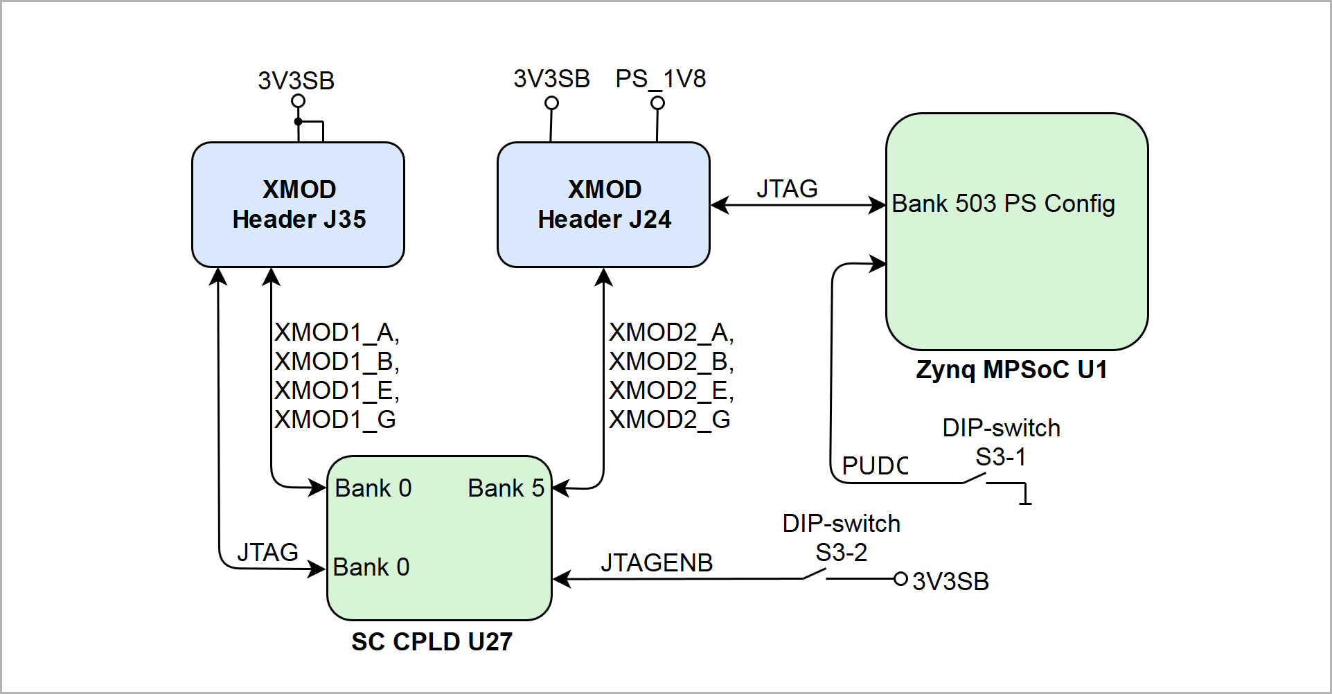
Signal Assignment of XMOD header J24 and J35
...
The JTAG interfaces of the TEB0911 UltraRack board can accessed with the XMOD-FT2232H adapter-board TE0790. The on-board devices Zynq MPSoC U1 and SC CPLD U27 can be programmed via USB2.0 interface of the TE0790 boardprogrammer.
XMOD-Header J24 is designated to program the Zynq Ultrascale+ MPSoC via USB interface, the 4 GPIO/UART pins (XMOD2_A/B/E/G) of this header are routed to the System Controller CPLD U27.
XMOD-Header J35 is designated to program the System Controller CPLD U27 via USB interface, the 4 GPIO/UART pins (XMOD1_A/B/E/G) of this header are also routed to the System Controller CPLD U27.
To program the System Controller CPLD, the JTAG interface of this devices have to be activated by DIP-switch S3-2. J35 JTAG is used for FMC JTAG, is JTAGENB is low (see CPLD Firmware).
When using XMOD FTDI JTAG Adapter TE0790, the adapter-board's VCC and VCCIO on both headers J24 and J35 will be sourced by the on-board supply voltages. Set the XMOD DIP-switch with the setting:
...
| Note |
|---|
Use Xilinx compatible TE0790 adapter board (designation TE-0790-xx with out without 'L') to program the Xilinx Zynq devices. The TE0790 adapter board's CPLD have to be configured with the Standard variant of the firmware. Refer to the TE0790 Resources Site for further information and firmware download. |
...
| Scroll Title | ||||||||||||||||||||||||||||||||
|---|---|---|---|---|---|---|---|---|---|---|---|---|---|---|---|---|---|---|---|---|---|---|---|---|---|---|---|---|---|---|---|---|
| ||||||||||||||||||||||||||||||||
|
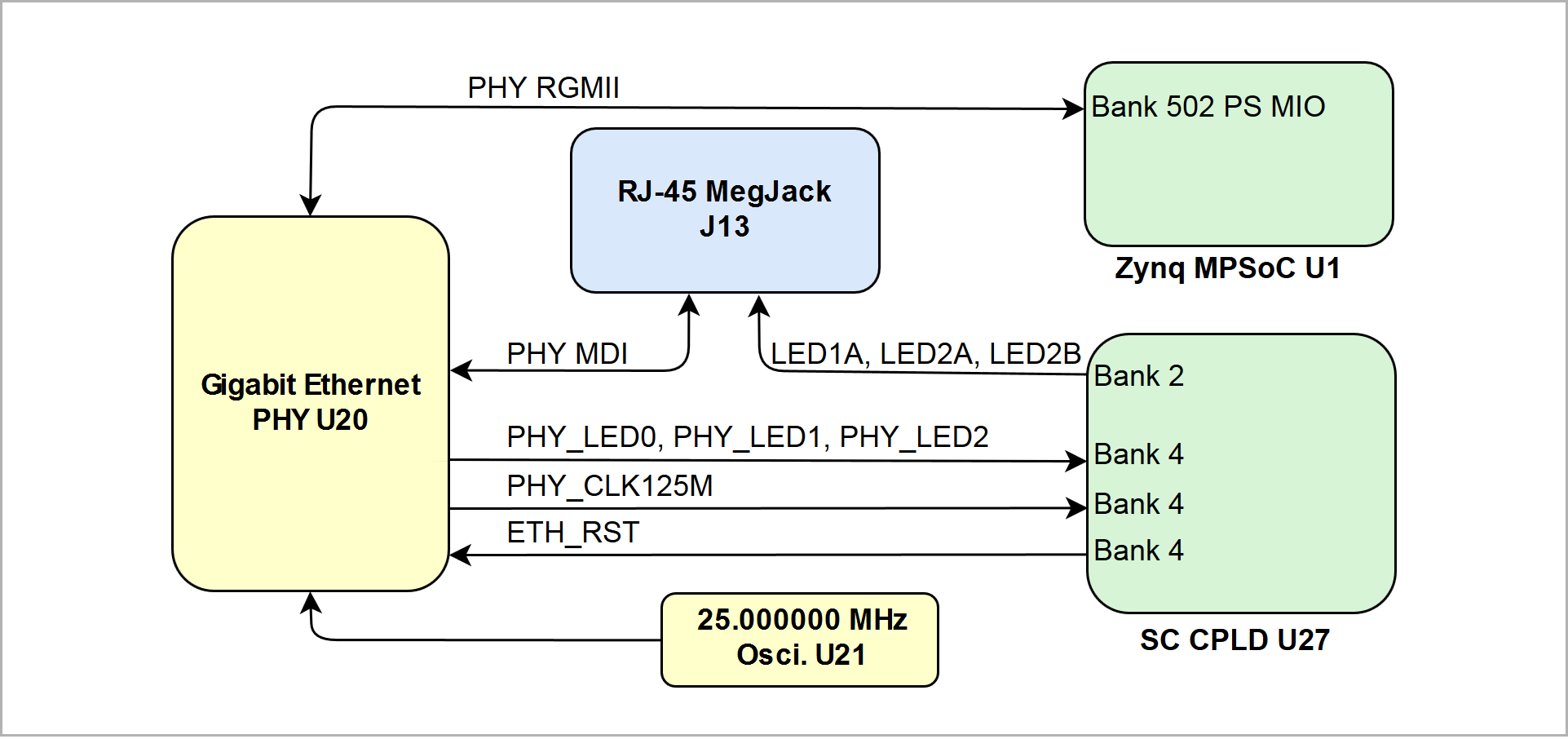
Following table describes the signals and control lines of the Gigabit Ethernet interface of the board:
| PHY Pin | Connected to | Notes |
|---|---|---|
| MDC/MDIO | PS bank 502 MIO76, MIO77 | - |
| PHY LED0..2 | SC CPLD U27, bank 4, pin L5, L1, K1 | see schematic for details, forwarded to RJ45 GbE MagJack J7 |
| PHY_CLK125M | SC CPLD U27, bank 4, pin K2 | 125 MHz Ethernet PHY clock out |
| CONFIG | pulled up to PS_1V8 | Configuration of PHY address LSB and VDDO level |
| RESETn | SC CPLD U27, bank 4, pin L6 | Active low reset line |
| RGMII | PS bank 502 MIO64 ... MIO75 | Reduced Gigabit Media Independent Interface |
| SGMII | - | Serial Gigabit Media Independent Interface |
| MDI | RJ45 GbE MagJack J13 | Media Dependent Interface |
...
| Scroll Title | ||||||||||||||||||||||||||||||||||
|---|---|---|---|---|---|---|---|---|---|---|---|---|---|---|---|---|---|---|---|---|---|---|---|---|---|---|---|---|---|---|---|---|---|---|
| ||||||||||||||||||||||||||||||||||
|
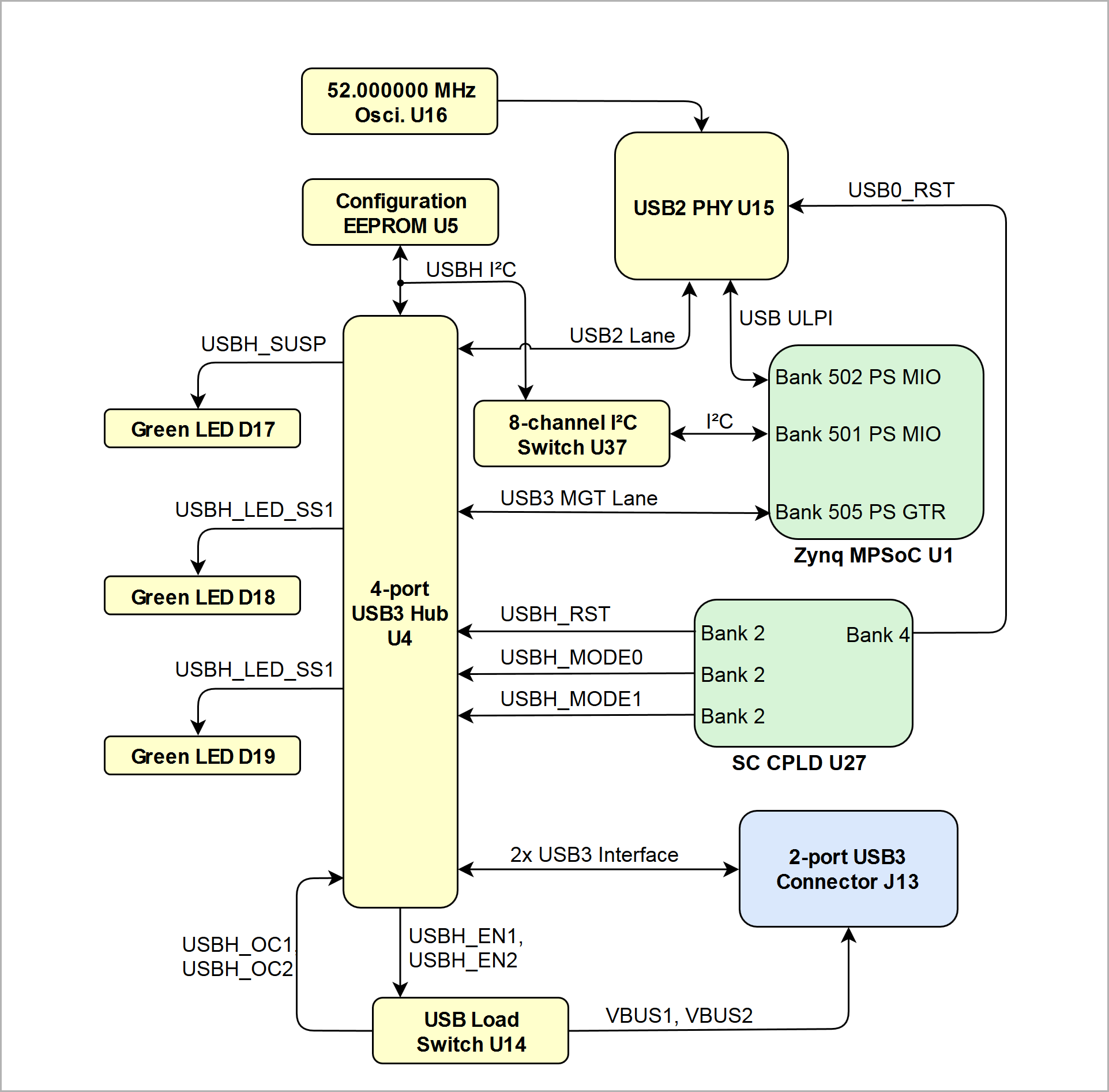
The 4-port USB3 hub is connected to the Zynq MPSoC's PS GTR bank, the USB2 PHY is connected to the PS MIO bank 502:
...
| Scroll Title | |||||||||||||||||||||||||||||||||||||
|---|---|---|---|---|---|---|---|---|---|---|---|---|---|---|---|---|---|---|---|---|---|---|---|---|---|---|---|---|---|---|---|---|---|---|---|---|---|
| |||||||||||||||||||||||||||||||||||||
|
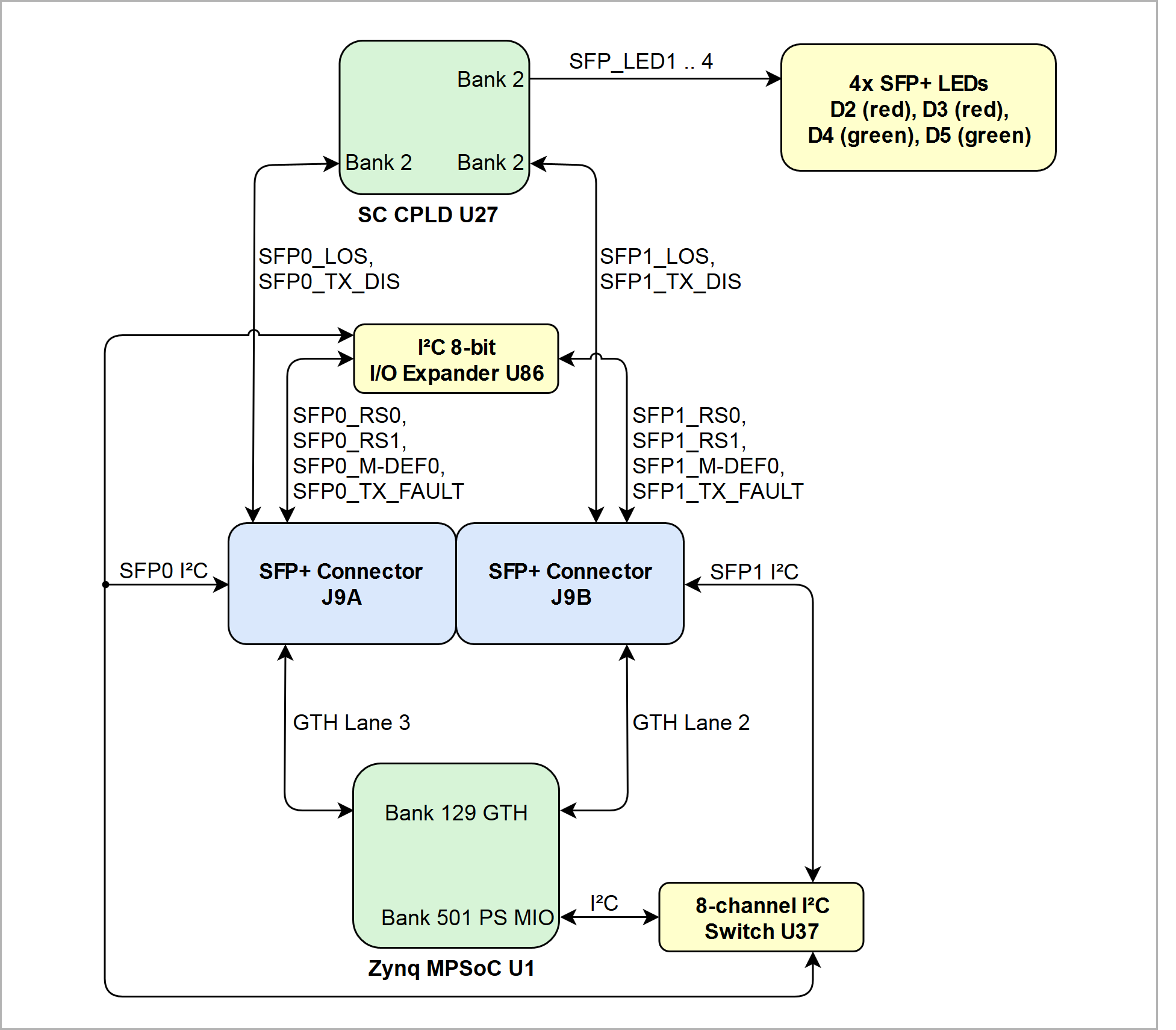
| Connector | Interface | Signal Schematic Name | Connected to | Logic | Notes |
|---|---|---|---|---|---|
SFP+ J9A | MGT Lane |
| MGTHTXP3_129, G31 | TX: Output RX: Input | Multi gigabit highspeed data lane |
| I²C |
| 8-channel I²C-switch U37 | BiDir | 2-wire Serial Interface | |
| Control Lines |
| I²C 8-bit I/O Port-Expander U86 | Output, low active | Full RX bandwidth | |
| Output, low active | Reduced RX bandwidth | |||
| Input, low active | Module present / not present | |||
| Input, high active | Fault / Normal Operation | |||
| SC CPLD U27, bank 2, pin V8 | Input, high active | Loss of receiver signal | ||
| SC CPLD U27, bank 2, pin Y7 | Output, low active | SFP Enabled / Disabled | ||
SFP+ J9B | MGT Lane |
| MGTHTXP2_129, H29 | TX: Output RX: Input | Multi gigabit highspeed |
| I²C |
| 8-channel I²C-switch U37 | Bidir | 2-wire Serial Interface | |
| Control Lines |
| I²C 8-bit I/O Port-Expander U86 | Output, low active | Full RX bandwidth | |
| Output, low active | Reduced RX bandwidth | |||
| Input, low active | Module present / not present | |||
| Input, high active | Fault / Normal Operation | |||
| SC CPLD U27, bank 2, pin W7 | Input, high active | Loss of receiver signal | ||
| SC CPLD U27, bank 2, pin V7 | Output. low active | SFP Enabled / Disabled |
...
| Scroll Title | |||||||||||||||||||||||||||||||||||
|---|---|---|---|---|---|---|---|---|---|---|---|---|---|---|---|---|---|---|---|---|---|---|---|---|---|---|---|---|---|---|---|---|---|---|---|
| |||||||||||||||||||||||||||||||||||
| 642 | revision | 1
|
| Scroll Only |
|---|
|

| Connector | Interface | Signal Schematic Name | Connected to | Notes |
|---|---|---|---|---|
M.2-NGFF PCIe Socket U2 | MGT Lane |
| PS_MGTRTXP0_505, AB29 | Multi gigabit highspeed TX: Output RX: Input |
| Clock Input |
| Quad programmable PLL clock generator U12, CLK0 | Reference clock signal | |
| Control Lines |
| SC CPLD U27, bank 2, pin AA13 | LED, Output, High active | |
| SC CPLD U27, bank 2, pin AA12 | PCIe sleep state, Input, Low active | ||
| SC CPLD U27, bank 2, pin AA11 | PCIe reset input, Input, Low active | ||
| SC CPLD U27, bank 2, pin AB11 | PCIe Link reactivation, Input, Low active | ||
| connect to GND | PCIe Clock Request, Low active |
...
| Scroll Title | ||||||||||||||||||||||||||||||||
|---|---|---|---|---|---|---|---|---|---|---|---|---|---|---|---|---|---|---|---|---|---|---|---|---|---|---|---|---|---|---|---|---|
| ||||||||||||||||||||||||||||||||
|
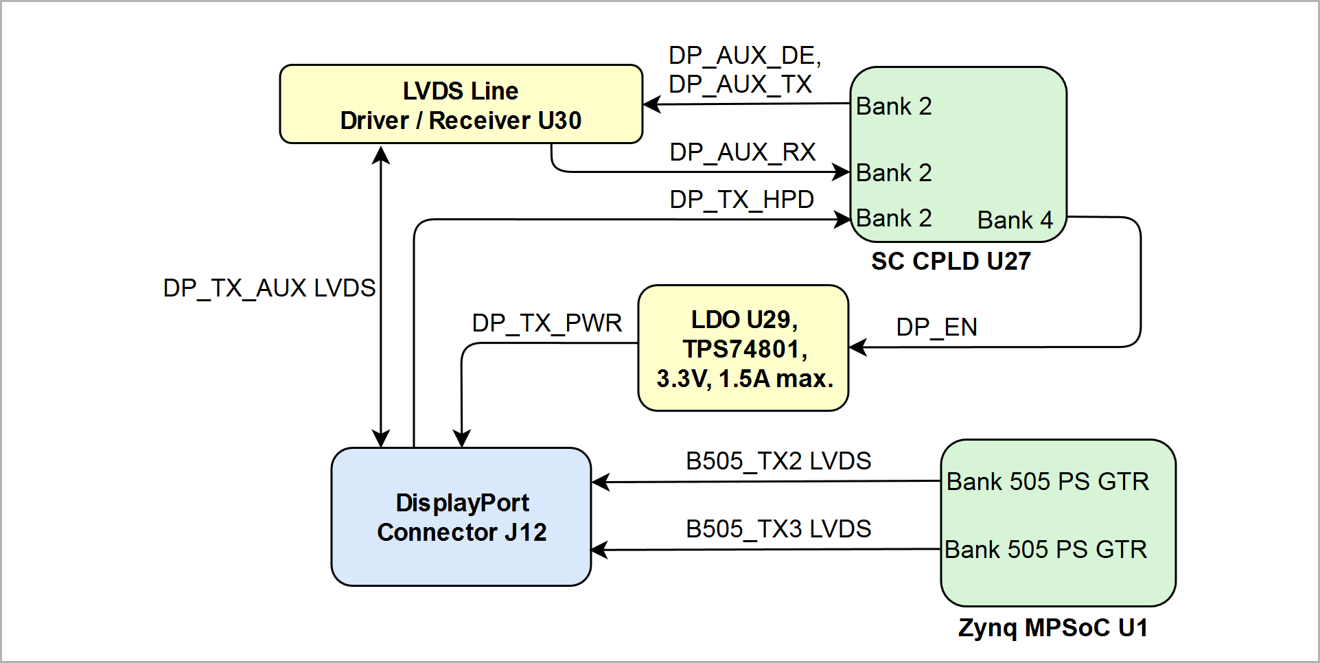
Follwowing table contains a brief description of the MGT lanes and control and status signals of the DisplayPort interface:
...
| Scroll Title | |||||||||||||||||||||||||||||||||||
|---|---|---|---|---|---|---|---|---|---|---|---|---|---|---|---|---|---|---|---|---|---|---|---|---|---|---|---|---|---|---|---|---|---|---|---|
| |||||||||||||||||||||||||||||||||||
|
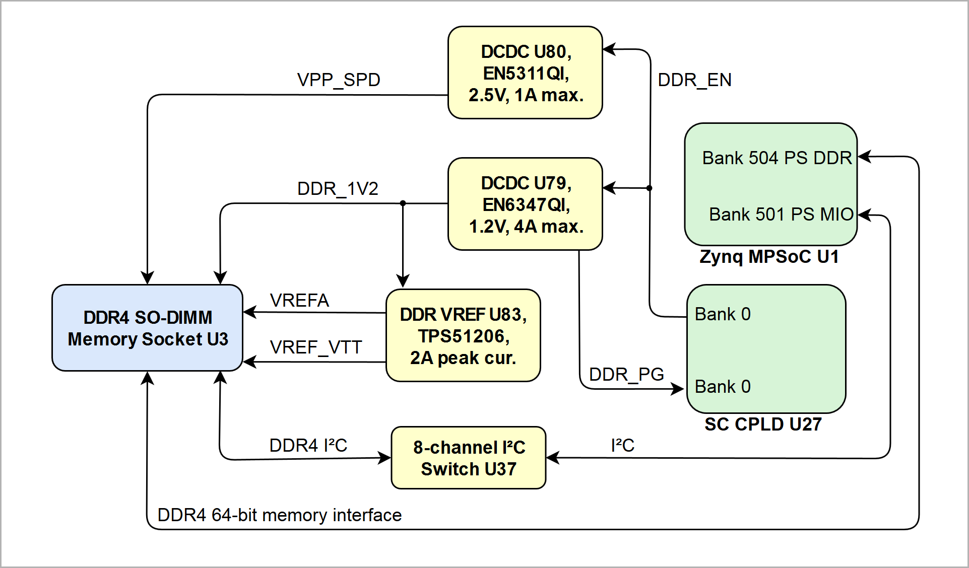
Following table gives an overview about the I/O signals of the DDR4 SDRAM memory interface:
| Connector | DDR4 SDRAM I/O Signal | Signal Schematic Name | Connected to | Notes |
|---|---|---|---|---|
DDR4 SO-DIMM Socket U13 | Address inputs |
| PS DDR Bank 504 | - |
| Bank address inputs |
| - | ||
| Bank group inputs |
| - | ||
| Differential clocks |
| 2 x DDR4 clock | ||
| Data input/output |
| - | ||
| Check bit input/output |
| - | ||
| Data strobe (differential) |
| - | ||
| Data mask and data bus inversion |
| - | ||
| Serial address inputs |
| address range configuration on I²C bus | ||
| Control Signals |
| chip selest signal | ||
| On-die termination enable | |||
| nRESET | |||
| Command and address parity input | |||
| Clock enable | |||
| CRC error flag | |||
| Activation command input | |||
| Temperature event | |||
| I²C |
| 8-channel I²C switch U37 | - |
Table 40: DDR4 64-bit memory interface signals and pins
Refer to the Xilinx Zynq UltraScale+ datasheet DS925 for more information on whether the specific package of the Zynq UltraScale+ MPSoC supports the maximum data transmission rate of 2400 MByte/s, which also depends on the used SO-DIMM module.
...
| Scroll Title | |||||||||||||||||||||||||||||||||
|---|---|---|---|---|---|---|---|---|---|---|---|---|---|---|---|---|---|---|---|---|---|---|---|---|---|---|---|---|---|---|---|---|---|
| |||||||||||||||||||||||||||||||||
|
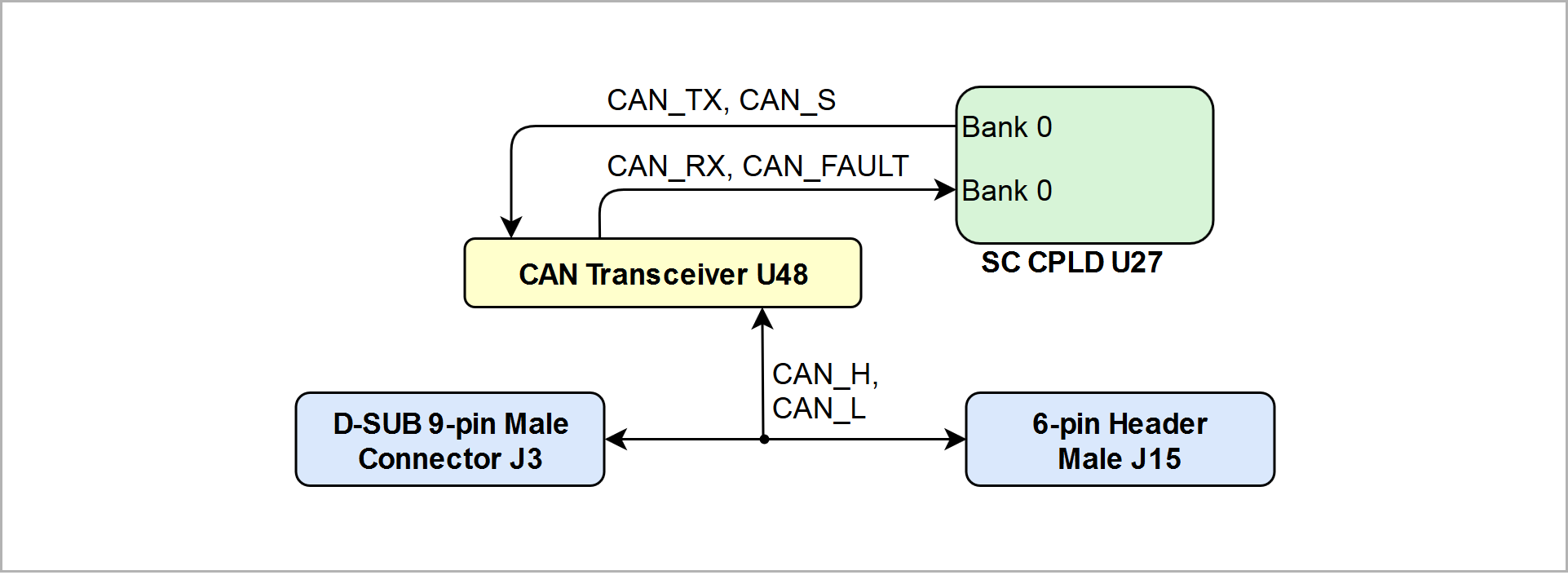
The CAN interface of external devices can be connected via D-SUB 9-pin male connector J3 or to the 6-pin male header J15:
| Connector | Signal Schematic Name | Connected to | Notes |
|---|---|---|---|
D-SUB 9-pin J3 |
| CAN Transceiver U48, pin 7 | - |
| CAN Transceiver U48, pin 6 | - | |
6-pin male header J15 |
| CAN Transceiver U48, pin 7 | - |
| CAN Transceiver U48, pin 6 | - | |
| CAN Transceiver | Signal Schematic Name | Connected to | Notes |
| TCAN337 U48 |
| SC CPLD U27, bank 0, pin C16 | 3.3V VCCIO |
| SC CPLD U27, bank 0, pin B15 | 3.3V VCCIO | |
| SC CPLD U27, bank 0, pin C15 | 3.3V VCCIO | |
| SC CPLD U27, bank 0, pin D15 | 3.3V VCCIO |
Table 41: CAN interface signals and pins
SD Card Interface
The SD Card interface of the TEB0911 board is routed via SD IO interface to the PS MIO bank 501 of the Zynq Ultrascale+ MPSoC (3.3V VCCO). The SC CPLD U27 controls the load switch Q3 to enable the card sockets J11 with signal 'SD_EN', bank 2, pin U11. The "Card Detect" and "Write Protect" signal are also routed to the SC CPLD:
| Scroll Title | ||||||||||||||||||||||||||||||||
|---|---|---|---|---|---|---|---|---|---|---|---|---|---|---|---|---|---|---|---|---|---|---|---|---|---|---|---|---|---|---|---|---|
| ||||||||||||||||||||||||||||||||
|
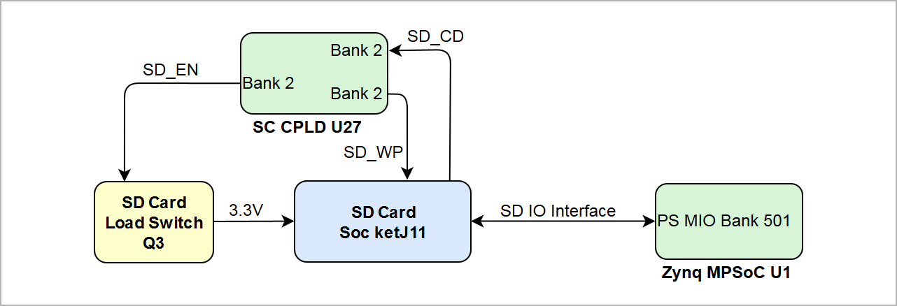
The SD Card socket have following signal and pin assignment:
| Connector | Signal Schematic Name | Connected to | Notes |
|---|---|---|---|
SD Card Socket J11 |
| PS bank 501 Pins: MIO46 ... MIO51 | - |
| - | ||
| - | ||
| - | ||
| - | ||
| - | ||
| SC CPLD U27, bank 2, pin T11 | Card Detect | |
| SC CPLD U27, bank 2, pin T10 | Write Protect |
...
| Scroll Title | |||||||||||||||||||||||||||||||||
|---|---|---|---|---|---|---|---|---|---|---|---|---|---|---|---|---|---|---|---|---|---|---|---|---|---|---|---|---|---|---|---|---|---|
| |||||||||||||||||||||||||||||||||
|
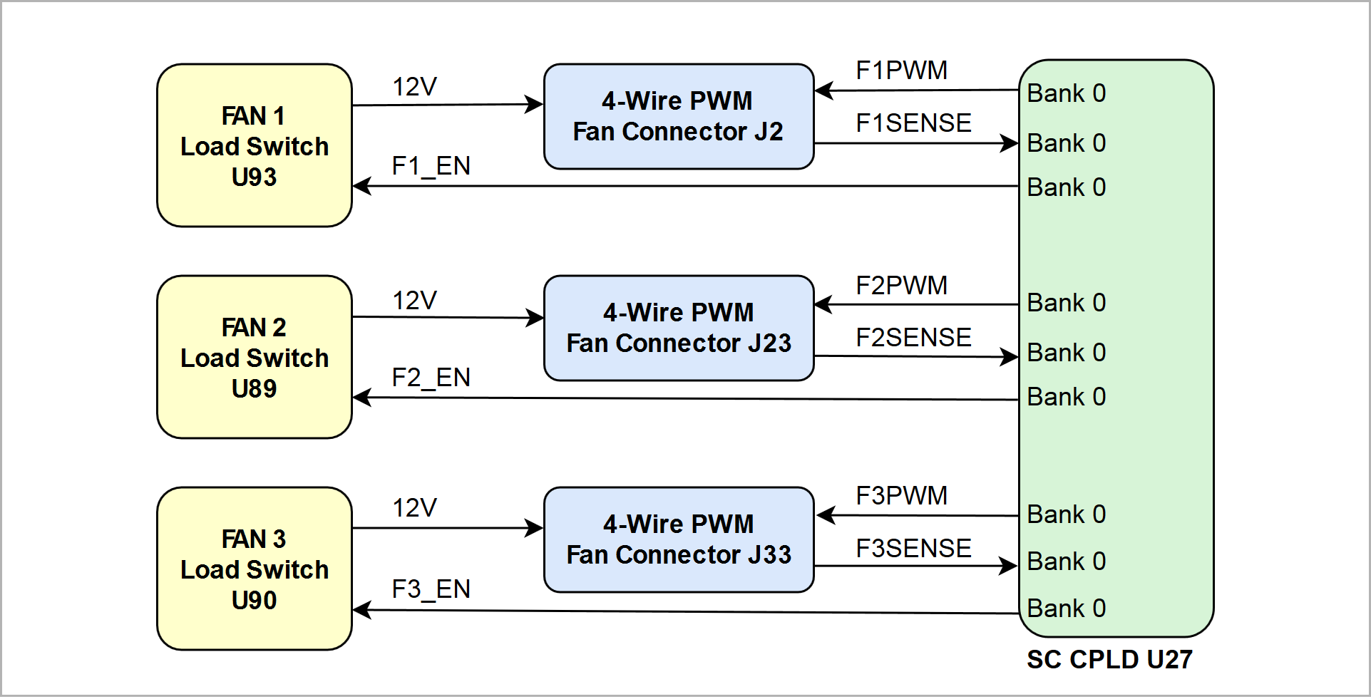
Following table contains a brief description of the control signals of the fan connectors:
| Connector | Signal Schematic Name | Connected to | Notes | |
|---|---|---|---|---|
Fan Connector J2 |
| SC CPLD U27, bank 0, pin E10 | -PWM signal to fan | |
| SC CPLD U27, bank 0, pin D11 | -sense RPM signal of fan | ||
| SC CPLD U27, bank 0, pin C8 | Controls 12V Load Switchenable 12V fan supply voltage | ||
Fan Connector J23 |
| SC CPLD U27, bank 0, pin D9 | -PWM signal to fan | |
| SC CPLD U27, bank 0, pin G12 | -sense RPM signal of fan | ||
| SC CPLD U27, bank 0, pin B4 | Controls 12V Load Switchenable 12V fan supply voltage | ||
Fan Connector J33 |
| SC CPLD U27, bank 0, pin B13 | -PWM signal to fan | |
| SC CPLD U27, bank 0, pin A13 | - | sense RPM signal of fan | |
| SC CPLD U27, bank 0, pin A12 | Controls 12V Load Switchenable 12V fan supply voltage |
Table 43: 4-wire PWM fan connectors signals and pins
...
| Scroll Title | |||||||||||||||||||||||||||||||||
|---|---|---|---|---|---|---|---|---|---|---|---|---|---|---|---|---|---|---|---|---|---|---|---|---|---|---|---|---|---|---|---|---|---|
| |||||||||||||||||||||||||||||||||
|
| Connector | Signal Schematic Name | Connected to | Notes |
|---|---|---|---|
Pin Header J22 |
| clock generator U17, pin 16 | PS_1V8 VCCIO |
| clock generator U17, pin 18 | ||
SMA Coax J25 |
| clock generator U17, pin 1 | - |
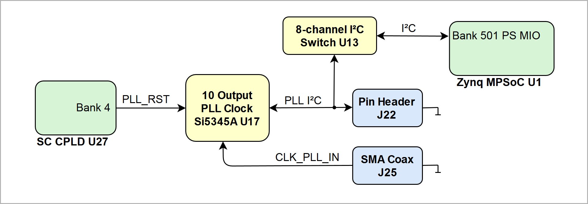
Table 44: Clock generator Si5345A external interfaces
On-board Peripherals
| HTML |
|---|
<!-- Components on the Module, like Flash, PLL, PHY... --> |
...
| Scroll Title | |||||||||||||||||||||||||||||||||
|---|---|---|---|---|---|---|---|---|---|---|---|---|---|---|---|---|---|---|---|---|---|---|---|---|---|---|---|---|---|---|---|---|---|
| |||||||||||||||||||||||||||||||||
|
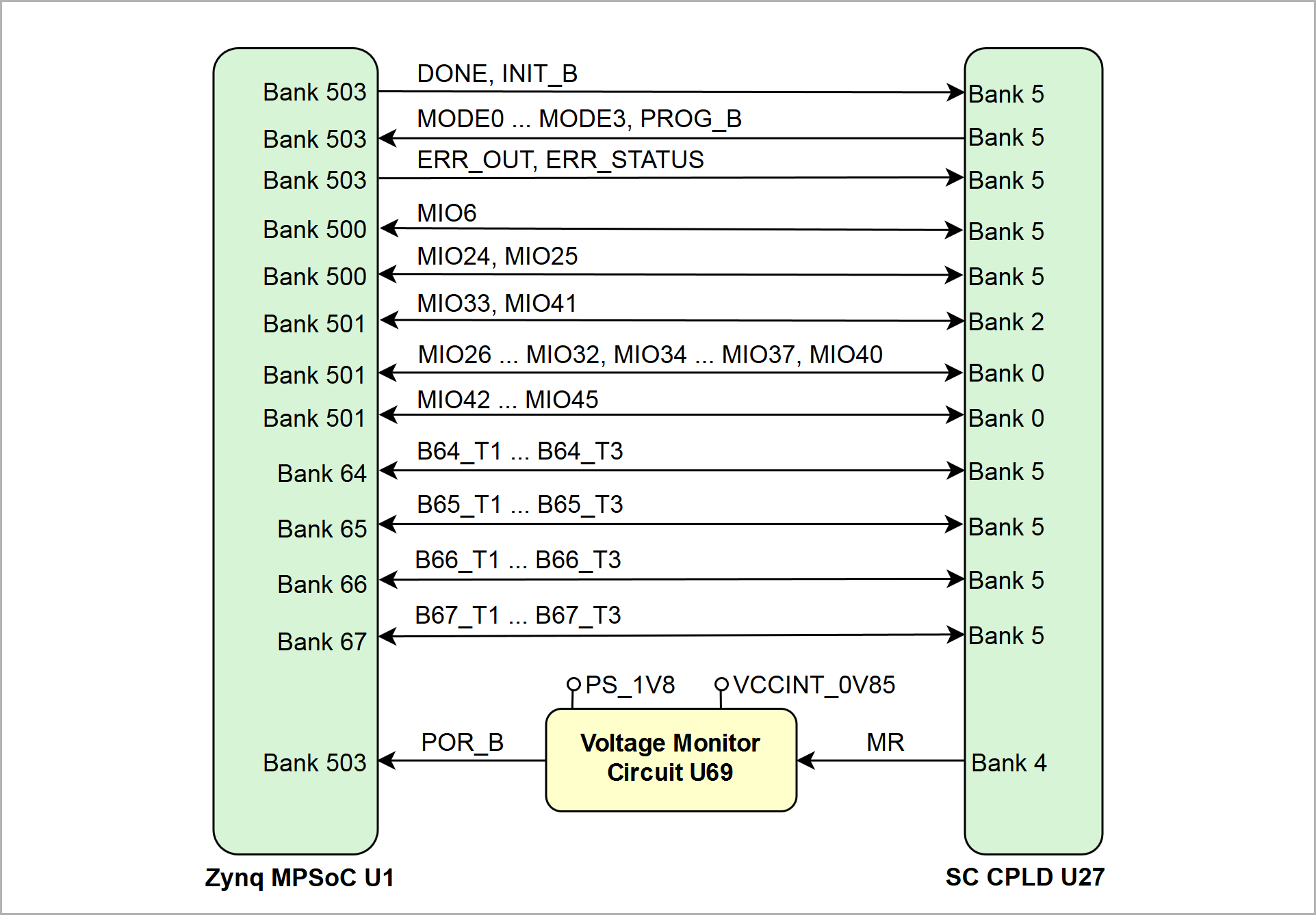
For detailed information about the current function of the MIO-pin in conjunction with the SC CPLD, the internal signal assignment and implemented logic, refer to the Wiki reference page of the SC CPLD firmware of this board or into the bitstream file of the SC CPLD.
...
Table 46: MIO-pin assignment of the module's I2C interface
| Info |
|---|
| The I²C switches can be reseted simultanously by the pin 'I2C_RST', which is connected to SC CPLD U27, bank 4 pin L2 with low active logic. |
I2C addresses (7 bit without read/write-bit) for on-board slave devices are listed in the table below:
...
The TEB0911 carrier board contains several EEPROMs for configuration and general user purposes. The EEPROMs are provided by Microchip and all have , the I²C interfaces of the EEPROM's are multiplexed to the I²C switch U37:
| EEPROM Modell | Designator | Memory Density | Purpose |
|---|---|---|---|
| 24LC128-I/ST | U57 | 128 Kbit | user |
| 24AA025E48T-I/OT | U60 | 2 Kbit | user |
| 24AA025E48T-I/OT | U45 | 2 Kbit | user |
| 24AA025E48T-I/OT | U83 | 2 Kbit | user |
| 24LC128-I/ST | U5 | 128 Kbit | USB3 Hub U4 configuration memory |
...
| Clock Source | Signal Schematic Name | Frequency | Clock Input Destination |
|---|---|---|---|
| SiTime SiT8008BI oscillator, U22 |
| 33.333333 MHz | Zynq MPSoC PS Config Bank 503, pin U24 |
| SiTime SiT8008AI oscillator, U16 |
| 52.000000 MHz | USB2 transceiver PHY U15, pin 26 |
| Kyocera CX3225SB26000, Y3 | - | 26.000 MHz | 4-port USB3 Hub U4, pin 68/69 |
| Kyocera CX3225SB26000, Y2 |
| 54.000 MHz | PLL clock generator U17, pin 8/9 |
| SiTime SiT8008BI oscillator, U21 |
| 25.000000 MHz | Gigabit Ethernet PHY U20, pin 34 |
SiTime SiT8008AI oscillator, U87 optional, not equipped |
| 25.000000 MHz | System Controller CPLD U27, bank 2, pin AA9 |
| SiTime SiT8008BI oscillator, U18 |
| 25.000000 MHz | PLL clock generator U17, pin 63 |
| SiTime SiT8008AI oscillator, U85 | - | 25.000000 MHz | PLL clock generator U12, pin 3 |
DSC1123 oscillator, U92 optional, not equipped |
| 100.0000 MHz | PS GTR Bank 505 Lane 3, dedicated for DisplayPort, Pin pin U31, U32 |
Table 50: Reference clock signal oscillators
...
| Si5338A Pin | Signal Schematic Name | Connected to | Clock Direction | Note |
|---|---|---|---|---|
IN1 |
| U17, pin 54 | Input | Differential reference clock input from PLL clock generator U17 |
| IN2 |
| U17, pin 53 | Input | |
IN3 | - | U85, pin 3 | Input | 25.000000 MHz oscillator, Si8008AI |
IN4 | - | GND | Input | LSB (pin 'IN4') of the default I²C-adress 0x70 not set |
IN5 | - | Not connected | Input | Not used |
| IN6 | - | GND | Input | Not used |
CLK0A |
| U2, pin 55 | Output | NGFF M.2 PCIe socket (Key M), |
| CLK0B |
| U2, pin 53 | Output | |
| CLK1A |
| U1, pin U27 | Output | PS GTR Bank 505 Lane 2, dedicated for DisplayPort, |
| CLK1B |
| U1, pin U28 | Output | |
| CLK2A |
| U1, pin W27 | Output | PS GTR Bank 505 Lane 1, dedicated for USB3 interface |
| CLK2B |
| U1, pin W28 | Output | |
| CLK3A |
| U1, pin AA27 | Output | PS GTR Bank 505 Lane 0, dedicated for SSD interface |
| CLK3B |
| U1, pin AA28 | Output |
...
| LED | Color | Connected to | Description and Notes |
|---|---|---|---|
| D6 | red | Zynq MPSoC U1, pin W21 | Reflects inverted DONE signal. ON when FPGA is not configured, |
| D17 | green | USB3 Hub U4, pin 25 | LED is on if all USB3 and USB2 ports are in the suspend state and is |
| D18 | green | USB3 Hub U4, pin 4 | LED output for downstream 1 port. |
| D19 | green | USB3 Hub U4, pin 63 | LED output for downstream 3 port. |
| D2 | red | SC CPLD U27, bank 2, pin AB17 | SFP+ interface status. The LEDs are fitted on-board under the SFP+ connector cage. |
| D4 | green | SC CPLD U27, bank 2, pin AB18SFP+ interface status LED | |
| D3 | red | SC CPLD U27, bank 2, pin AA16 | SFP+ interface status LED |
| D5 | green | SC CPLD U27, bank 2, pin AB15 | SFP+ interface status LED |
| D13 | green | SC CPLD U27, bank 2, pin U12 | functionality depends on the current firmware of the SC CPLD U27 refer to the documentation section: LED |
| D14 | green | SC CPLD U27, bank 2, pin V12 | |
| D15 | green | SC CPLD U27, bank 2, pin W12 | |
| D16 | red | SC CPLD U27, bank 2, pin V13 |
...
| Scroll Title | ||||||||||||||||||||||||
|---|---|---|---|---|---|---|---|---|---|---|---|---|---|---|---|---|---|---|---|---|---|---|---|---|
| ||||||||||||||||||||||||
| ||||||||||||||||||||||||
| revision | 11 |
|
| Scroll Only |
|---|
|
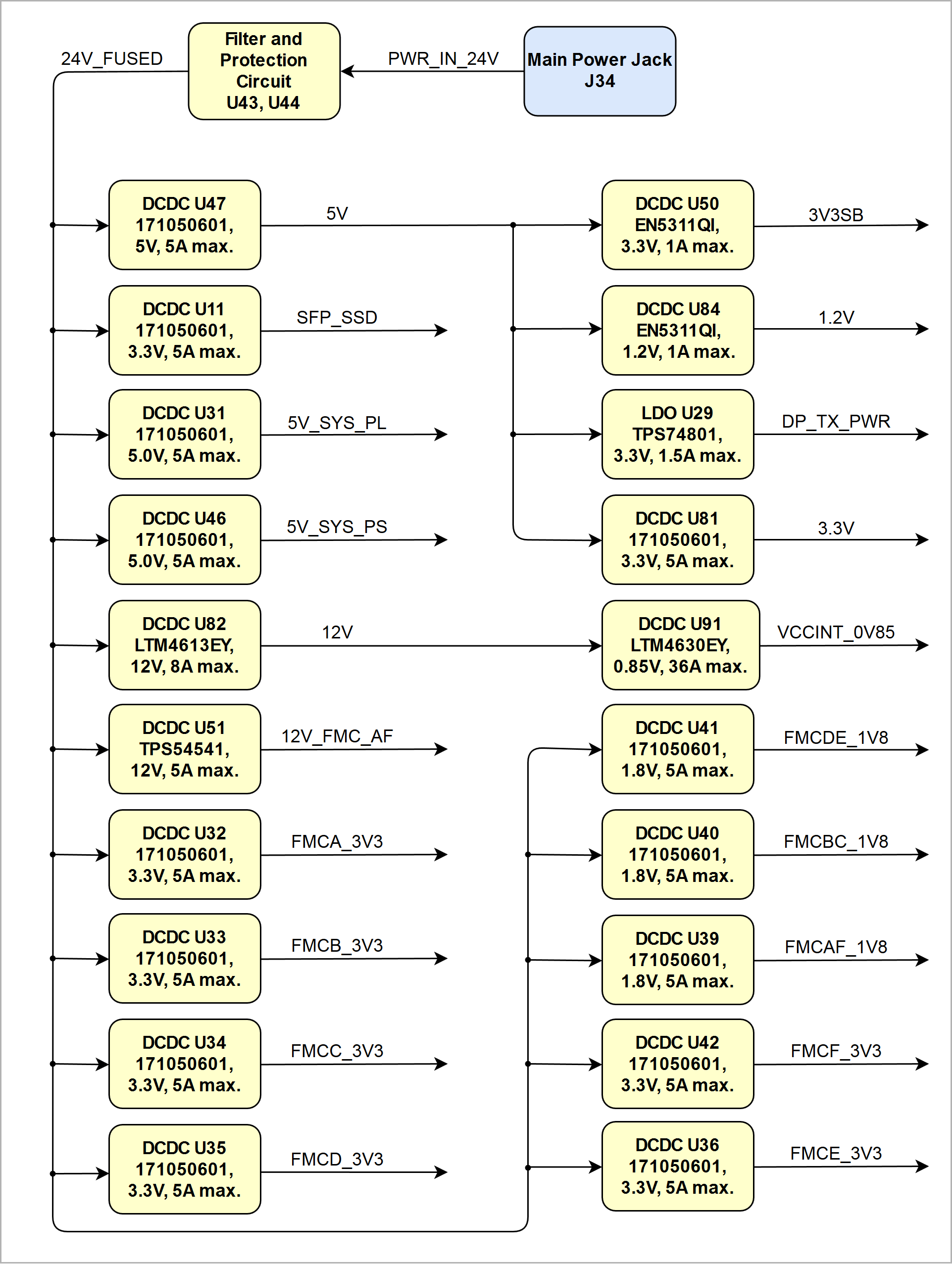
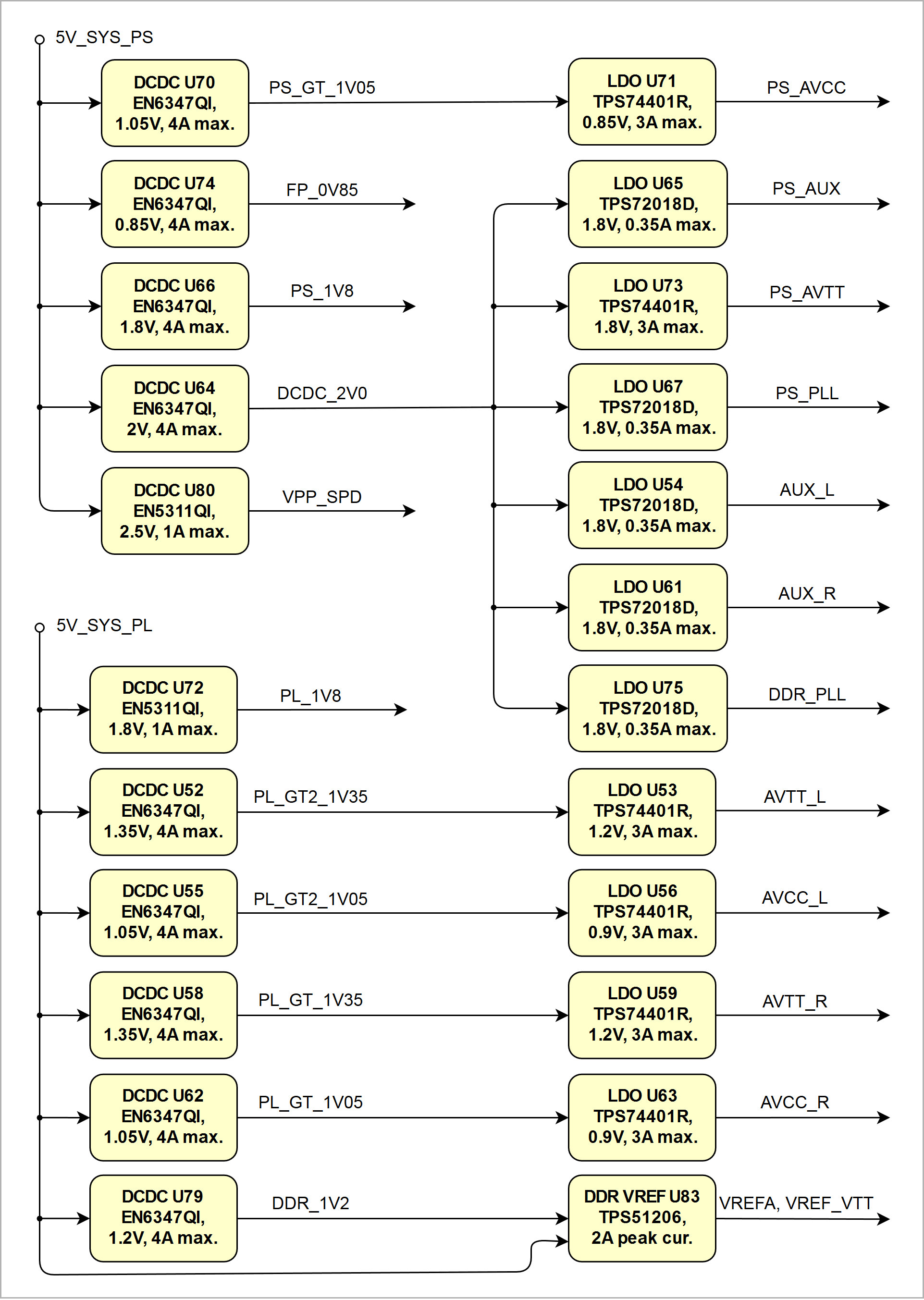
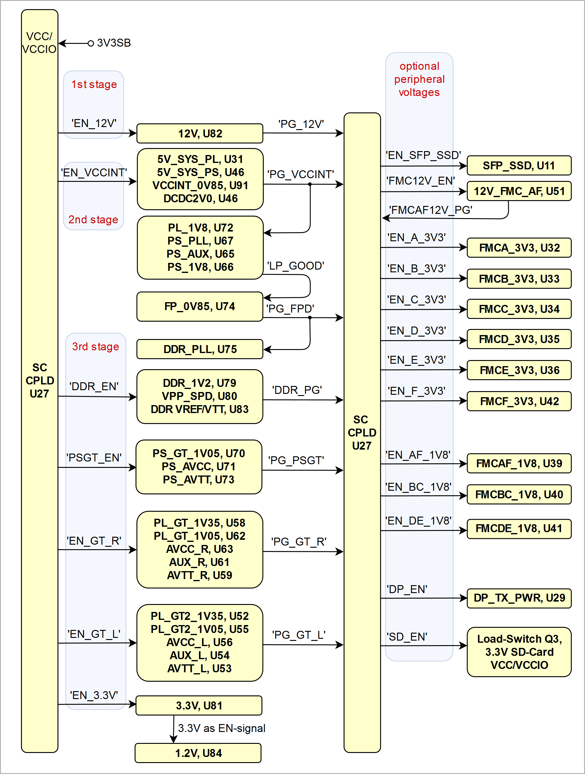
Power distribution to the MPSoC PS and PL units:
| Scroll Title | ||||||||||||||||||||||||||||||
|---|---|---|---|---|---|---|---|---|---|---|---|---|---|---|---|---|---|---|---|---|---|---|---|---|---|---|---|---|---|---|
| ||||||||||||||||||||||||||||||
| ||||||||||||||||||||||||||||||
| Warning | ||||||||||||||||||||||||||||||
|
| Info |
|---|
Note: The DC-DC converter U91 LTM4630EY has an integrated temperature diode for device temperature monitoring. The analog signal 'TEMP_CORE_DC' on pin J6 of the converter is routed to the dedicated differential analog interface (XADC) of the Zynq MPSoC, pin U18 (V_P), pin V17 (V_N) is connected to analog GND_N) is connected to analog GND. |
| Warning |
|---|
| To avoid any damage to the module, check for stabilized on-board voltages should be carried out(i.e. power good and enable signals) before powering up any SoC's I/O bank voltages VCCO_x. All I/Os should be tri-stated during power-on sequence. |
Power-On Sequence
The TEB0911 UltraRack board meets the recommended criteria to power up the Xilinx Zynq UltraScale+ MPSoC properly by keeping a specific sequence of enabling the on-board DC-DC converters dedicated to the particular Power Domains and powering up the on-board voltages.
...
| Scroll Title | ||||||||||||||||||||||||||||||||
|---|---|---|---|---|---|---|---|---|---|---|---|---|---|---|---|---|---|---|---|---|---|---|---|---|---|---|---|---|---|---|---|---|
| ||||||||||||||||||||||||||||||||
|
Power Rails
| Peripheral Designator | VCC / VCCIO Schematic Name | Voltage | Direction | Pins | Notes |
|---|---|---|---|---|---|
| J12 | DP_TX_PWR | 3.3V | Out | Pin 20 | Display-Port Connector |
| J9A | SFP_SSD | 3.3V | Out | Pin T15, T16 | SFP+ 2x1 Connector |
| J9B | SFP_SSD | 3.3V | Out | Pin L15, L16 | |
| J13A | VBUS1 | 5.0V | Out | Pin U1 | USB3 Ports |
| J13B | VBUS2 | 5.0V | Out | Pin U10 | |
| J11 | - | 3.3V | Out | Pin 4 | MicroSD Card Socket |
| B1 | PSBATT | 3.0V | In | Pin + | Battery Holder CR1220 |
| U2 | SSD1_3V3_1 | 3.3V | Out | Pin 2, 4 | SSD PCIe connector |
| SSD1_3V3_2 | 3.3V | Out | Pin 70, 72, 74 | ||
| SSD1_3V3_3 | 3.3V | Out | Pin 12, 14, 16, 18 | ||
| U3 | DDR_1V2 | 1.2V | Out | Pin 111, 112, 117, 118, 123, 124, 129, 130, 135, 136, 141, 142, 147, 148, 153, 154, 159, 160, 163 | DDR4 SO-DIMM socket |
| VPP_SPD | 2.5V | Out | Pin 255, 257, 259 |
Table 57: Power pin description of Peripheralsperipherals' Connectorconnectors
| XMOD / JTAG Designator | VCC / VCCIO Schematic Name | Voltage | Direction | Pins | Notes |
|---|---|---|---|---|---|
| J24 | 3V3SB | 3.3V | Out | Pin 5 | Zynq MPSoC JTAG |
| PS_1V8 | 1.8V | Out | Pin 6 | ||
| J35 | 3V3SB | 3.3V | Out | Pin 5, 6 | SC CPLD JTAG |
...
| Parameter | Min | Max | Units | Reference Document | Notes | |||||
|---|---|---|---|---|---|---|---|---|---|---|
| VIN supply voltage | 22 | 25 | V | Schematic REV03 | 24V nominal | |||||
| VBATT | 2.2 | 5.5 | V | TPS780180300 data sheet | supplied by 3.0V CR1220 battery | |||||
| PL I/O input voltage (HP / HD bank) | -0.2 | VCCO + 0.2 | V | Xilinx DS925 data sheet | PL bank VCCO voltages are fixed at 1.8V | |||||
| PS I/O input voltage | -0.2 | VCCO + 0.2 | V | Xilinx DS925 data sheet | see section 'bank voltages' for PS bank VCCO | |||||
| SC CPLD U27 I/O input voltage | -0.3 | 3.6 | V | Lattice MachXO2 familiy data sheet | - | |||||
| SC CPLD U27 differential I/O input voltage | 0 | 2.605 | V | Lattice MachXO2 familiy data sheet | - | PLL clock generator input | -0.23.0 | V | Si5345/44/42 Rev D Data Sheet | - |
| Operating temperature | 0 | 60 | °C | F455B / Xilinx DS925 data sheet | - |
...
Operating Temperature Ranges
The TEB0911 board is capable to be operated at an operational temperatur range of operational temperature range is 0 °C ... 85 °C without FMC cooling fans M1 ... M6 and NGFF M.2 PCIe socket U2, which limit the temperatur range.
Physical Dimensions
Module Board size: ... mm 406mm × 234... mm30mm. Please download the assembly diagram for exact numbers.
Mating height with standard connectors: ... mm.
PCB thickness: 1... 65 mm.
Highest part on PCB: approx. ... mm. Please download the step model for exact numbers.
...
| Scroll Title | ||||
|---|---|---|---|---|
| ||||
|
| Scroll Title | ||||
|---|---|---|---|---|
| ||||
|
Revision History
Hardware Revision History
| Date | Revision | Notes | Link to PCN | Documentation Link |
|---|---|---|---|---|
| - | 03 | current Current available board revision | - | TEB0911-03 |
| - | 02 | First Second production release | - | TEB0911-02 |
| - | 01 | PrototypesFirst production release | - | TEB0911-01 |
Table 65: Module hardware revision history
Hardware revision number can be found on the PCB board together with the board model number separated by the dash.
...
| HTML |
|---|
<!-- Generate new entry: 1.add new row below first 2.Copy "Page Information Macro(date)" Macro-Preview, Metadata Version number, Author Name and description to the empty row. Important Revision number must be the same as the Wiki document revision number 3.Update Metadata = "Page Information Macro (current-version)" Preview+1 and add Author and change description. --> |
Date | Revision | Contributors | Description | ||||||||||||||||||||||||||
|---|---|---|---|---|---|---|---|---|---|---|---|---|---|---|---|---|---|---|---|---|---|---|---|---|---|---|---|---|---|
|
|
|
| ||||||||||||||||||||||||||
| 2019-08-27 | v.184 | John Hartfiel |
| ||||||||||||||||||||||||||
| 2019-05-10 | v.183 | John Hartfiel |
| ||||||||||||||||||||||||||
| 2018-07-23 | v.182 | Ali Naseri |
| ||||||||||||||||||||||||||
| -- | all |
|
Table 66: Document change history
...
Overview
Content Tools