Page History
| HTML |
|---|
<!--
Template Revision 1.6
(HTML comments will be not displayed in the document, no need to remove them. For Template/Skeleton changes, increase Template Revision number. So we can check faster, if the TRM style is up to date).
--> |
| Scroll Ignore |
|---|
| Scroll pdf ignore | |
|---|---|
Table of Contents
|
Overview
...
Download PDF Version of this Document.
| Scroll pdf ignore | ||||
|---|---|---|---|---|
Table of Contents
|
Overview
| Scroll Only (inline) |
|---|
Online version of this manual and other related documents can be found at https://wiki.trenz-electronic.de/display/PD/TE0741
|
The TE0741 module is available in four different logic densities (70T, 160T, 325T and 410T). The 70T and 160T devices can be programmed with the free Xilinx Vivado WebPACK software. Further information about the Kintex-7 FPGA can be found in the Xilinx document 7 Series FPGA's Overview (DS180).
Block Diagram
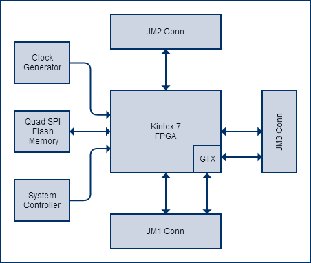
Figure 1: TE0741 Block Diagram.
Main Components
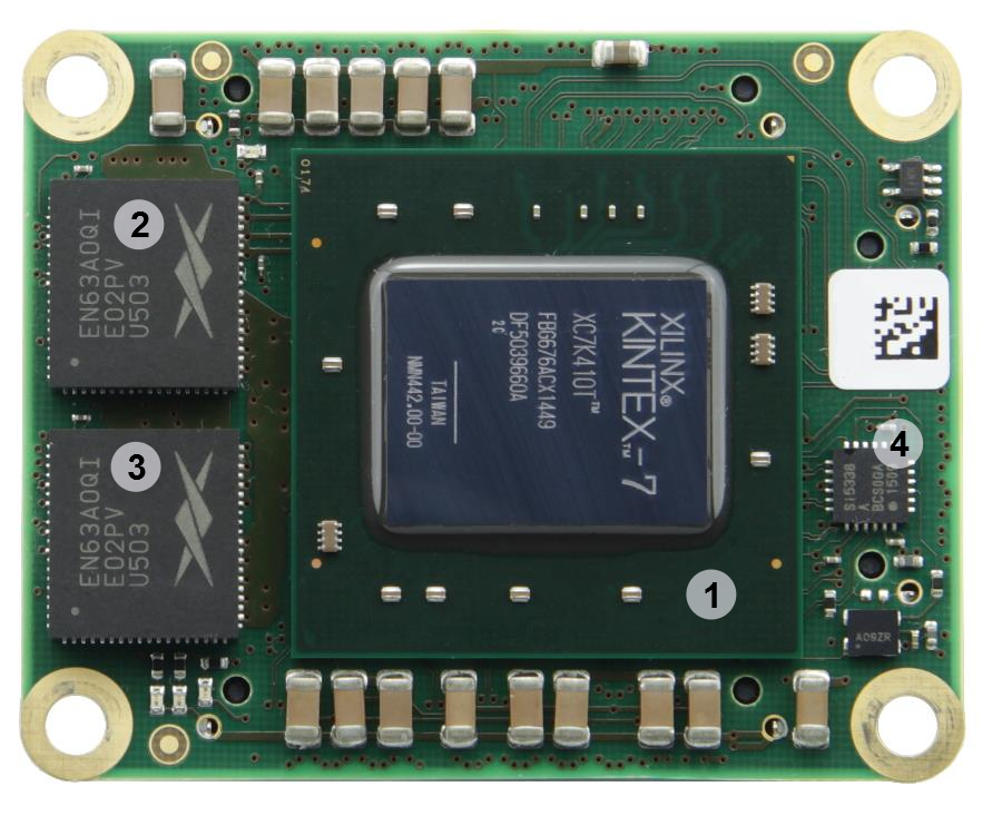
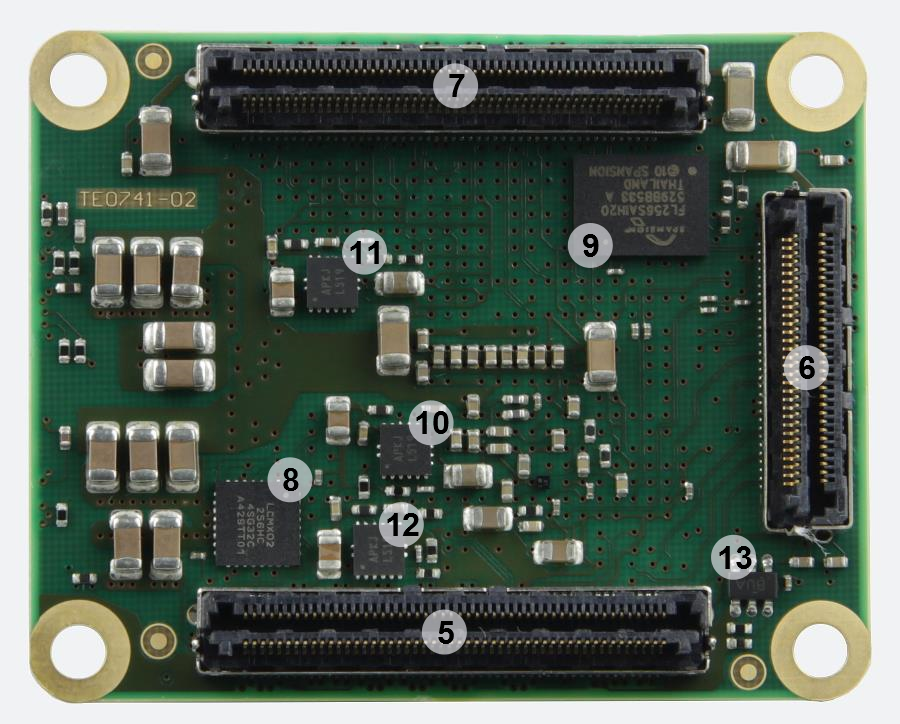
Figure 2: TE0741 (REV 02).
| Scroll Only (inline) |
|---|
Refer to http://trenz.org/te0741-info for online version of this manual and the rest of available documentation. |
Key Features
- Industrial-grade Xilinx Kintex-7 FPGA
...
- module (70T*, 160T*, 325T, 410T)
* Devices supported by the free Xilinx Vivado WebPACK software. - 256-Mbit (32-MByte) Quad SPI Flash memory (for configuration and operation) accessible through:
- FPGA
- JTAG port (SPI indirect (Bus width x4))
- 8 GTX transceivers
- FPGA configuration through:
- JTAG (B2B connector)
- SPI Flash memory
- 25 MHz low jitter oscillator with shutdown control
- Programmable quad PLL clock generator
- On-board high-efficiency DC-DC converters
- GTX voltage regulators with control enable
- Core voltage regulator: 20A (2 x Enpirion DC-DC regulators with load-sharing)
- Supply voltages: either 3.3V or 3.3V and 5V
- Plug-on module with two 100-pin and one 60-pin high-speed hermaphroditic stacking strips
- Up to 144 (94 for 70T) FPGA I/O pins are available on B2B strips (up to 65 LVDS pairs possible)
- 2 user LED's, 1x DONE FPGA pin LED, 1 System Controller status LED
- System management and power sequencing
- AES bit-stream encryption
- eFUSE bit-stream encryption
- Evenly spread supply pins for good signal integrity
Additional assembly options are available for cost or performance optimization upon request.
| Page break |
|---|
Block Diagram
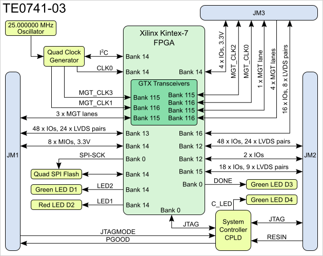
Figure 1: TE0741 block diagram.
| Page break |
|---|
Main Components
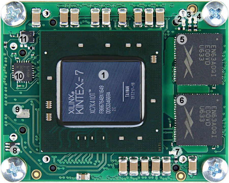
Figure 2.1: TE0741--03-410-2CF module.

Figure 2.2: TE0741-03-160-2C1 module.
- Xilinx Kintex-7 FPGA, U1
- Green LED (DONE), D3
- Red LED (LED1), D2
- Green LED (LED2), D1
- EN63A0QI Voltage Regulator 1.0V (Master), U14
- EN63A0QI Voltage Regulator 1.0V (Slave), U15
- Green LED (C_LED), D4
Voltage detector, U11
- Serial number (traceability) pad
- I2C-programmable any-frequency, any-output quad clock generator, U2
- Low-power programmable oscillator @ 25.000000 MHz, U3
- Samtec Razor Beam™ LSHM-150 B2B connector, JM2
- 32 MByte quad SPI Flash memory, U4
- Samtec Razor Beam™ LSHM-130 B2B connector, JM3
- 3A PFET load switch with configurable slew rate (3.3V), Q1
- Samtec Razor Beam™ LSHM-150 B2B connector, JM1
- System Controller CPLD, U7
- EP53F8QI Voltage Regulator (1.2V_MGT), U6
- EP53F8QI Voltage Regulator (1.8V), U8
- EP53F8QI Voltage Regulator (1V_MGT), U16
Key Features
- Industrial-grade Xilinx Kintex-7 FPGA module (70T*, 160T*, 325T, 410T)
* Device supported by the free Xilinx Vivado WebPACK software. - 256 Mbit (32 MByte) Quad SPI Flash memory (for configuration and operation) accessible through:
- FPGA
- JTAG port (SPI indirect (Bus Width x4))
- 8 GTX transceivers
- FPGA configuration through:
- JTAG (B2B connector)
- SPI Flash memory
- 25 MHz low jitter oscillator with shutdown control
- Programmable quad PLL-clock generator
- On-board high-efficiency DC-DC converters
- GTX voltage regulators with control enable
- Core voltage regulator: 20A (2 x Enpirion DC/DC regulators with load-sharing)
- Supply voltages: either 3.3V or 3.3V and 5V
- Plug-on module with two 100-pin and one 60-pin high-speed hermaphroditic stacking strips
- Up to 144 (94 for 70T) FPGA I/O pins available on B2B strips (up to 65 LVDS pairs possible)
- 2 user LED's, 1 DONE FPGA pin LED, 1 System Controller status LED
- System management and power sequencing
- AES bit-stream encryption
- eFUSE bit-stream encryption
- Evenly spread supply pins for good signal integrity
- Assembly options for cost or performance optimization available on request
...
Initial Delivery State
| Storage device name | Content | Notes |
|---|---|---|
SPI Flash OTP Area | Empty, not programmed | Except serial number programmed by flash vendor. |
Programmed | - | |
SPI Flash main array | Demo design | - |
EFUSE USER | Not programmed | - |
EFUSE Security | Not programmed | - |
Table 1: Initial delivery state.
Signals, Interfaces and Pins
Board to Board (B2B) I/Os
I/O signals connected to the FPGA's I/O banks and B2B connector:
SPI Flash OTP Area | Empty, not programmed | Except serial number programmed by flash vendor. |
SPI Flash Quad Enable bit | Programmed | - |
SPI Flash main array | Demo design | - |
eFUSE USER | Not programmed | - |
eFUSE Security | Not programmed | - |
Table 1: Initial delivery state.
Signals, Interfaces and Pins
Board to Board (B2B) I/Os
Overview of the I/O signal banks connected to the B2B connectors:
| Bank | Type | B2B Connector | I/O Signal Count | Voltage | Notes |
|---|---|---|---|---|---|
0 | HR | - | - | 3.3V | Configuration bank. |
12 | HR | JM2 | 50 I/Os, 24 LVDS pairs | User | Supported voltage level |
0
HR
-
-
12
HR
JM2
50 I/O-pins
24 LVDS-pairs possible
User
HR-Banks support voltages from 1.2V to 3.3V standards.
NOTE: BANK 12 IS NOT AVAILABLE ON THE K70T DEVICE.
13
HR
JM1
48 I/O-pins
24 LVDS-pairs possible
User
14
HR
JM1,
JM3
8 I/O-pins,
4 I/O-pins (2 LVDS-pairs possible)
3.3V
15
HR
JM2
18 I/O-pins
9 LVDS-pairs possible
User
from 1.2V to 3.3V |
. NOTE: BANK 12 IS NOT AVAILABLE ON THE K70T DEVICE! | ||
13 | HR | JM1 |
48 I/ |
Os, 24 LVDS pairs | User |
| Supported voltage level from 1.2V to 3.3V |
| . |
14 |
HR |
JM1 |
NC
-
-
33
HP
NC
-
-
Table 2: Voltage ranges and pin-outs of available logic banks of the FPGA.
Please use Master Pin-out Table table as primary reference for the pin mapping information.
JTAG Interface
JTAG access to the Xilinx Kintex7 and to the System Controller CPLD is provided through B2B connector JM2.
...
JM2-93
Table 3: Pin-mapping of JTAG Interface on B2B connector
| Note |
|---|
| Select by JTAGMODE pin on B2B connector JM1-89 either to access FPGA Artix7 (JTAGMODE pin driven low or open) or System Controller via JTAG (JTAGMODE pin driven high). |
System Controller I/O Pins
Special purpose pins are connected to smaller System Controller CPLD and have following default configuration:
...
JM3 | 8 I/Os 4 I/Os, 2 LVDS pairs | 3.3V | IO pins at B2B connector JM1, support only 3.3V. | ||
15 | HR | JM2 | 18 I/Os, 9 LVDS pairs | User | Supported voltage level from 1.2V to 3.3V. |
16 | HR | JM3 | 16 I/Os, 8 LVDS pairs | User | Supported voltage level from 1.2V to 3.3V. |
32 | HP | NC | - | - | Bank not used. |
33 | HP | NC | - | - | Bank not used. |
| 34 | HP | NC | - | - | Bank not used. |
Table 2: Available I/O signal banks connected to the B2B connectors.
Please use Master Pin-out Table table as primary reference for the pin mapping information.
JTAG Interface
JTAG access to the Xilinx Kintex-7 and to the System Controller CPLD is provided through B2B connector JM2.
| JTAG Signal | B2B Connector |
|---|---|
| TMS | JM2-93 |
| TDI | JM2-95 |
| TDO | JM2-97 |
| TCK | JM2-99 |
Table 3: Pin-mapping of JTAG Interface on B2B connector.
| Note |
|---|
| JTAGMODE pin 89 in B2B connector JM1 is used to select which device is accessible, low - Xilinx Kintex-7, high - System Controller CPLD. |
System Controller I/O Pins
Special purpose pins are connected to smaller System Controller CPLD and have following default configuration:
| Pin Name | Mode | Function | Default Configuration | B2B Connector |
|---|---|---|---|---|
| PGOOD | INOUT | Power Good | Active low when all on-module power supplies failed, otherwise high impedance | JM1-30 |
| RESIN | Input | Reset | Active low reset signal, drive low to keep the system in reset (FPGA pin PROG_B will be driven by CPLD). | JM2-18 |
| JTAGMODE | Input | JTAG Select | Low for normal operation, high (3.3V) to program the System Controller CPLD. | JM1-89 |
Table 4: Pin-description of System Controller CPLD. Important, functionality depends on CPLD Firmware, see TE0741 CPLD. General 4x5 module controller IO description on 4 x 5 SoM Integration Guide#4x5SoMIntegrationGuide-4x5ModuleControllerIOs
On-board LEDs
There are four LED's available on TE0741 SoM. Two status LED's (D3 and D4) and two user configurable LED's (D1 and D2).
| LED | Color | Connected to | Description and Notes |
|---|---|---|---|
| D1 | Green | LED2 | User configurable LED. |
| D2 | Red | LED1 | User configurable LED. |
| D3 | Green | DONE | Reflects inverted DONE signal, ON when FPGA is not configured, OFF as soon as PL is configured. This LED will not operate if the the 3.3V power rail is not available. After FPGA configuration the user can use USRACCESSE2 to control Done LED. |
| D4 | Green | C_LED | Connected to the system controller indicating status of the module, functionalitly, see: TE0741 CPLD#LED |
Table 4: Pin-description of System Controller CPLD
LED's
There are four LED's available on TE0741 SoM. Two status LED's (D3 and D4) and two user configurable LED's (D1 and D2).
Reflects inverted DONE signal, ON when FPGA is not configured, OFF as soon as PL is configured.
This LED will not operate if the the 3.3V power rail is not available.
After FPGA configuration the user can use USRACCESSE2 to control Done LED.
Connected to the system controller indicating status of the module:
Steadily lit: RESIN pin is kept low.
Blinking fast (0.1s on/off): Power sequencing fault (PG_ALL = 0).
Blinking at medium speed (0.5s on/off): Power sequencing has completed but the FPGA is not configured (PG_ALL = 1, DONE = 0).
Blinking slow (1s on/off): FPGA is configured and board is ready (PG_ALL = 1, DONE = 1).
It is also possible to program the System Controller CPLD to connect this LED to FPGA pin named XIO.Table 5: Description of the on board LED's.
Note: if FPGA logic toggles DONE pin (to control D3) then D4 will toggle at random, as changing value on DONE will change the blink frequency of D4.
| Note |
|---|
DONE LED will be ON as long as FPGA is NOT configured and will be OFF when FPGA is configured successfully. If user STARTUPE2 primitive is used in user design then DONE LED is controlled by the user design and can be on/off/blink or have any other functionality defined by the user. |
Clocking
To enable the PLL (phase-locked loop) clock generator Si5338A (U2), CLK_EN-signal (bank 14, pin C26) must be set to high, to activate the 25 MHz reference clock SiT8208AI (U3). The GTX reference clocks 0 and 2 have to be provided by the user on B2B connector JM3.
| Clock | Frequency | IC | FPGA | Notes |
|---|---|---|---|---|
PLL reference | 25 MHz | U3 SiT8208AI | - | Activated by CLK_EN pin of FPGA. |
GTX REFCLK0 | - | B2B | D5/D6 | B2B connector pins: MGT_CLK_0_N: JM3-31 MGT_CLK_0_P: JM3-33 Needs decoupling and differential terminator on base board. |
| GTX GTX REFCLK1 | 125 MHz | U2 Si5338 | F5/F6 | PLL clock 1, default frequency is 125 MHz. |
| GTX GTX REFCLK2 | - | B2B | H5/H6 | B2B connector pins: MGT_CLK_2_N: JM3-32 MGT_CLK_2_P: JM3-34 Needs decoupling and differential terminator on base board. |
| GTX GTX REFCLK3 | 125 MHz | U2 Si5338 | K5/K6 | PLL clock 2, default clock is 125 MHz.not configured |
| Bank 14 input clock | 100 MHz | U2 Si5338 | F22/E23 | PLL clock 0, default frequency is 100 MHz. |
Table 6: Clocks overview.
...
On-board Peripherals
Programmable PLL Clock (Phase-Locked Loop)
...
Once running, the frequency and other parameters can be changed by programming the device using the I2C bus connected between the FPGA (master) and clock generator (slave). Logic needs to be generated inside the FPGA to utilize I2C bus correctly.
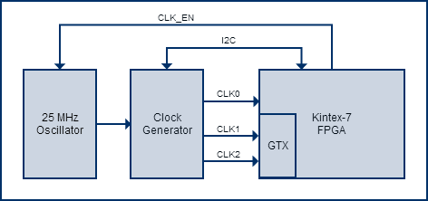
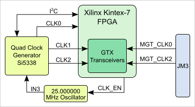
Figure 3: Clock Generator Clocking block diagram.
| I/O Si5338A (U2) | Default Frequency | Notes |
|---|---|---|
IN1/IN2 | - | Not used (external clock signal supply). |
IN3 | 25MHz | Fixed input clock signal from. reference clock generator SiT8208AI (U3). |
IN4 | - | LSB of the default I2C-Adress 0x70. |
IN5/IN6 | - | Not used (external clock signal supply). |
CLK0 A/B | 100 MHz | Bank 14 clock input, Pins: B14_L12_P, B14_L12_N |
CLK1 A/B | 125MHz | MGT reference clock 1 to FPGA Bank 116 MGT |
CLK2 A/B | 125MHz- | MGT reference clock 3 to FPGA Bank 115 MGT |
| CLK3 | - | not used |
Table 7: Pin description of Si5338A PLL clock generator Si5338A.
32 MByte Quad SPI Flash Memory
...
| Note |
|---|
SPI Flash QE (Quad Enable) bit must be set, or the FPGA would not configure itself from Flash. This bit is always set at the manufacturing. |
| Page break |
|---|
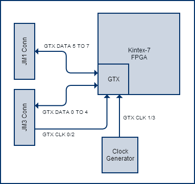
GTX Transceivers
The Kintex-7 device that is used on the TE0741 board has 8 GTX transceivers. All 8 are wired directly to connectors JM1 and JM3. There are also 4 clocks that are associated with the transceivers. Two of the clocks are connected directly to JM3, whilst the other two are derived from the clock generator. As there is no capacitive coupling of the data and clock lines that are connected to the connectors, these may be required on the user’s PCB depending on the application.
To enable the voltage supply for the GTX transceivers, namely the Enpirion EP53F8QI voltage regulators U6 and U16, which serve the voltages MGTAVCC (1.0 V) and MGTAVTT (1.2 V), the signal EN_MGT (bank 14, pin H22) have to be set high. The voltage regulators will indicate "Power OK" with signals PG_MGT_1V and PG_MGT_1V2, when reaching stable state.
![]()
Figure 4: GTX Transceiver transceiver block diagram.
Page break
System Controller CPLD
The system controller System Controller CPLD is used to coordinate the configuration of the FPGA. The FPGA is held in reset (by driving the PROG_B signal) until the power supplies have sequenced. Setting input signal RESIN low will also reset the FPGA. This signal can be driven from the user’s PCB via the board connector.
It is possible for the user to create their own system controller User can create its own System Controller CPLD design using the Lattice Diamond software . Once created the design can be programmed and program it into the device using the JTAG pinsinterface. The JTAGMODE signal JTAGMODE should be set to 3.3V to enable programming mode. For , for normal module operation it should be set to 0V.
The LED that is Green LED D4 (C_LED) connected to the system controller flashes System Controller CPLD is to indicate the state status of the boardmodule. CPLD Firmware, see TE0741 CPLD.
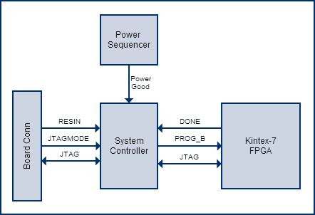
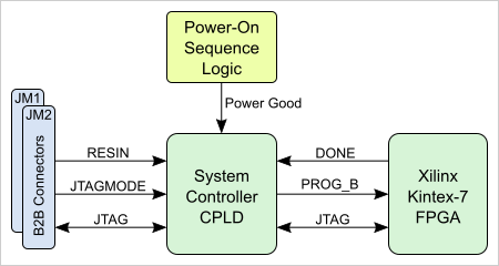
Figure 5: System Controller CPLD block diagram.
Power and Power-On Sequence
...
Power Consumption
| Power Input Pin | Max Typical Current |
|---|---|
| VIN | TBD* |
| 3.3VIN | TBD* |
Table 8: maximal Maximum current of power supplys supplies.
* TBD - To Be Determined soon with reference design setup.
Lowest power consumption is achieved when powering the module from single 3.3V supply. When using split 3.3V/5V supplies the power consumption (and heat dissipation) will rise, this is due to the DC/DC converter efficiency (it decreases when VIN/VOUT ratio rises).
Power-On Sequence
For highest efficiency of on board DC/DC regulators, it is recommended to use same 3.3V power source for both VIN and 3.3VIN power rails. Although VIN and 3.3VIN can be powered up in any order, it is recommended to power them up simultaneously.
It is important that all baseboard I/O's are 3-stated at power-on until System Controller sets PGOOD signal high (B2B connector JM1, pin 30), or 3.3V is present on B2B connector JM2 pins 10,12 or 91, meaning that all on-module voltages have become stable and module is properly powered up.
See Xilinx datasheet DS182 (for Kintex7) for additional information. User should also check related baseboard documentation when choosing baseboard design for TE0741 module.
The FPGA 1.0V supply is derived from two regulators operating in a parallel allowing higher load currents. To start the power-on sequence, pin EN1 (JM1-28, enable 1.0V voltage regulators) is by default high. By driving EN1 pin low on base-board the power-on sequence will not start until the EN1 pin is released to high.
A 3.3V supply is also needed and must be supplied from the user's PCB. An output 3.3V supply is available on some of the board connector pins (see section 'Power Rails'). The input 3.3VIN will be switched to the internal 3.3V voltage level after the FPGA 1.0V supply is stable. Than this power supply will be available on the B2B connector pins.
The regulators can be powered from the 3.3V supply or a 5V supply if preferred. The options for powering the board are detailed below.
- Apply 5V to pins VIN and 3.3V to pins 3.3VIN on the board connector
- Apply 3.3V to pins VIN and 3.3VIN on the board connectors.
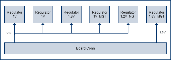
Figure 6: Connections between the on-board DCDC and LDO regulators.
Power Rails
...
Voltages on B2B-
Connectors
...
1, 3, 5
...
Table 9: Power rails of SoM on B2B connectors.
Bank Voltages
...
Table 10: Range of FPGA's bank voltages.
See the Kintex-7 datasheet (DS182) for the allowable voltage range.
Board to Board Connectors
...
Variants Currently In Production
...
Designator /
Module Variant
...
U1
...
Table 11: Differences between variants of Module TE0741.
Technical Specifications
Absolute Maximum Ratings
...
VIN supply voltage
...
-0.1
...
-0.5
...
-55
...
+125
...
Table 12: Absolute maximum ratings.
| Note |
|---|
| Assembly variants for higher storage temperature range are available on request. |
Recommended Operation Conditions
...
3,3V ± 5%
...
I/O banks (VCCO)
...
.
Lowest power consumption is achieved when powering the module from single 3.3V supply. When using split 3.3V/5V power supplies, the power consumption (and heat dissipation) will rise, this is due to the DC-DC converter efficiency (it decreases when VIN/VOUT ratio rises).
Power-On Sequence
For highest efficiency of on board DC-DC regulators, it is recommended to use same 3.3V power source for both VIN and 3.3VIN power rails. Although VIN and 3.3VIN can be powered up in any order, it is recommended to power them up simultaneously.
It is important that all baseboard I/Os are 3-stated at power-on until System Controller sets PGOOD signal high (B2B connector JM1, pin 30), or 3.3V is present on B2B connector JM2 pins 10,12 or 91, meaning that all on-module voltages have become stable and module is properly powered up.
See Xilinx datasheet DS182 for additional information. User should also check related baseboard documentation when choosing baseboard design for TE0741 module.
The FPGA 1.0V supply is derived from two regulators operating in a parallel allowing higher load currents. To start the power-on sequence, pin EN1 (JM1-28, enable 1.0V voltage regulators) is by default high. By driving EN1 pin low on base-board the power-on sequence will not start until the EN1 pin is released to high.
| Page break |
|---|
Power Rails
Voltages on B2B-Connectors | B2B JM1 Pin | B2B JM2 Pin | B2B Direction | Note |
|---|---|---|---|---|
| VIN | 1, 3, 5 | 2, 4, 6, 8 | Input | Supply voltage. |
| 3.3VIN | 13, 15 | - | Input | Supply voltage. |
| VCCIO12 | - | 7, 9 | Input | High range bank voltage. |
| VCCIO13 | 9, 11 | - | Input | High range bank voltage. |
| VCCIO15 | - | 5 | Input | High range bank voltage. |
| VCCIO16 | - | 1, 3 | Input | High range bank voltage. |
| 3.3V | - | 10, 12, 91 | Output | Internal 3.3V voltage level. |
Table 9: Power rails of SoM on B2B connectors.
Bank Voltages
| Bank | Schematic Name | Voltage | Range |
|---|---|---|---|
| 0 Config | 3.3V | 3.3V | - |
| 12 | VCCIO12 | user | HR: 1.2V to 3.3V |
| 13 | VCCIO13 | user | HR: 1.2V to 3.3V |
| 14 | 3.3V | 3.3V | - |
| 15 | VCCIO15 | user | HR: 1.2V to 3.3V |
| 16 | VCCIO16 | user | HR: 1.2V to 3.3V |
Table 10: Range of FPGAs bank voltages.
See Xilinx Kintex-7 datasheet DS182 for the voltage ranges allowed.
Board to Board Connectors
| Include Page | ||||
|---|---|---|---|---|
|
Variants Currently In Production
Module Variant | FPGA | U15 | FPGA Junction Temperature | Temperature Grade |
|---|---|---|---|---|
| TE0741-03-070-2CF | XC7K70T-2FBG676C | - | 0°C to 85°C | Commercial grade |
| TE0741-03-070-2IF | XC7K70T-2FBG676I | - | -40°C to 100°C | Industrial grade |
| TE0741-03-160-2CF | XC7K160T-2FBG676C | - | 0°C to 85°C | Commercial grade |
| TE0741-03-160-2C1 | XC7K160T-2FFG676C | - | 0°C to 85°C | Commercial grade |
| TE0741-03-160-2IF | XC7K160T-2FBG676I | - | -40°C to 100°C | Industrial grade |
| TE0741-03-325-2CF | XC7K325T-2FBG676C | EN63A0QI | 0°C to 85°C | Commercial grade |
| TE0741-03-325-2IF | XC7K325T-2FBG676I | EN63A0QI | -40°C to 100°C | Industrial grade |
| TE0741-03-410-2CF | XC7K325T-2FBG676C | EN63A0QI | 0°C to 85°C | Commercial grade |
Table 11: Module TE0741-03 variants.
Technical Specifications
Absolute Maximum Ratings
| Parameter | Min | Max | Units | Notes |
|---|---|---|---|---|
VIN supply voltage | -0.3 | 6.5 | V | - |
| 3.3VIN supply voltage | -0.1 | 3.6 | V | - |
| PL IO bank supply voltage for HR I/O banks (VCCO) | -0.5 | 3.6 | V | - |
| I/O input voltage for HR I/O banks | -0.4 | VCCO_X+0.55 | V | - |
| GT receiver (RXP/RXN) and transmitter (TXP/TXN) | -0.5 | 1.26 | V | Xilinx datasheet DS182 |
| Voltage on module JTAG pins | -0.5 | VCCO_0+0.45 | V | VCCO_0 is 3.3V nominal. |
| Storage temperature | -55 | +125 | °C | - |
Table 12: Absolute maximum ratings.
Recommended Operating Conditions
| Parameter | Min | Max | Units | Notes | Reference Document |
|---|---|---|---|---|---|
| VIN supply voltage | 2.4 | 5.5 | V | - | EP53F8QI data sheet |
| 3.3VIN supply voltage | 3.135 | 3.465 | V | 3,3V ± 5% | - |
| PL I/O bank supply voltage for HR I/O banks (VCCO) | 1.14 | 3.465 | V | - | Xilinx datasheet DS182 |
| I/O input voltage for HR I/O banks | -0.20 | VCCO+0.2 | V | - | Xilinx datasheet DS182 |
| GT receiver (RXP/RXN) and transmitter (TXP/TXN) | (*) | (*) | - | - | * See datasheet DS182 |
| Voltage on module JTAG pins | 3.135 | 3.465 | V | - | - |
Table 13: Recommended operation conditions.
Operating Temperature Ranges
Commercial grade: 0°C to +70°C.
Industrial grade: -40°C to +85°C.
The module operating temperature range depends also on customer design and cooling solution. Please contact us for options.
| Note |
|---|
| Check Xilinx datasheet DS182 for complete list of absolute maximum and recommended operating ratings. |
Physical Dimensions
- Module size: 50 mm × 40 mm
- Mating height with standard connectors: 8mm
- PCB thickness: 1.6mm
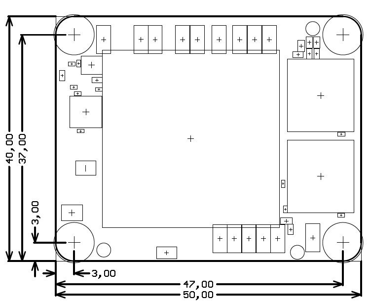
Figure 6: Physical dimensions of the TE0741 module. All dimensions are shown in millimeters.
Weight
19 g - Plain module.
8.8 g - Set of nuts and bolts.
Revision History
Hardware Revision History
| Date | Revision | Notes | PCN | Documentation |
|---|---|---|---|---|
| 2016-10-25 | 03 | 1) Fixed DC-DC connection for parallel operation 2) Samtec Razor Beam connectors updated 3) Serial number (traceability) pad added 4) Changed ferrite beads L1..L4 size 0402 to BKP0603HS121-T 5) Thermal vias added to mounting holes | PCN-20170106 | TE0741-03 |
| 2013-11-06 | 02 |
| TE0741-02 | |
| 01 | First production release |
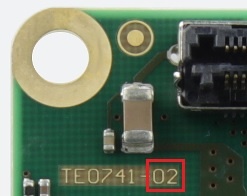
Hardware revision number is written on the PCB board together with the module model number separated by the dash.


Figure 7: TE0741 PCB revision number.
Document Change History
| Date | Revision | Contributors | Description | ||||||||||||||||||||||||||
|---|---|---|---|---|---|---|---|---|---|---|---|---|---|---|---|---|---|---|---|---|---|---|---|---|---|---|---|---|---|
|
|
|
| ||||||||||||||||||||||||||
| 2018-08-29 | v.64 | John Hartfiel |
| ||||||||||||||||||||||||||
2017-11-10 | v.63 | John Hartfiel |
| ||||||||||||||||||||||||||
| 2017-08-28 | v.60 | Jan Kumann |
| ||||||||||||||||||||||||||
| 2017-07-20 | v.57 | John Hartfiel |
| ||||||||||||||||||||||||||
| 2017-06-07 | v.55 | Jan Kumann |
| ||||||||||||||||||||||||||
| 2017-06-02 | v.50 | Jan Kumann |
| ||||||||||||||||||||||||||
| 2017-01-22 | v.42 | Jan Kumann |
| ||||||||||||||||||||||||||
| 2017-01-13 | v.38 | Jan Kumann |
| ||||||||||||||||||||||||||
| 2017-01-12 | v.21 | John Hartfiel |
| ||||||||||||||||||||||||||
| 2016-12-14 | v.19 | Ali Naseri |
| ||||||||||||||||||||||||||
| 2013-12-02 | v.1 | Antti Lukats, Jon Bean |
|
Table 13: Recommended operation conditions.
| Note |
|---|
| Please check Xilinx datasheet (DS182) for complete list of absolute maximum and recommended operating ratings. |
Physical Dimensions
- Module size: 50 mm × 40 mm
- Mating height with standard connectors: 8mm
- PCB thickness: 1.6mm
All dimensions are shown in mm.
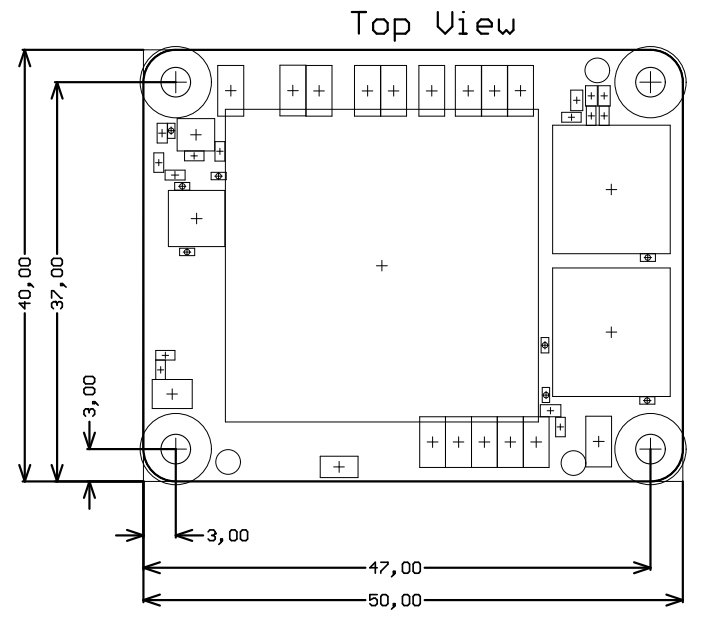

Figure 7: Physical Dimensions of the TE0741-02 board.
Operating Temperature Ranges
Commercial grade: 0°C to +70°C.
Industrial grade: -40°C to +85°C.
The module operating temperature range depends also on customer design and cooling solution. Please contact us for options.
Weight
...
Revision History
Hardware Revision History
...
- improved power-sequencing
- added differential terminator
to bank 14 clock input
...
Hardware revision number is printed on the PCB board together with the module model number separated by the dash.
Document Change History
TRM revision
Disclaimer
| Include Page | ||||
|---|---|---|---|---|
|
Overview
Content Tools