...
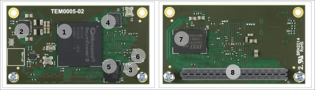
The Trenz Electronic TEM0005-02 is a low-cost , small FPGA module with Microsemi SmartFusion2 FPGA SoC and 32 MByte flash memory for configuration and operation. SmartFusion2 combines a 166 MHz Cortex-M3 MCU with 256 KByte Flash and 80 KByte SRAM as well as 12 kLUT FPGA Core Logic.
...
- SoC/FPGA
- Package: VFG400
- Device: M2S005, M2S010, M2S025, M2S050 ,M2S060 *
- Engine: VFG166Mhz 32Bit ARM Cortex-M3
- Speed: -1, Standard*, **
- Temperature: C, I,*, **
- RAM/Storage
- Low Power DDR3
- Data width: 8/ 16bit
- Size: def. 2Gb*
- Speed: 20ns***
QSPIData width: 8 bit - SPI Flash
- 2Kb EEPROM
- On Board
- Crypto Authentication IC
- Voltage monitor IC
- 10/100 Mbps PHY Ethernet
- Interface
- Power
- 5V 3.3V supplied from carrier
- Dimension
- Notes
- * depends on assembly version** also non low power assembly options possible
- *** depends on used FPGA and DDR3 combination
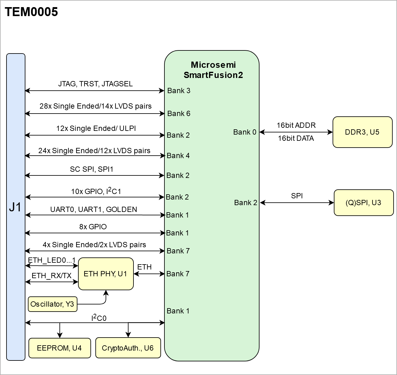
Block Diagram
| Page properties |
|---|
|
add drawIO object here.
|
...
| Scroll Title |
|---|
| anchor | Figure_OV_BD |
|---|
| title | TEM0005 block diagram |
|---|
|
| Scroll Ignore |
|---|
| scroll-pdf | true |
|---|
| scroll-office | true |
|---|
| scroll-chm | true |
|---|
| scroll-docbook | true |
|---|
| scroll-eclipsehelp | true |
|---|
| scroll-epub | true |
|---|
| scroll-html | true |
|---|
| | draw.io Diagram |
|---|
| border | false |
|---|
| |
|---|
| diagramName | TEM0005_OV_BD |
|---|
| simpleViewer | false |
|---|
| width | 639 |
|---|
| links | auto |
|---|
| tbstyle | hidden |
|---|
| diagramDisplayName | |
|---|
| lbox | true |
|---|
| diagramWidth | 641 |
|---|
| revision | 912 |
|---|
|
|
| Scroll Only |
|---|
|
|
Main Components
...
| Scroll Title |
|---|
| anchor | Figure_OV_MC |
|---|
| title | TEM0005 main components |
|---|
|
| Scroll Ignore |
|---|
| draw.io Diagram |
|---|
| border | false |
|---|
| |
|---|
| diagramName | TEM0005_OV_MC |
|---|
| simpleViewer | false |
|---|
| width | 600 |
|---|
| links | auto |
|---|
| tbstyle | hidden |
|---|
| diagramDisplayName | |
|---|
| lbox | true |
|---|
| diagramWidth | 641 |
|---|
| revision | 20 |
|---|
|
|
| Scroll Only |
|---|
|
|
- Microsemi SmartFusionSmartFusion2 SoC, U2
- RegDual DCDC Regulator, U7
- EEPROM, U4
- 10/100 Mb Ethernet, U1
- QSPI Flash, U3
- Authentication IC, U6
- DDR3 Memory, U5
- B2B Connector, J1
...
| Scroll Title |
|---|
| anchor | Table_OV_IDS |
|---|
| title | Initial delivery state of programmable devices on the module |
|---|
|
| Scroll Table Layout |
|---|
| orientation | portrait |
|---|
| sortDirection | ASC |
|---|
| repeatTableHeaders | default |
|---|
| style | |
|---|
| widths | |
|---|
| sortByColumn | 1 |
|---|
| sortEnabled | false |
|---|
| cellHighlighting | true |
|---|
|
Storage device name | Content | Notes |
|---|
Quad SPI Flash | Not Programmed |
| | EEPROM | Not Programmed |
| | DDR3 SDRAMCryptoAuthentication | Not Programmed |
|
|
Configuration Signals
...
| Scroll Title |
|---|
| anchor | Table_SIP_B2B |
|---|
| title | General PL I/O to B2B connectors information |
|---|
|
| Scroll Table Layout |
|---|
| orientation | portrait |
|---|
| sortDirection | ASC |
|---|
| repeatTableHeaders | default |
|---|
| style | |
|---|
| widths | |
|---|
| sortByColumn | 1 |
|---|
| sortEnabled | false |
|---|
| cellHighlighting | true |
|---|
|
| FPGA Bank | Interface | I/O Signal Count | Voltage Level | Notes |
|---|
| Bank 01 | GPIO | 8x Single Ended | 3.3V |
| | UART | 4x Single Ended | 3.3V |
| | I2C | 2x Single Ended | 3.3V |
| | GOLDEN | 1x Single Ended | 3.3V |
| | Bank 2 | ULPI/I/O | 12x Single Ended | 3.3V |
| | I2C | 2x Single Ended | 3.3V |
| | GPIO | 10x Single Ended | 3.3V |
| | SC SPI | 4x Single Ended | 3.3V | SPI0 | 4x Single Ended |
| | 3.3V | SPI1 | 7x Single Ended | 3.3V |
| | Bank 3 | JTAG | 5x Single Ended | 3.3V |
| | Reset | 1x Single Ended | 3.3V |
| | Bank 4 | I/O | 24x Single Ended/12 LVDS pairs | 3.3V |
| | Bank 6 | I/O | 24x 28x Single Ended3.3V/14 LVDS pairs | VDDI6 | max 2.5V | | Bank 7 | I/O | 4x Single Ended | 3.3V |
|
|
...
| Scroll Title |
|---|
| anchor | Table_SIP_JTG |
|---|
| title | JTAG pins connection |
|---|
|
| Scroll Table Layout |
|---|
| orientation | portrait |
|---|
| sortDirection | ASC |
|---|
| repeatTableHeaders | default |
|---|
| style | |
|---|
| widths | |
|---|
| sortByColumn | 1 |
|---|
| sortEnabled | false |
|---|
| cellHighlighting | true |
|---|
|
JTAG Signal | B2B Connector |
|---|
| TMS | J1-14 | | TDI | J1-8 | | TDO | J1-10 | | TCK | J1-12 | | JTAG_ENTRST | J1-7 |
|
Test Points
| Page properties |
|---|
|
you must fill the table below with group of Test Point which are indicated as TP in a schematic. If there is no Test Point remarked in the schematic, delet the Test Point section. Example: | Test Point | Signal | B2B | Notes |
|---|
| 10 | PWR_PL_OK | J2-120 |
|
|
...
| Scroll Title |
|---|
| anchor | Table_OBP |
|---|
| title | On board peripherals |
|---|
|
| Scroll Table Layout |
|---|
| orientation | portrait |
|---|
| sortDirection | ASC |
|---|
| repeatTableHeaders | default |
|---|
| style | |
|---|
| widths | |
|---|
| sortByColumn | 1 |
|---|
| sortEnabled | false |
|---|
| cellHighlighting | true |
|---|
|
|
(Quad) SPI Flash Memory
| Page properties |
|---|
|
Notes : Minimum and Maximum density of quad SPI flash must be mentioned for other assembly options. |
The TEM0005 is equipped with a QSPI (Q)SPI flash memory, U3 provided in order to store data and configuration.
...
The TEM0005 is equipped with an EEPROM IC, U4. The two I2C signals are connected to authentication IC as well.
...
There is an Authentication IC ATECC608A provided on TEM0005, The IC is connected to I2C0 signalsbus.
| Scroll Title |
|---|
| anchor | Table_OBP_Auth |
|---|
| title | Authentication IC information |
|---|
|
| Scroll Table Layout |
|---|
| orientation | portrait |
|---|
| sortDirection | ASC |
|---|
| repeatTableHeaders | default |
|---|
| style | |
|---|
| widths | |
|---|
| sortByColumn | 1 |
|---|
| sortEnabled | false |
|---|
| cellHighlighting | true |
|---|
|
| Pin | Schematic | Notes |
|---|
| SCL | I2C0_SCL | Serial Clock | | SDA | I2C1_SCL | Serial Data |
|
DDR3L SDRAM
| Scroll Title |
|---|
| anchor | Table_OBP_I2C_Authentication IC |
|---|
| title | I2C address for Authentication IC |
|---|
|
| Scroll Table Layout |
|---|
| orientation | portrait |
|---|
| sortDirection | ASC |
|---|
| repeatTableHeaders | default |
|---|
| style | |
|---|
| widths | |
|---|
| sortByColumn | 1 |
|---|
| sortEnabled | false |
|---|
| cellHighlighting | true |
|---|
|
| Pin | I2C Address | Designator | Notes |
|---|
| SCL/SDA | 0xC0 | U6 | This is the default value, which can be changed, see device datasheet. |
|
DDR3L SDRAM
| Page properties |
|---|
|
| Page properties |
|---|
|
Notes : Minimum and Maximum density of DDR3 SDRAM must be mentioned for other assembly options. (pay attention to supported address length for DDR3) |
...
- Part number: IS43TR16128CL-125KBLI
- Supply voltage: 1.5 VAccess: time 20 ns
- Temperature: -40 to 95 °C
...
| Scroll Title |
|---|
| anchor | Table_OBP_CLK |
|---|
| title | Osillators |
|---|
|
| Scroll Table Layout |
|---|
| orientation | portrait |
|---|
| sortDirection | ASC |
|---|
| repeatTableHeaders | default |
|---|
| style | |
|---|
| widths | |
|---|
| sortByColumn | 1 |
|---|
| sortEnabled | false |
|---|
| cellHighlighting | true |
|---|
|
| Designator | Description | Frequency | Note |
|---|
| Y3 | Crystal Oscillator25 MHz | 25 MHz | Connected to ETH PHY |
|
Power and Power-On Sequence
| Page properties |
|---|
|
In 'Power and Power-on Sequence' section there are three important digrams which must be drawn: - Power on-sequence
- Power distribution
- Voltage monitoring circuit
|
Power Supply
Power supply with minimum current capability of 1.5 A for system startup is recommended.
...
Power Supply
Power supply with minimum current capability of 1.5 A for system startup is recommended.
Power Consumption
| Scroll Title |
|---|
| anchor | Table_PWR_PC |
|---|
| title | Power Consumption |
|---|
|
| Scroll Table Layout |
|---|
| orientation | portrait |
|---|
| sortDirection | ASC |
|---|
| repeatTableHeaders | default |
|---|
| style | |
|---|
| widths | |
|---|
| sortByColumn | 1 |
|---|
| sortEnabled | false |
|---|
| cellHighlighting | true |
|---|
|
| Power Input Pin | Typical Current |
|---|
| VIN | TBD* |
|
* TBD - To Be Determined
Power Distribution Dependencies
| Scroll Title |
|---|
| anchor | TableFigure_PWR_PCPD |
|---|
| title | Power ConsumptionDistribution |
|---|
|
tablelayout |
| orientation | portrait |
|---|
| sortDirection | ASC |
|---|
| repeatTableHeaders | default |
|---|
style | widths | | sortByColumn | 1 |
|---|
| sortEnabled | false |
|---|
| cellHighlighting | true |
|---|
| Power Input Pin | Typical Current |
|---|
| VIN | TBD* |
* TBD - To Be Determined
...
| ignore |
|---|
| draw.io Diagram |
|---|
| border | false |
|---|
| |
|---|
| diagramName | TEM0005_PWR_PD |
|---|
| simpleViewer | false |
|---|
| width | 639 |
|---|
| links | auto |
|---|
| tbstyle | hidden |
|---|
| diagramDisplayName | |
|---|
| lbox | true |
|---|
| diagramWidth | 640 |
|---|
| revision | 5 |
|---|
|
|
| Scroll Only |
|---|
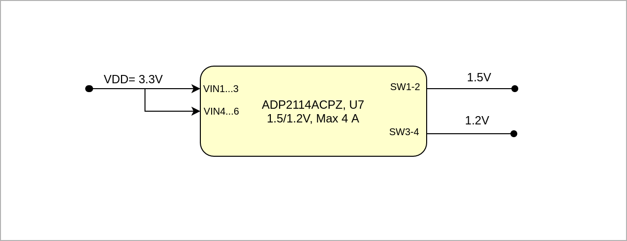 Image Added Image Added
|
|
Power-On Sequence
| Scroll Title |
|---|
| anchor | Figure_PWR_PDPS |
|---|
| title | Power DistributionSequency |
|---|
|
| Scroll Ignore |
|---|
| draw.io Diagram |
|---|
| border | false |
|---|
| |
|---|
| diagramName | TEM0005_PWR_PDPS |
|---|
| simpleViewer | false |
|---|
| width | 639 |
|---|
| links | auto |
|---|
| tbstyle | hidden |
|---|
| diagramDisplayName | |
|---|
| lbox | true |
|---|
| diagramWidth | 641 |
|---|
| revision | 3 |
|---|
|
|
| Scroll Only |
|---|
Image Removed |
|
Power-On Sequence
| Scroll Only |
|---|
 Image Added Image Added
|
|
Voltage Monitor Circuit
The TEM0005 is equipped with a voltage monitoring IC, U8. Reset Logic Output (nRST) asserts low when any of the V1, V2, or ADJ inputs are below their reset thresholds.
| scroll-scroll-title |
|---|
| anchor | Figure_PWR_PSVMC |
|---|
| title | Power SequencyVoltage Monitor Circuit |
|---|
|
| Scroll Ignore |
|---|
| draw.io Diagram |
|---|
| border | false |
|---|
| |
|---|
| diagramName | TEM0005_PWR_PSVMC |
|---|
| simpleViewer | false |
|---|
| width | 639 |
|---|
| links | auto |
|---|
| tbstyle | hidden |
|---|
| diagramDisplayName | |
|---|
| lbox | true |
|---|
| diagramWidth | 641 |
|---|
| revision | 2 |
|---|
|
|
| Scroll Only |
|---|
Image Removed |
|
Voltage Monitor Circuit
|
| Scroll Title |
|---|
| anchor | Figure_PWR_VMC |
|---|
| title | Voltage Monitor Circuit |
|---|
|
| Scroll Ignore |
|---|
| Create DrawIO object here: Attention if you copy from other page, objects are only linked. |
| Scroll Only |
|---|
image link to the generate DrawIO PNG file of this page. This is a workaround until scroll pdf export bug is fixed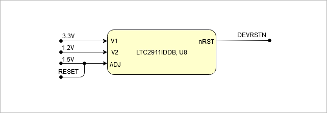 Image Added Image Added |
|
Power Rails
| Scroll Title |
|---|
| anchor | Table_PWR_PR |
|---|
| title | Module power rails. |
|---|
|
| Scroll Table Layout |
|---|
| orientation | portrait |
|---|
| sortDirection | ASC |
|---|
| repeatTableHeaders | default |
|---|
| style | |
|---|
| widths | |
|---|
| sortByColumn | 1 |
|---|
| sortEnabled | false |
|---|
| cellHighlighting | true |
|---|
|
| Power Rail Name | B2B Connector JM1 J1 Pin | Direction | Notes |
|---|
| 3.3V | 1, 2, 3, 4 | OutputInput |
| | VDDI6 | 22 | Input |
|
|
Bank Voltages
| Scroll Title |
|---|
| anchor | Table_PWR_BV |
|---|
| title | Zynq SoC bank voltages. |
|---|
|
| Scroll Table Layout |
|---|
| orientation | portrait |
|---|
| sortDirection | ASC |
|---|
| repeatTableHeaders | default |
|---|
| style | |
|---|
| widths | |
|---|
| sortByColumn | 1 |
|---|
| sortEnabled | false |
|---|
| cellHighlighting | true |
|---|
|
| Schematic Name | | Notes |
|---|
| Bank0 | VDDI01.5V | 1.5V |
| | Bank1 | VDDI13.3V | 3.3V |
| | Bank2VDDI2 | 3.3V | 3.3V |
| | Bank3VDDI3 | 3.3V | 3.3V |
| | Bank4VDDI4 | 3.3V | 3.3V |
| | Bank5 | 3.3V | VDDI6 | 3.3V |
| | Bank6 | VDDI6 | 3.3Vmax. 2.5V | supplied by carrier | | Bank7VDDI7 | 3.3V | 3.3V |
|
|
Board to Board Connectors
| Page properties |
|---|
|
- This section is optional and only for modules.
use "include page" macro and link to the general B2B connector page of the module series, For example: 6 x 6 SoM LSHM B2B Connectors
| Include Page |
|---|
| PD:6 x 6 SoM LSHM B2B ConnectorsPD: |
|---|
| 6 x 6 SoM LSHM B2B Connectors |
|---|
|
|
| Include Page |
|---|
| DRAFT:3.1 x 5.6 SoM ST5/SS5 B2B Connectors |
|---|
| DRAFT:3.1 x 5.6 SoM ST5/SS5 B2B Connectors |
|---|
|
...
| Scroll Title |
|---|
| anchor | Table_TS_AMR |
|---|
| title | PS absolute maximum ratings |
|---|
|
| Scroll Table Layout |
|---|
| orientation | portrait |
|---|
| sortDirection | ASC |
|---|
| repeatTableHeaders | default |
|---|
| style | |
|---|
| widths | |
|---|
| sortByColumn | 1 |
|---|
| sortEnabled | false |
|---|
| cellHighlighting | true |
|---|
|
| Symbols | Description | Min | Max | Unit |
|---|
| VIN | Input Supply Voltage | -0.3 | 3.63 | V | | STG_T | Storage Temperature | -45 | 125 | °C |
|
Recommended Operating Conditions
...
| Scroll Title |
|---|
| anchor | Table_TS_ROC |
|---|
| title | Recommended operating conditions. |
|---|
|
| Scroll Table Layout |
|---|
| orientation | portrait |
|---|
| sortDirection | ASC |
|---|
| repeatTableHeaders | default |
|---|
| style | |
|---|
| widths | |
|---|
| sortByColumn | 1 |
|---|
| sortEnabled | false |
|---|
| cellHighlighting | true |
|---|
|
| Parameter | Min | Max | Units | Reference Document |
|---|
| VIN | 3.15 | 3.45 | V | See the carrier datasheets. | | OPT_T | 0 /-4540 | 12585 | °C | See Microsemi Smartfusion2 datasheet. Depends on assembly version. |
|
Physical Dimensions
Module size: 56 mm × 31 mm. Please download the assembly diagram for exact numbers.
Mating height with standard connectors: 4 mm.
...
| Scroll Title |
|---|
| anchor | Table_RH_HRH |
|---|
| title | Hardware Revision History |
|---|
|
| Scroll Table Layout |
|---|
| orientation | portrait |
|---|
| sortDirection | ASC |
|---|
| repeatTableHeaders | default |
|---|
| style | |
|---|
| widths | |
|---|
| sortByColumn | 1 |
|---|
| sortEnabled | false |
|---|
| cellHighlighting | true |
|---|
|
| Date | Revision | Changes | Documentation Link |
|---|
| 2019-10-01 | REV01 | | REV01 | | 2020-05-20 | REV02 | - Support M2S050 -> added >added R29,R30, C24..C26,C31
- Added resistor R32
- Full upd LIB
| REV02 |
|
...
| Scroll Title |
|---|
| anchor | Table_RH_DCH |
|---|
| title | Document change history. |
|---|
|
| Scroll Table Layout |
|---|
| orientation | portrait |
|---|
| sortDirection | ASC |
|---|
| repeatTableHeaders | default |
|---|
| style | |
|---|
| widths | |
|---|
| sortByColumn | 1 |
|---|
| sortEnabled | false |
|---|
| cellHighlighting | true |
|---|
|
| Date | Revision | Contributor | Description |
|---|
| Page info |
|---|
| infoType | Modified date |
|---|
| dateFormat | yyyy-MM-dd |
|---|
| type | Flat |
|---|
|
| | Page info |
|---|
| infoType | Current version |
|---|
| prefix | v. |
|---|
| type | Flat |
|---|
| showVersions | false |
|---|
|
| | Page info |
|---|
| infoType | Modified by |
|---|
| type | Flat |
|---|
| showVersions | false |
|---|
|
| | -- | all | | Page info |
|---|
| infoType | Modified users |
|---|
| type | Flat |
|---|
| showVersions | false |
|---|
|
| |
|
...