Page History
Template Revision 2.12
...
| HTML |
|---|
<!-- tables have all same width (web max 1200px and pdf full page(640px), flexible width or fix width on menu for single column can be used as before) -->
<style>
.wrapped{
  width: 100% !important;
  max-width: 1200px !important;
 }
</style> |
...
| hidden | true |
|---|---|
| id | Comments |
Important General Note:
...
Designate all graphics and pictures with a number and a description, Use "Scroll Title" macro
...
Figure template:
...
| anchor | Figure_anchorname |
|---|---|
| title | Text |
| Scroll Ignore |
|---|
Create DrawIO object here: Attention if you copy from other page, objects are only linked. |
| Scroll Only |
|---|
image link to the generate DrawIO PNG file of this page. This is a workaround until scroll pdf export bug is fixed |
...
Table template:
- Layout macro can be use for landscape of large tables
...
| anchor | Table_tablename |
|---|---|
| title | Text |
...
The anchors of the Scroll Title should be named consistant across TRMs. A incomplete list of examples is given below
<type>_<main section>_<name>
- type: Figure, Table
- main section:
- "OV" for Overview
- "SIP" for Signal Interfaces and Pins,
- "OBP" for On board Peripherals,
- "PWR" for Power and Power-On Sequence,
- "B2B" for Board to Board Connector,
- "TS" for Technical Specification
- "VCP" for Variants Currently in Production
- "RH" for Revision History
- name: custom, some fix names, see below
- Fix names:
"Figure_OV_BD" for Block Diagram
"Figure_OV_MC" for Main Components
"Table_OV_IDS" for Initial Delivery State
"Table_PWR_PC" for Power Consumption
- "Figure_PWR_PD" for Power Distribution
- "Figure_PWR_PS" for Power Sequence
- "Figure_PWR_PM" for Power Monitoring
- "Table_PWR_PR" for Power Rails
- "Table_PWR_BV" for Bank Voltages
"Table_TS_AMR" for Absolute_Maximum_Ratings
"Table_TS_ROC" for Recommended_Operating_Conditions
- "Figure_TS_PD" for Physical_Dimensions
- "Table_VCP_SO" for TE_Shop_Overview
"Table_RH_HRH" for Hardware_Revision_History
- "Figure_RH_HRN" for Hardware_Revision_Number
- "Table_RH_DCH" for Document_Change_History
...
| Page properties | ||||
|---|---|---|---|---|
| ||||
----------------------------------------------------------------------- |
| Page properties | ||||
|---|---|---|---|---|
| ||||
Note for Download Link of the Scroll ignore macro:
|
| Scroll Ignore |
|---|
| Scroll pdf ignore | |
|---|---|
Table of Contents
|
Overview
Trenz Electronic TEM0007 module is an industrial-grade FPGA micromodule integrating a Microsemi Polarfire SoC FPGA, Gigabit Ethernet PHY, USB PHY 2.0, one GByte LPDDR4 SDRAM, 64 MByte SPI Flash memory for configuration and operation, and power supply. A large number of configurable I/Os is provided via robust board-to-board (B2B) connectors.
Refer to http://trenz.org/tem0007-info for the current online version of this manual and other available documentation.
| Page properties | ||||
|---|---|---|---|---|
| ||||
Notes :
|
Key Features
...
| hidden | true |
|---|---|
| id | Comments |
Note:
'description: Important components and connector or other Features of the module
→ please sort and indicate assembly options
Key Features' must be split into 6 main groups for modues:
- SoC/FPGA
- Package:
- Speed:
- Temperature:
- RAM/Storage
- E.g. SDRAM, SPI
- On Board
- E.g. CPLD, PLL
- Interface
- E.g. ETH, USB, B2B, Display port
- Power
- E.g. Input supply voltage
- Dimension
Key Features' must be split into 6 main groups for carrier:
- Modules
- TE0808, TE807, TE0803,...
- RAM/Storage
- E.g. SDRAM, SPI
- On Board
- E.g. CPLD, PLL
- Interface
- E.g. ETH, USB, B2B, Display port
- Power
- E.g. Input supply voltage
- Dimension
- SoC/FPGA
- Industrial-grade Microsemi Polarfire SoC MPFS250T-1FCVG484I
- RAM/Storage
- 1 GByte LPDDR4
- 64 MByte SPI Flash Memory
- On Board
- System Controller CPLD
- MAC address serial EEPROM
- Interface
- 10/100/1000 Mbps Gigabit Ethernet PHY
- Highly Integrated Full-Featured Hi-Speed USB 2.0 ULPI Transceiver
- Trenz 4 x 5 module socket connectors (3 x Samtec LSHM series connectors)
- Power
- On-board DC-DC converter
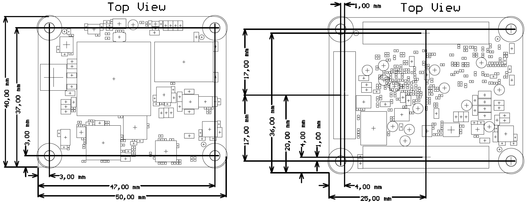
- Dimension
- 40 mm x 50 mm
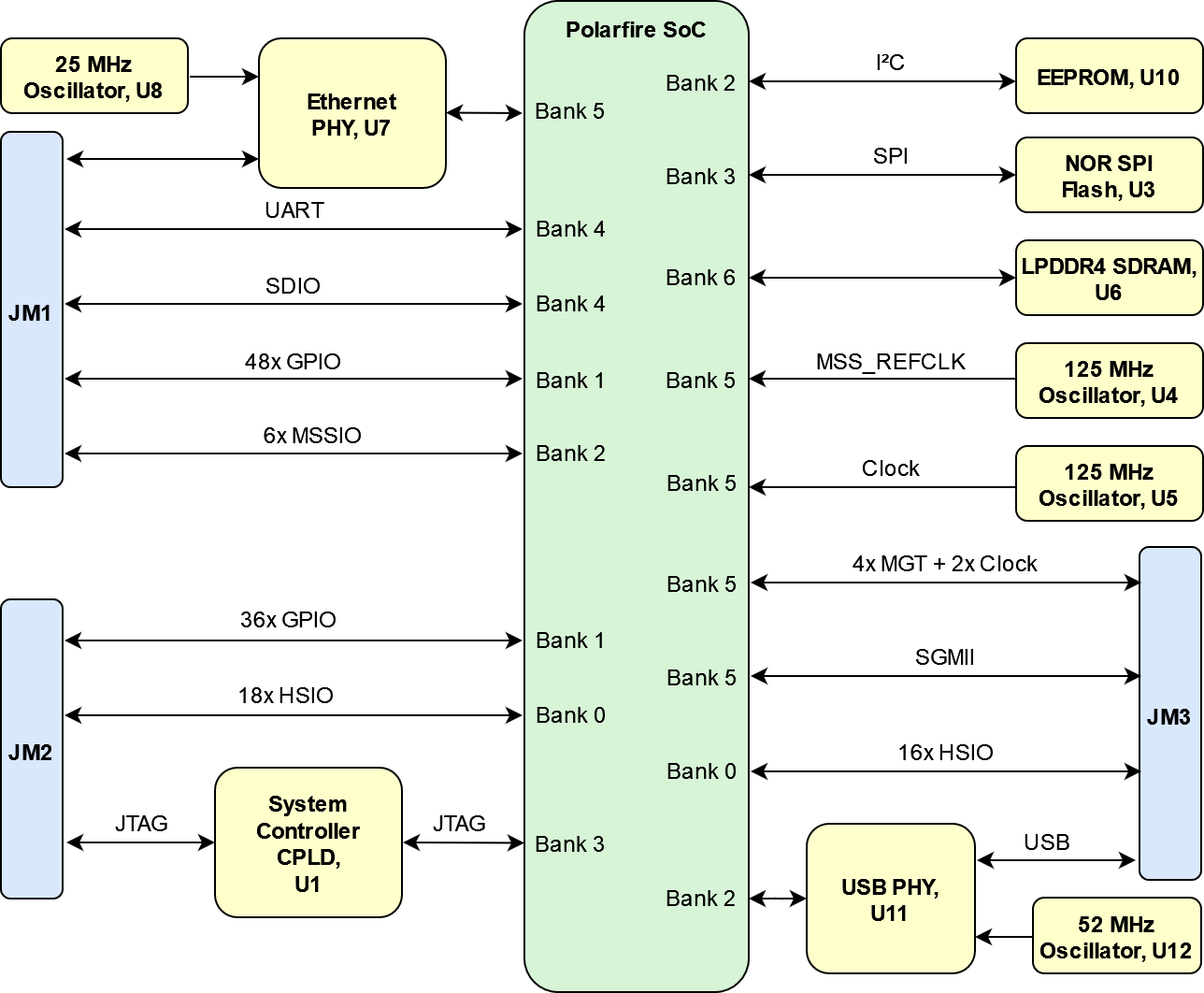
Block Diagram
...
| hidden | true |
|---|---|
| id | Comments |
add drawIO object here.
| Note |
|---|
For more information regarding how to draw a diagram, Please refer to "Diagram Drawing Guidline" . |
...
| anchor | Figure_OV_BD |
|---|---|
| title | TEM0007 block diagram |
...
| Scroll Only |
|---|
|
Main Components
...
| hidden | true |
|---|---|
| id | Comments |
Notes :
- Picture of the PCB (top and bottom side) with labels of important components
- Add List below
| Note |
|---|
For more information regarding how to add board photoes, Please refer to "Diagram Drawing Guidline" . |
...
| anchor | Figure_OV_MC |
|---|---|
| title | TEM0007 main components |
...
| Scroll Only |
|---|
|
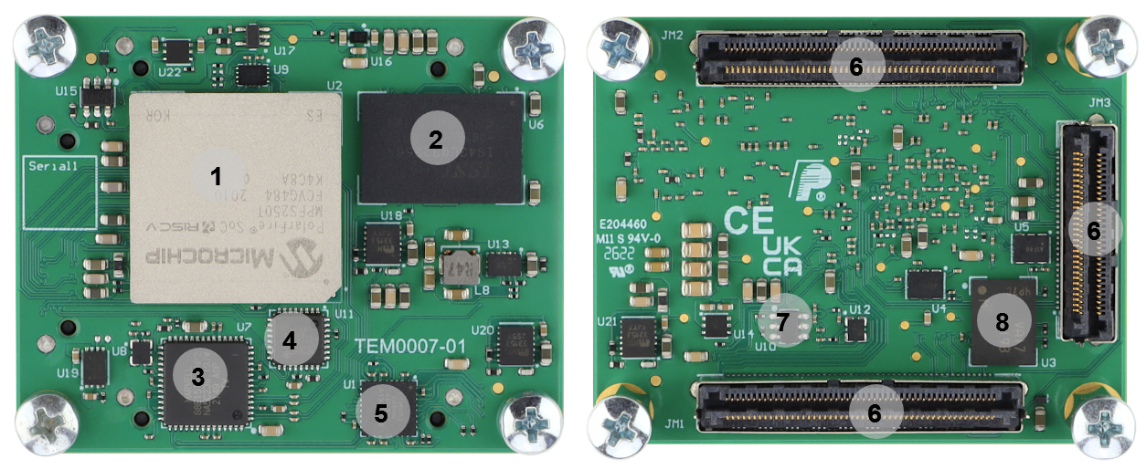
- Microsemi Polarfire SoC MPFS250T, U2
- 1 GByte LPDDR4 SDRAM, U6
- Integrated 10/100/1000 Mbps Energy Efficient Ethernet Transceiver, U7
- Highly Integrated Full Featured Hi-Speed USB 2.0 ULPI Transceiver, U11
- Lattice Semiconductor MachXO2 System Controller CPLD, U1
- B2B Connector Samtec Razor Beam, JM1...3
- EEPROM, U10
- Serial NOR Flash, U3
Initial Delivery State
| Page properties | ||||
|---|---|---|---|---|
| ||||
Notes : Only components like EEPROM, QSPI flash can be initialized by default at manufacture. If there is no components which might have initial data ( possible on carrier) you must keep the table empty |
...
| anchor | Table_OV_IDS |
|---|---|
| title | Initial delivery state of programmable devices on the module |
...
Storage device name
...
Content
...
Notes
...
SPI NOR Flash, U3
...
-
...
-
...
Signals, Interfaces and Pins
| Page properties | ||||
|---|---|---|---|---|
| ||||
Notes :
|
Board to Board (B2B) I/Os
FPGA bank number and number of I/O signals connected to the B2B connector:
...
| anchor | Table_SIP_B2B |
|---|---|
| title | General SoC I/O to B2B connectors information |
...
JTAG Interface
JTAG access to the TEM0007 SoM through B2B connector JM2.
...
| anchor | Table_SIP_JTG |
|---|---|
| title | JTAG pins connection |
...
JTAG Signal
...
B2B Connector
...
JM2-99
...
Pulled Low: Microsemi Polarfire SoC
Pulled High: Lattice MachXO CPLD
UART Interface
The UART interface is connected from the Polarfire SoC to the B2B connector. If this interface is not necessary, these pins can be used for other functionality.
...
| anchor | Table_OBP_UART |
|---|---|
| title | UART interface description |
...
SDIO Interface
The SDIO interface is connected from the Polarfire SoC to the B2B connector. If this interface is not necessary, these pins can be used for other functionality.
...
| anchor | Table_OBP_SDIO |
|---|---|
| title | SDIO interface description |
...
MSSIO Interface
The MSSIO interface is connected from the Polarfire SoC to the B2B connector.
...
| anchor | Table_OBP_MSSIO |
|---|---|
| title | MSSIO interface description |
...
SGMII Interface
The Polarfire Soc provides two SGMII interfaces whereby one interface is connected to the B2B connector.
...
| anchor | Table_OBP_SGMII |
|---|---|
| title | SGMII interface description |
...
MGT Lanes
There are four MGT (Multi Gigabit Transceiver) lanes and two two clocks connected between the B2B connector JM3 and the Polarfire SoC bank 5. Each MGT lane consists of one transmit and one receive (TX/RX) differential pairs, four signals total per one MGT lane. Following table lists lane number, signal schematic name, and board-to-board pin connection:
...
| anchor | Table_SIP_MGT |
|---|---|
| title | MGT Lanes Connection |
...
Lane
...
Schematic
...
Gigabit Ethernet
On-board Gigabit Ethernet PHY (U7) is provided with Marvell Alaska 88E1512 IC. The Ethernet PHY SGMII interface is connected to the Polarfire SoC.
...
| anchor | Table_OBP_ETH |
|---|---|
| title | Gigabit Ethernet pin description |
...
System Controller CPLD I/O Pins
...
SPI_CS , SPI_DQ0... SPI_DQ3
SPI_SCK
...
you must fill the table below with group of MIOs which are connected to a specific components or peripherals, you do not have to specify pins in B2B, Just mention which B2B is connected to MIOs. The rest is clear in the Schematic.
Example:
...
...
Test Points
...
| anchor | Table_OBP_TestPoints |
|---|---|
| title | Test Points Information |
...
On-board Peripherals
...
- 11
...
USB Interface
USB PHY is provided by Microchip USB3320. The ULPI interface is connected to the Polarfire SoC. I/O voltage is fixed at 3.3 V. Reference clock input for the USB PHY is supplied by the on-board 52.00 MHz oscillator (U12).
...
| anchor | Table_OBP_USB |
|---|---|
| title | General Overview of the USB PHY Signals |
...
DP - 18,
...
OTG-D_P
...
...
Notes :
- add subsection for every component which is important for design, for example:
- Two 100 Mbit Ethernet Transciever PHY
- USB PHY
- Programmable Clock Generator
- Oscillators
- eMMCs
- RTC
- FTDI
- ...
- DIP-Switches
- Buttons
- LEDs
| Page properties | ||||
|---|---|---|---|---|
| ||||
Notes : In the on-board peripheral table "chip/Interface" must be linked to the corresponding chapter or subsection |
...
| anchor | Table_OBP |
|---|---|
| title | On board peripherals |
...
System Controller CPLD
The System Controller CPLD (U1) is provided by Lattice Semiconductor LCMXO2-256HC (MachXO2 product family). It is the central system management unit with module specific firmware installed to monitor and control various signals of the FPGA, on-board peripherals, I/O interfaces and module as a whole.
Gigabit Ethernet
On-board Gigabit Ethernet PHY (U7) is provided with Marvell Alaska 88E1512 IC (U7). The Ethernet PHY SGMII interface is connected to the Polarfire SoC. The reference clock input of the PHY is supplied from an on-board 25.00 MHz oscillator (U8).
...
| anchor | Table_OBP_ETH |
|---|---|
| title | Ethernet PHY to Polarfire SoC connections |
...
Bank 5 - N6
...
SGMII0_IN_P
...
U7 - 1
...
Bank 5 - L5
...
SGMII0_OUT_P
...
U7 - 4
...
USB PHY
...
Note: → See examples for different types <Series Name> TRM Template section examples#%3CSeriesName%3ETRMTemplatesectionexamples-KeyFeatures |
| Excerpt |
|---|
|
Block Diagram
| Page properties | ||||||
|---|---|---|---|---|---|---|
| ||||||
add drawIO object in Scroll Ignore section and add reference image in Scroll Only.
|
| Scroll Title | ||||||||||||||||||||||||||||
|---|---|---|---|---|---|---|---|---|---|---|---|---|---|---|---|---|---|---|---|---|---|---|---|---|---|---|---|---|
| ||||||||||||||||||||||||||||
|
Main Components
| Page properties | ||||
|---|---|---|---|---|
| ||||
Notes :
|
| Scroll Title | ||||||||||||||||||||||||||||
|---|---|---|---|---|---|---|---|---|---|---|---|---|---|---|---|---|---|---|---|---|---|---|---|---|---|---|---|---|
| ||||||||||||||||||||||||||||
|
- Microsemi Polarfire SoC, U2
- LPDDR4 SDRAM, U6
- Ethernet Transceiver, U7
- USB Transceiver, U11
- System Controller CPLD, U1
- B2B Connector, JM1, JM2, JM3
- EEPROM, U10
- Serial NOR Flash, U3
Initial Delivery State
| Page properties | ||||
|---|---|---|---|---|
| ||||
|
| Scroll Title | ||
|---|---|---|
|
...
...
U2 - G4
...
OTG-STP
...
U11 - 29
...
U2 - F1
...
OTG-DIR
...
U11 - 31
...
OTG_DATA0
...
LPDDR4 SDRAM
| Page properties | ||||
|---|---|---|---|---|
| ||||
Notes : Minimum and Maximum density of DDR3 SDRAM must be mentioned for other assembly options. (pay attention to supported address length for DDR3) |
The TEM0007 SoM has a one GByte volatile LPDDR4 SDRAM IC for storing user application code and data.
- Part number: IS43LQ32256A-062BLI
- Supply voltage: +1.8 V / +1.1 V
- Speed: 1600 MHz
- Temperature: Industrial (-40°C to +85°C)
EEPROM
There is a 2 Kbit EEPROM provided on the module TEM0007 with a pre-programmed globally unique MAC.
...
| anchor | Table_OBP_EEP |
|---|---|
| title | I2C EEPROM interface MSSIOs and pins |
...
...
...
...
SPI Flash Memory
| Page properties | ||||
|---|---|---|---|---|
| ||||
Notes : Minimum and Maximum density of quad SPI flash must be mentioned for other assembly options. |
The TEM0007 is equipped with a MT25QU512ABB8E12-0SIT flash memory chip, U3, which provided storage for FPGA configuration files. After configuration, the remaining free memory can be used for application data storage.
...
| anchor | Table_OBP_SPI |
|---|---|
| title | SPI Flash interface pins |
...
...
...
...
...
Power and Power-On Sequence
...
| hidden | true |
|---|---|
| id | Comments |
In 'Power and Power-on Sequence' section there are three important digrams which must be drawn:
- Power on-sequence
- Power distribution
- Voltage monitoring circuit
| Note |
|---|
For more information regarding how to draw diagram, Please refer to "Diagram Drawing Guidline" . |
Power Supply
Power supply with minimum current capability of 3 A for system startup is recommended.
Power Consumption
...
| anchor | Table_PWR_PC |
|---|---|
| title | Power Consumption |
...
* TBD - To Be Determined
Power Distribution Dependencies
...
| anchor | Figure_PWR_PD |
|---|---|
| title | Power Distribution |
...
| Scroll Only |
|---|
|

Power-On Sequence
The power sequence is the recommended one. The final sequence depends on the system controller.
...
| anchor | Figure_PWR_PS |
|---|---|
| title | Power Sequency |
...
| Scroll Only |
|---|
|

Voltage Monitor Circuit
The TEM0007 delivers two voltage monitor circuits. The first circuit is responsible for the selection of voltage "VDDAUX1". This voltage is selected on the basis of the voltage of "VCCIOB". If "VCCIOB" is higher than 2.9 V, "VDDAUX1" should be +3.3 V. If it is smaller, "VDDAX1" should be +2.5 V. The second circuit monitors the +1.0 V power rail. According to this rail, the reset is set/unset to realize a brown-out detection. Furthermore, a possibility for a manual reset is available.
...
| anchor | Figure_PWR_VMC |
|---|---|
| title | Voltage Monitor Circuit |
...
| Scroll Only |
|---|
|

...
...
...
...
B2B Connector
JM2 Pin
...
...
...
...
...
...
...
...
...
...
...
...
...
...
...
...
Bank
...
Voltage
...
VCCIOB
...
...
...
...
...
...
...
...
...
...
...
...
VCCIOB
...
Recommended Operating Conditions
...
...
...
...
...
...
...
...
...
...
...
...
...
...
|
Currently Offered Variants
| Page properties | ||||
|---|---|---|---|---|
| ||||
Set correct link to the shop page overview table of the product on English and German. Example for |
...
...
...
...
...
...
...
...
...
...
...
Revision History
Hardware Revision History
...
| hidden | true |
|---|---|
| id | Comments |
Set correct links to download arrier, e.g. TE0706 REV02:
TE0706-02 -> https://shop.trenz-electronic.de/Download/?path=Trenz_Electronic/Modules_and_Module_Carriers/4x5/4x5_Carriers/TE0706/REV02/Documents
Note:
| ||||||||||||||||||||||||||||
|

...
...
...
...
Overview
Content Tools