Page History
| Scroll Ignore |
|---|
Download PDF Version version of this Documentdocument. |
| Scroll pdf ignore | |||
|---|---|---|---|
Table of Contents
|
Overview
| Scroll Only (inline) |
|---|
...
Refer to https:// |
...
wiki.trenz-electronic.de/display/PD/TE0710+TRM for online version of this manual and the rest of available documentation. |
Trenz Electronic de/Download/?path=Trenz_Electronic/TE0710 Trenz Electronic TE0710 is an industrial-grade FPGA module integrating a Xilinx Artix-7 FPGA, Dual two 10/100 MBit Mbit Ethernet PHYs, 512 MByte DDR3 SDRAM with 8-bit data-width, 32 MByte Quad SPI Flash memory for configuration and operation and powerful switchswitching-mode power supplies for all on-board voltages. A large number of Numerous configurable I/O's is Os are provided via rugged high-speed stacking strips. All modules in 4 x 5 cm form factor are mechanically compatible.
...
this on a tiny footprint, smaller than a credit card
...
size at
...
very competitive price. All Trenz Electronic SoMs in 4 x 5 cm form factor are mechanically compatible.
Block Diagram
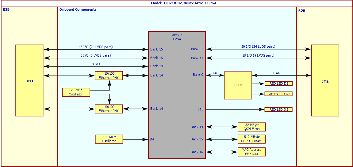
Figure 1: TE0710-02 Block Diagram
Main Components
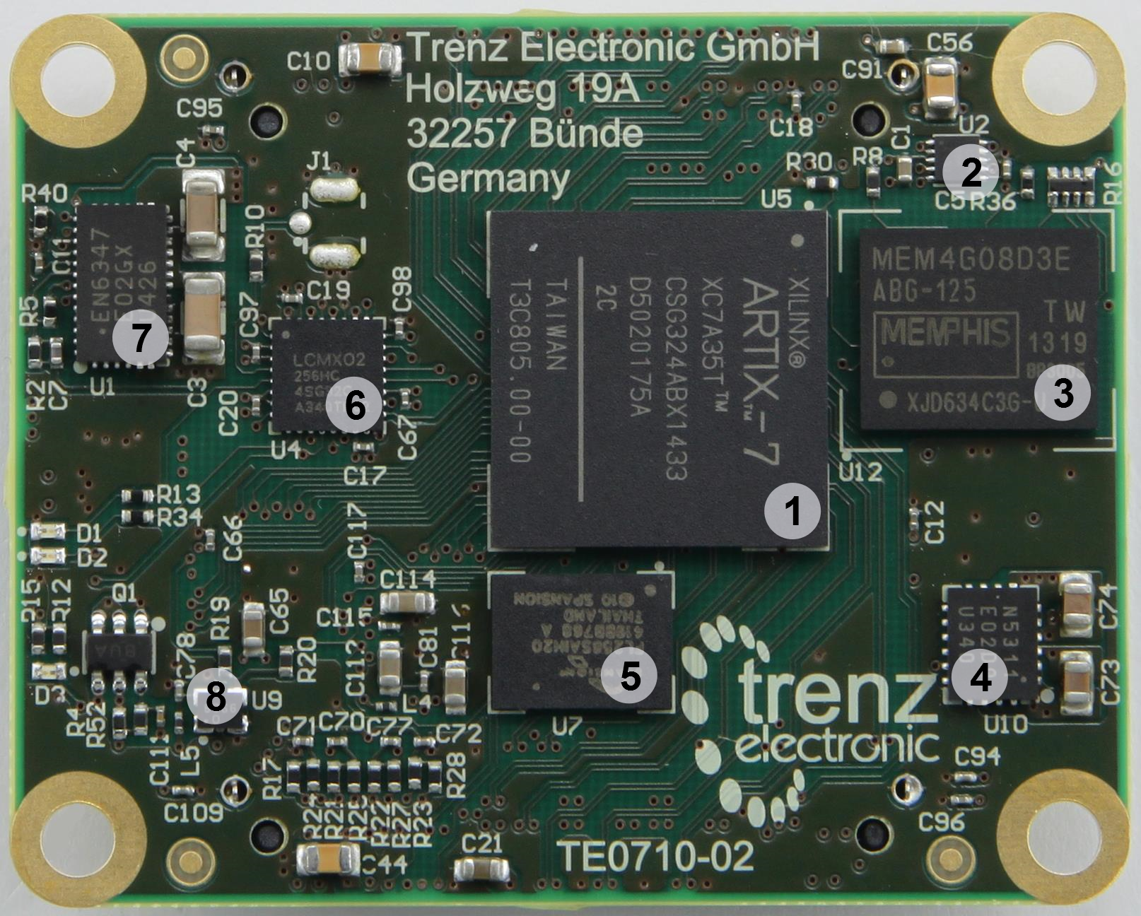
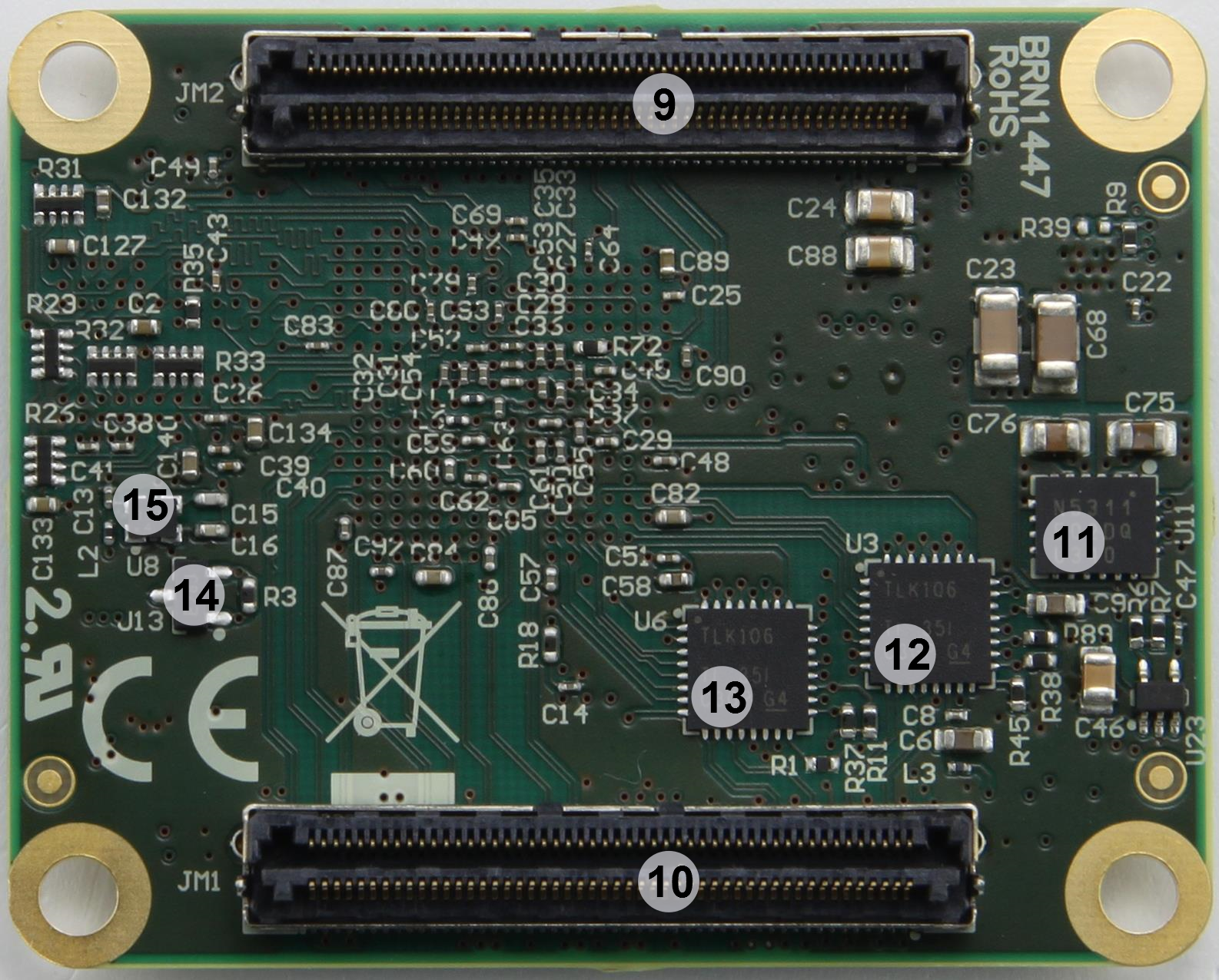
Figure 2: TE0710 (REV 02).
- Artix-7 (15T to 100T) FPGA
- TPS51206 DDR3-SDRAM voltage supply
- MEM4G08D3EABG 512 MByte DDR3 SDRAM
- EN5311QI Voltage Regulator 1.5V
- S25FL256S 32 Mbyte Quad SPI Flash memory
- System Controller CPLD (Lattice LCMXO2-256HC): 256 Macrocell CPLD
- EN6347QI voltage Regulator 1.0V
- SiT8008AI 25 MHz Ethernet reference clock
- B2B connector JM2 (0,40 mm Razor Beam™ High Speed Hermaphroditic Terminal/Socket Strip (LSHM-150))
- B2B connector JM1 (0,40 mm Razor Beam™ High Speed Hermaphroditic Terminal/Socket Strip (LSHM-150))
- EN5311QI voltage Regulator 1.8V
- TLK106 10/100 Mbps Ethernet PHY
- TLK106 10/100 Mbps Ethernet PHY
- 11AA02E48T-I/TT 2 Kbit EEPROM with UNI/O serial interface
- SiT8008AI 100 MHz reference clock (connected to FPGA bank 35)
Key Features
Industrial-grade Xilinx Artix-7 (15T to 100T) SoM (System on Module), supported by the free Xilinx Vivado WebPACK tool
Rugged for shock and high vibration
512 MByte DDR3 SDRAM
Dual 10/100 MBit Ethernet PHY
MAC Address EEPROM
32 MByte QSPI Flash memory (with XiP support)
100 MHz MEMS oscillator
Plug-on module with 2 × 100-pin high-speed hermaphroditic strips
112 FPGA I/Os (51 differential pairs) are available on board-to-board connectors
On-board high-efficiency DC-DC converters
4.0 A x 1.0 V power rail
1.0 A x 1.8 V power rail
1.0 A x 1.5 V power rail
System management and power sequencing
eFUSE bit-stream encryption
AES bit-stream encryption
User LED
Evenly-spread supply pins for good signal integrity
Assembly options for cost or performance optimization available upon request.
Initial Delivery State
...
Content
...
Notes
...
SPI Flash OTP Area
...
Empty, not programmed
...
Except serial number programmed by flash vendor.
...
SPI Flash Quad Enable bit
...
Programmed
...
SPI Flash main array
...
Demo design
...
EFUSE USER
...
Not programmed
...
EFUSE Security
...
Not programmed
...
Table 1: Initial delivery state
Signals, Interfaces and Pins
Board to Board (B2B) I/Os
I/O signals connected to the FPGA's I/O banks and B2B connector:
...
0
...
HR
...
-
...
-
...
14
...
HR
...
JM1
...
8 I/O-pins
...
3.3V
...
HR-Banks support voltages from 1.2V to 3.3V standards.
See the Artix-7 datasheet (DS181) for the allowable voltage range.
...
15
...
HR
...
JM1
...
48 I/O-pins
24 LVDS-pairs possible
...
user
...
16
...
HR
...
JM1
...
6 I/O-pins
3 LVDS-pairs possible
...
3.3V
...
50 I/O-pins
24 LVDS-pairs possible
...
Table 2: Voltage ranges and pin-outs of available logic banks of the FPGA
Please use Master Pinout Table table as primary reference for the pin mapping information.
JTAG Interface
JTAG access to the Xilinx Artix-7 and to the System Controller CPLD is provided through B2B connector JM2.
...
JM2-93
...
Table 3: Pin-mapping of JTAG Interface on B2B connector
| Note |
|---|
Select by JTAGEN pin on B2B connector JM1-89 either to access FPGA Artix-7 (JTAGEN pin driven low or open) or System Controller via JTAG (JTAGEN pin driven high). The use of Xilinx legacy development tools (ISE, Impact) is not recommended. Impact recognizes only A100T, any smaller Artix-7 FPGA is not recognized as Xilinx FPGA by Impact. |
System Controller I/O Pins
Special purpose pins are connected to smaller System Controller CPLD and have following default configuration:
...
Table 4: Pin-description of System Controller CPLD
LEDs
On the SoM TE0710 there is a total of 3 LEDS available. Two LEDs are status LEDs, one can freely used in costumer designs. The user LED is routed to the FPGA by the net with the schematic-name 'USERLED'.
When the FPGA is not configured the status LEDs will flash continuously. Finally once FPGA configuration has completed the status LEDs can be used in the user's FPGA design.
...
Table 5: Description of the on board LEDs
Clocking
The TE0710 is equipped with two Sitara reference clocks to provide clock signals to the Ethernet PHYs and for the on board 512 MByte DDR3 SRRAM.
...
Ethernet reference
...
25 MHz
...
U8 SiT8008AI-73-XXS-100.000000E
...
Key Features
Industrial-grade Xilinx Artix-7 FPGA (15T to 100T) , supported by the free Xilinx Vivado WebPACK development tool
Rugged for shock and high vibration
512 MByte DDR3 SDRAM
Dual 10/100 Mbit Ethernet PHY
MAC Address EEPROM
32 MByte QSPI Flash memory (with XiP support)
100 MHz MEMS oscillator
Plug-on module with 2 × 100-pin high-speed hermaphroditic strips
112 FPGA I/Os (51 differential pairs) are available via board-to-board connectors
On-board high-efficiency DC-DC converters
4.0 A x 1.0 V power rail
1.0 A x 1.8 V power rail
1.0 A x 1.5 V power rail
System management and power sequencing
eFUSE bit-stream encryption
AES bit-stream encryption
User LED
Evenly-spread supply pins for good signal integrity
NB! Assembly options for cost or performance optimization are available upon request.
Block Diagram
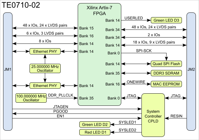
Figure 1: TE0710-02 block diagram.
| Page break |
|---|
Main Components
Figure 2: TE0710-02 PCB.
- Xilinx Artix-7 FPGA , U5
- Voltage regulator for DDR3 SDRAM (Texas Instruments TPS51206), U2
- 512 MByte DDR3 SDRAM (Memphis MEM4G08D3EABG), U12
- 1A PowerSoC DC-DC converter for 1.5V (Altera EN5311QI), U10
- 32 MByte Quad SPI Flash memory (Cypress S25FL256S), U7
- System Controller CPLD (Lattice Semiconductor LCMXO2-256HC), U4
- 4A PowerSoC DC-DC converter for 1.0V (Altera EN6347QI), U1
- Programmable oscillator @25.000000 MHz for Ethernet reference clock (SiTime SiT8008), U9
- B2B connector (0,40 mm Razor Beam™ High Speed Hermaphroditic Strip LSHM-150), JM2
- B2B connector (0,40 mm Razor Beam™ High Speed Hermaphroditic Strip LSHM-150), JM1
- 1A PowerSoC DC-DC converter for 1.5V for 1.8V (Altera EN5311QI), U11
- 10/100 Mbps Ethernet PHY (Texas Instruments TLK106), U3
- 10/100 Mbps Ethernet PHY (Texas Instruments TLK106), U6
- 2 Kbit serial EEPROM with UNI/O serial interface (Microchip 11AA02E48T-I/TT), U13
- Programmable oscillator @100.000000 MHz for reference clock (SiTime SiT8008), U8
| Page break |
|---|
Initial Delivery State
| Storage Component | Content | Notes |
|---|---|---|
SPI Flash OTP Area | Empty, not programmed | Except serial number programmed by flash vendor. |
SPI Flash Quad Enable bit | Programmed | - |
SPI Flash main arraay | Empty | - |
eFUSE USER | Not programmed | - |
eFUSE Security | Not programmed | - |
Table 1: TE0710-02 module initial delivery state.
Signals, Interfaces and Pins
Board to Board (B2B) I/Os
FPGAs I/O banks, voltages and B2B connections:
| Bank | Type | B2B Connector | I/O Signal Count | Voltage | Notes |
|---|---|---|---|---|---|
14 | HR | JM1 | 8 I/O pins | 3.3V | HR banks support voltages from 1.2V to 3.3V. See Xilinx Artix-7 datasheet (DS181) for voltage ranges. |
15 | HR | JM1 | 48 I/O pins 24 LVDS pairs | User | Same as above. |
16 | HR | JM1 | 6 I/O pins 3 LVDS pairs | 3.3V | Same as above. |
| 34 | HR | JM2 | 50 I/O pins 24 LVDS pairs | User | Same as above. |
Table 2: FPGA I/O banks.
Please refer to Pin-out tables page for more information.
Page break
JTAG Interface
JTAG access to the Xilinx Artix-7 and System Controller CPLD is provided through B2B connector JM2.
| JTAG Signal | B2B Pin |
|---|---|
| TMS | JM2-93 |
| TDI | JM2-95 |
| TDO | JM2-97 |
| TCK | JM2-99 |
Table 3: JTAG interface connector.
| Note |
|---|
JTAGEN pin on B2B connector JM1 is used to control which physical device is accessible via JTAG interface. If this pin is set to low or left open, JTAG interface is enabled for Xilinx Artix-7 FPGA, if set to high, JTAG interface for System Controller CPLD will be enabled. The use of Xilinx legacy development tools (ISE, iMPACT) is not recommended. iMPACT does not recognize any Xilinx Artix-7 below A100T model. |
System Controller I/O Pins
Special purpose pins are connected to the System Controller CPLD which have following default function:
| Pin Name | Mode | Function | Default Configuration | B2B Pin |
|---|---|---|---|---|
| PGOOD | Output | Power Good | Active high when all on-module power supplies are operating properly. | JM1-30 |
| RESIN | Input | Reset | Active low, drive low to keep system in reset state (FPGA pin PROG_B will be driven by CPLD). | JM2-18 |
| EN1 | Input | Reset | Same as RESIN, can be left unconnected. | JM1-28 |
| JTAGEN | Input | JTAG Select | Low for normal operation, high (3.3V) to enable JTAG for System Controller CPLD. | JM1-89 |
| MODE | - | - | Not used by default, leave open. | JM1-32 |
| NOSEQ | - | - | Not used by default, leave open. | JM1-7 |
Table 4: Special purpose pins description of the System Controller CPLD.
| Page break |
|---|
On-board LEDs
There are three LEDs available on TE0710-02 SoM. Two are status LEDs, and one can be freely used by user design. The user LED is routed to the FPGA as 'USERLED'.
When the FPGA is not configured the status LEDs will flash continuously. Once the FPGA configuration has completed, the status LEDs can be used by the user FPGA design.
| LED | Color | Connected to | Description and Notes |
|---|---|---|---|
| D1 | Red | SYSLED2 | System Controller status LED, connected to CPLD. |
| D2 | Green | SYSLED1 | System Controller status LED, connected to CPLD. |
| D3 | Red | USERLED | User LED, active LOW, connected to FPGA pin L15. |
Table 5: On-board LEDs.
Clocking
The TE0710-02 SoM is equipped with two MEMS oscillators to provide clock signals for two on-board Ethernet PHYs and DDR3 SDRAM.
| Clock | Frequency | IC | Connected to | Notes |
|---|---|---|---|---|
Ethernet reference | 25 MHz | U9, SiT8008AI-73-XXS-25.000000E | ICs U3, U6 TLK106RHB | Clock signal shared by both Ethernet PHYs. |
| DDR3 SDRAM reference | 100 MHz | U8, SiT8008AI-73-XXS-100.000000E | FPGA bank 35, pin F4 | Differential clock signal for DDR3 SDRAM IC, U12. |
Table 6: Clocks overview.
On-board Peripherals
32 MByte Quad SPI Flash Memory
An SPI flash memory S25FL256S (U7) is provided for FPGA configuration file storage. After configuration completes the remaining free memory can be used for application data storage. All four SPI data lines are connected to the FPGA allowing x1, x2 or x4 data bus widths. Maximum data rate depends on the selected bus width and clock frequency used.
| Note |
|---|
SPI Flash QE (Quad Enable) bit must be set to high or FPGA is unable to load its configuration from flash during power-on. By default this bit is set to high at the manufacturing plant. |
System Controller CPLD
System Controller CPLD (Lattice MachXO2-256HC, U4) is used to control FPGA configuration process. The FPGA is held in reset (by driving the PROG_B signal low) until all power supplies have stabilized.
By driving signal RESIN to low you can reset the FPGA. This signal can be driven from the user’s baseboard PCB via the B2B connector JM2 pin 18.
Input EN1 is also gated to FPGA reset, should be open or pulled up for normal operation. By driving EN1 low, on-board DC-DC converters are not turned off.
User can create their own System Controller design using Lattice Diamond software. Once created it can be programmed into CPLD via JTAG interface.
| Page break |
|---|
DDR3 SDRAM
The TE0710-02 SoM has one 512 MByte volatile DDR3 SDRAM IC (U12) for storing user code and data.
- Part number: MEM4G08D3EABG-125 (Memphis)
- Supply voltage: 1.5V
- Organization: 64M words x 8 bits x 8 banks
- Memory speed limited by Xilinx Artix-7 speed grade and MIG
Configuration of the DDR3 memory controller in the FPGA should be done using the MIG tool in the Xilinx Vivado Design Suite IP catalog.
Ethernet PHYs
The TE0710-02 is equipped with two Texas Instruments TLK106 10/100 Mbit Ethernet PHYs (U3 and U6). The I/O voltage is fixed at 3.3V. The reference clock input for both PHYs is supplied by on-board 25 MHz oscillator (U9). Both Ethernet PHYs are connected to FPGA bank 14 using MII interface.
Note: Pin ETH2_INT (power down or interrupt, default function is power down) is connected to FPGA bank 16 (pin D10).
MAC Address EEPROM
TE0710-02 module is equipped with 2 Kbit serial Electrically Erasable PROM (EEPROM, U14). It provides pre-programmed 48-bit Extended Unique Identifier (EUI-48™) to identify network hardware MAC address which is write-protected to ensure tamper-proof designs. This EEPROM can be accessed by UNI/O® serial interface bus using Manchester encoding techniques. The clock and data are combined into a single, serial bit stream (SCIO), where the clock signal is extracted by the receiver to correctly decode the timing and value of each bit. The bus is controlled by a master device (Xilinx Artix-7) which determines the clock period, controls the bus access and initiates all operations, while the EEPROM works as a slave. Refer to Microchip's 11AA02E48 datasheet for more information
Table 6: Clocks overview
Onboard Peripherals
32 Mbyte Quad SPI Flash Memory
An SPI flash memory S25FL256S (U7) is provided for FPGA configuration file storage. After configuration completes the remaining free memory can be used for application data storage. All four SPI data lines are connected to the FPGA allowing x1, x2 or x4 data bus widths to be used. The maximum data rate will be dependent on the bus width and clock frequency.
| Note |
|---|
SPI Flash QE (Quad Enable) bit must be set, or the FPGA would not configure from Flash. This bit is always set at manufacturing. |
System Controller
The system controller is used to coordinate the configuration of the FPGA. The FPGA is held in reset (by driving the PROG_B signal) until the power supplies have sequenced. Low level at RESIN pin also resets the FPGA. This signal can be driven from the user’s PCB via the B2B connector pin JM2-18. Input EN1 is also gated to FPGA Reset, should be open or pulled up for normal operation. EN1 low does not turn off on board DCDC converters.
It is possible for the user to create their own system controller design using the Lattice Diamond software. Once created the design can be programmed into the device using the JTAG pins. The signal JTAGEN should be set to 3.3V to enable programming mode. For normal operation it should be set to 0V.
There are two LEDs that are connected to the system controller. When the FPGA is not configured the LEDs will flash continuously. Finally once FPGA configuration has completed the LEDs can be used in the user's FPGA design.
DDR3 SDRAM
The TE0710-02 board is equipped with one DDR3 SRRAM IC (U12) with a capacity of 512 MByte volatile memory for storing user code and data.
- Part number: MEM4G08D3EABG-125 (Memphis)
- Supply voltage: 1.5V
- Organization: 64M words x 8 bits x 8 banks
- Memory speed limited by Artix speed grade and MIG
Configuration of the DDR3 memory controller in the FPGA should be done using the Xilinx MIG tool in the Vivado IP catalog.
Ethernet
The TE0710-02 is equipped with two TI TLK106 10/100 MBit Ethernet PHYs (U3 and U6). The I/O Voltage is fixed at 3.3V. The reference clock input for both PHYs is supplied from an on board 25MHz oscillator (U9).
Both Ethernet PHYs are connected to FPGA Bank 14 using MII interface.
Note: Pin ETH2_INT (power down or interrupt, default function is power down) is connected to FPGA bank 16 (pin D10).
Power and Power-On Sequence
...
| Power Input Pin | Voltage Range | Max Current |
|---|---|---|
| VIN | 3.3V to 5.5V | Typical 200mA, depending depends on customer design and connectionssetup. |
| 3.3VIN | 3.3V | Typical 50mA, depending depends on customer design and connectionssetup. |
Table 7: maximal current of power suppliesTypical power consumption during normal operation.
| Tip |
|---|
Vin VIN and Vin 3.3V 3VIN can be connected to the same power source (3.3 V). |
Lowest power consumption is achieved when powering the module from single 3.3V power supply. When using split 3.3V/5V supplies the power consumption (and heat dissipation) will rise, this is due to the DC/-DC converter efficiency (it decreases when VIN/VOUT ratio rises).
...
For highest efficiency of on-board DC/-DC regulators, it is recommended to use same 3.3V power source for both VIN and 3.3VIN power rails. Although VIN and 3.3VIN can be powered up in any order, it is recommended to power them up simultaneously.
It is important that all baseboard I/O's Os are 3-stated at power-on until System Controller sets PGOOD signal high (B2B connector JM1, pin 30), or 3.3V is present on B2B connector JM2 pins 10,12 or 91, meaning that all on-module voltages have become stable and module is properly powered up.
See Xilinx datasheet DS181 (for Artix7) for additional information. User should also check related baseboard documentation when choosing baseboard design for TE0710-02 module.
A 3.3V supply is also needed and must be supplied from the user's PCB. An output 3.3V supply is available on some of the board connector pins (see section 'Power Rails'). The input 3.3VIN will be switched to the internal 3.3V voltage level after the FPGA 1.0V supply is stable. Than 3.3V supply will be available on the B2B connector pins.
...
- Apply 5V to pins VIN and 3.3V to pins 3.3VIN on the board connector
- Apply 3.3V to pins VIN and 3.3VIN on the board connectors.
Power Rails and Bank Voltages
Voltages on B2B- Connectors | B2B JM1-Pin | B2B JM2-Pin | Direction | Note | ||||
|---|---|---|---|---|---|---|---|---|
| VIN | 1, 3, 5 | 2, 4, 6, 8 | inputInput | supply Supply voltage | ||||
| 3.3VIN | 13, 15 | - | inputInput | supply Supply voltage | ||||
| VCCIO15 | 9, 11 | - | inputInput | high High range bank voltage | ||||
| VCCIO34 | - | 7, 9 | inputInput | high High range bank voltage | ||||
| 3.3V | - | 10, 12 | Output | 3.3V | 14 | 10, 12, 91 | output | Internal 3.3V voltage level |
| JTAG VREF | - | 91 | Output | JTAG reference voltage (3.3V).internal 3.3V voltage level | ||||
| 1.8V | 39 | - | outputOutput | internal Internal 1.8V voltage level | ||||
| 1.5V | - | 19 | outputOutput | internal Internal 1.5V voltage level |
Table 8: Power rails of SoM on B2B connectors.
| FPGA Bank |
|---|
...
| Bank | Schematic Schematics Name | Voltage | Range | |
|---|---|---|---|---|
| 0 Config | 3.3V | 3.3V | - | |
| 14 | 3.3V | 3.3V | - | |
| 15 | VCCIO15 | userUser | HR: 1.2V to 3.3V | |
| 16 | 3.3V | 3.3V | - | |
| 34 | VCCIO34 | userUser | HR: 1.2V to 3.3V | |
| 35 | 1.5V | 1.5V | - |
Table 9: Range of FPGA 's bank voltages.
See the Artix7 Xilinx Artix-7 datasheet DS181 for the allowable allowed voltage rangeranges.
Board to Board Connectors
| Include Page | ||||||
|---|---|---|---|---|---|---|
|
Variants Currently In Production
Module Variant | FPGA | FPGA Junction Temperature | Operating Temperature Range | TE0710-02-100-2CF | XC7A100T-2CSG324C | 0°C to 85°C | commercial grade|
|---|---|---|---|---|---|---|---|
| TE0710-02-35- | 2CF2IF | XC7A35T- | 2CSG324C2CSG324I | 0°C -40°C to 85°C100°C | commercial Industrial grade | ||
| TE0710-02-100-2IF | XC7A100T-2CSG324I | -40°C to 100°C | industrial Industrial grade | TE0710||||
| TE0710-02-35- | 2IF2CF | XC7A35T- | 2CSG324I2CSG324C | -40°C 0°C to 100°C85°C | industrial Commercial grade | ||
| TE0710-02-100-1Q2CF | XA7A100TXC7A100T-1CSG324Q2CSG324C | -40°C 0°C to 125°C85°C | industrial Commercial grade |
Table 10: Differences between variants of Module TE0710-02 variants.
Technical Specifications
Absolute Maximum Ratings
| Parameter | Min | Max | Units | Notes |
|---|---|---|---|---|
VIN supply voltage | -0.3 | 7.0 | V | EN6347QI |
| , EN5311QI |
| datasheet | ||||
| 3.3VIN supply voltage | -0.1 | 3.6 | V | - |
| HR I/O |
| banks supply voltage (VCCO) | -0.5 | 3.6 | V |
| Xilinx datasheet DS181 | |
| HR I/O banks input voltage | -0.4 |
| VCCO |
| + 0.55 | V |
| Xilinx datasheet DS181 |
| Voltage on module JTAG pins | -0.5 |
| VCCO_0 + 0.45 | V | VCCO_0 is 3.3V nominal |
| Storage temperature | -55 | +100 | °C | - |
Table 11: Absolute maximum ratings.
Recommended
...
Operating Conditions
| Parameter | Min | Max | Units | Notes |
|---|
| VIN supply voltage | 2.4 | 5.5 | V |
| EN5311QI data sheet |
| 3.3VIN supply voltage | 3.135 | 3.465 | V |
3,3V ± 5% |
| HR I/O |
| banks supply voltage |
| (VCCO) | 1.14 | 3.465 | V |
Xilinx datasheet DS181 |
| HR I/O |
Xilinx datasheet DS181
Table 12: Recommended operation conditions
| banks input voltage | -0.20 | VCCO + 0.2 | V | Xilinx datasheet DS181 |
| Voltage on JTAG pins | 3.135 | 3.465 | V | 3,3V ± 5% |
Table 12: Recommended operating conditions.
Operating Temperature Ranges
Commercial grade: 0°C to +70°C.
Industrial: -40°C to +85°C.
Operating temperature range depends also on customer design and cooling solution. Please contact Trenz Electronic for options.
| Note |
|---|
| Please check Xilinx datasheet DS181 |
| Note |
| Please check Xilinx datasheet (DS181) for complete list of absolute maximum and recommended operating ratings. |
Operating Temperature Ranges
Commercial grade: 0°C to +70°C.
Industrial grade: -40°C to +85°C.
The module operating temperature range depends also on customer design and cooling solution. Please contact us for options.
Physical Dimensions
- Module size: 50 mm × 40 mm. Please download the assembly diagram for exact numbers.
- Mating height with standard connectors: 8mm
- PCB thickness: 1.6mm
- Highest part on PCB: approx. 2.5mm. Please download the step model for exact numbers.
All dimensions are shown in mm.
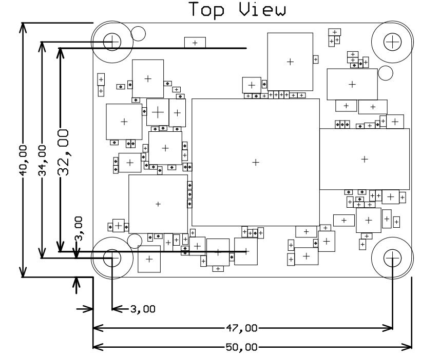
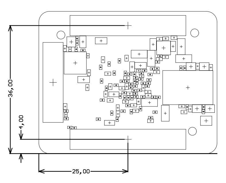
Figure 3: Physical Dimensions of the TE0710-02 board
Weight
...
| operating ratings. |
| Page break |
|---|
Physical Dimensions
- Module size: 50 mm × 40 mm. Please download the assembly diagram for exact numbers.
- Mating height with standard connectors: 8mm
- PCB thickness: 1.4mm+/-10%
- Highest part on PCB: approx. 2.5mm. Please download the step model for exact numbers.
All dimensions are shown in millimeters.
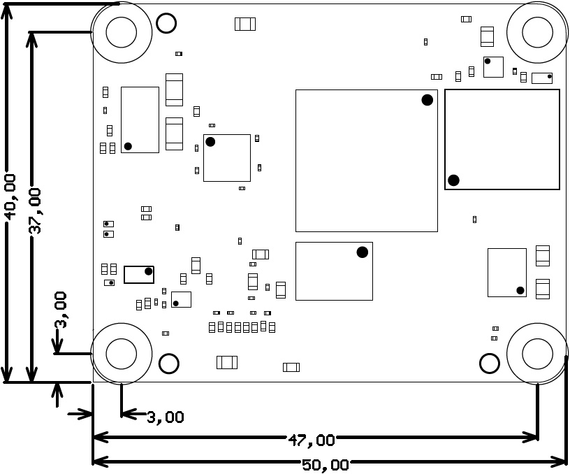
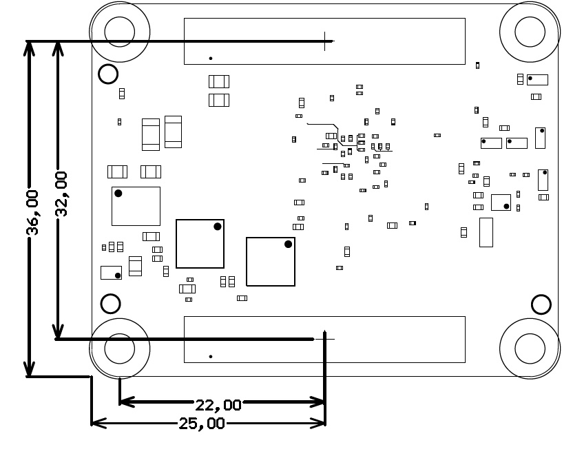
Figure 3: Physical dimensions of the TE0710-02 SoM.
Revision History
Hardware Revision History
| Date | Revision | Notes | PCN | Documentation Link |
|---|---|---|---|---|
| 2014-03-07 | 02 | Current hardware version | TE0710-02 | |
| 01 | First production release |
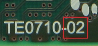
Hardware revision number is printed on the PCB board together with the module model number separated by the dash.
Document Change History
| Date | Revision | Contributors | Description | ||||||||||||||||||||||
|---|---|---|---|---|---|---|---|---|---|---|---|---|---|---|---|---|---|---|---|---|---|---|---|---|---|
|
|
|
| ||||||||||||||||||||||
| 2018-04-20 | v.9 | John Hartfiel |
| ||||||||||||||||||||||
| 2017-11-10 | v.5 | John Hartfiel |
| ||||||||||||||||||||||
| 2017-01-26 | v.4 | Jan Kumann |
| ||||||||||||||||||||||
| 2017-01-24 | v.3 | Jan Kumann |
| ||||||||||||||||||||||
| 2017-01-01 | v.2 | Jan Kumann |
|
Revision History
Hardware Revision History
...
Hardware revision number is printed on the PCB board together with the module model number separated by the dash.
Document Change History
| Date | Revision | Contributors | Description | |||||||
|---|---|---|---|---|---|---|---|---|---|---|
| 2016-12-19 | Ali Naseri | TRM revision | ||||||||
| 2015-01-23 | 0v.1 | initial version
|
|
Disclaimer
| Include Page | ||||
|---|---|---|---|---|
|
Overview
Content Tools