Page History
Template Revision 2.12
...
...
...
Table of Contents
| Table of Contents |
|---|
...
...
...
...
...
| Page properties | ||||
|---|---|---|---|---|
| ||||
Notes :
|
...
...
...
...
Key Features' must be split into 6 main groups for modues:
- SoC/FPGA
- Package:
- Speed:
- Temperature:
- RAM/Storage
- E.g. SDRAM, SPI
- On Board
- E.g. CPLD, PLL
- Interface
- E.g. ETH, USB, B2B, Display port
- Power
- E.g. Input supply voltage
- Dimension
Key Features' must be split into 6 main groups for carrier:
...
- TE0808, TE807, TE0803,...
...
- E.g. SDRAM, SPI
...
- E.g. CPLD, PLL
...
- E.g. ETH, USB, B2B, Display port
...
- E.g. Input supply voltage
...
...
...
...
...
...
...
...
|
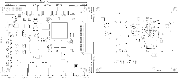
Main Components
| Page properties | ||||
|---|---|---|---|---|
| ||||
Notes :
|
| Scroll Title | |||||
|---|---|---|---|---|---|
| |||||
|
...
...
...
|
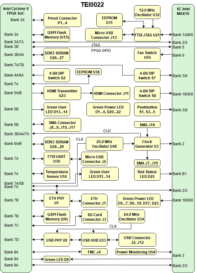
- Intel Cyclone V, U10
- DDR3 SDRAM, U26...27
- DDR3 SDRAM, U28...29
- FMC, J4
...
...
...
...
...
...
...
...
00
...
...
...
...
...
...
...
...
...
...
...
...
...
...
...
...
| Page properties | ||||
|---|---|---|---|---|
| ||||
Notes :
|
...
...
...
...
...
...
...
...
...
...
...
...
...
...
...
...
...
...
...
...
...
...
...
...
...
...
...
...
...
...
...
...
...
...
...
...
...
...
...
...
...
...
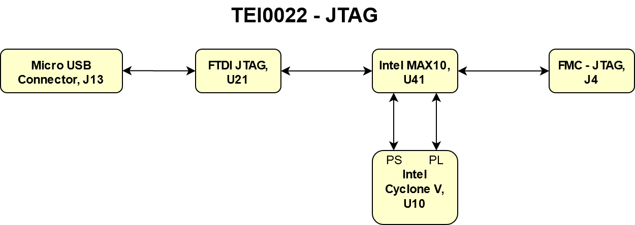
JTAGSEL1
...
JTAGSEL1
...
...
...
...
...
...
...
...
|
Micro USB Connector (UART)
| Anchor | ||||
|---|---|---|---|---|
|
A UART connection between the USB B connector J5 and the Intel Cyclone HPS U10 is possible via the FT234XD (U30) chip.
USB Connector
On the TEI0022 board there are up to four USB 2.0 Hi-Speed ports available (J2, J12).
HDMI Connector
The TEI0022 provides an HDMI Connector J11.
SD Card Connector
SD Card connector J3 is connected to the Intel Cyclone V U10.
RJ45 Connector
The board TEI0022 provides an ethernet interface via the RJ45 connector J1.
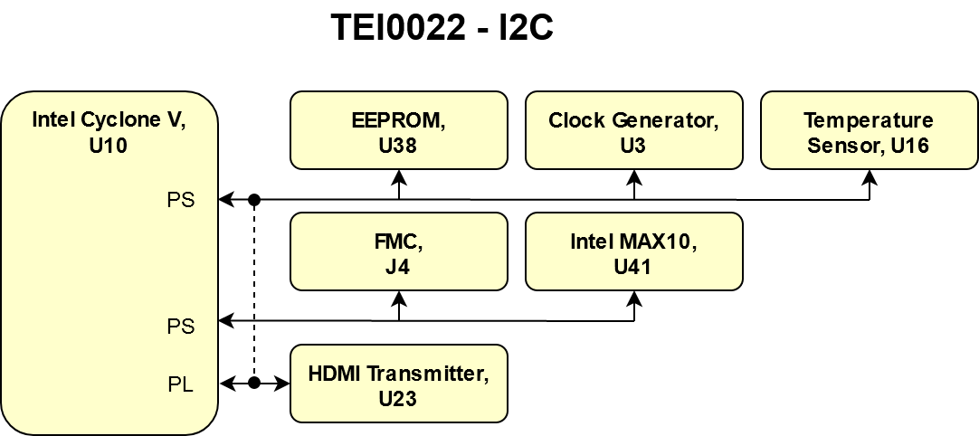
I2C
The TEI0022 provides three independent I2C busses. One bus is used to connect the FMC I2C with the Intel Cyclone V HPS. The second bus is used to connect the HDMI device to the Intel Cyclone V FPGA. The third bus is used to handle the other on-board I2C devices. Via assembly option, it is possible to connect bus two to bus three.
| Scroll Title | ||||||||||||||||||||||||||||
|---|---|---|---|---|---|---|---|---|---|---|---|---|---|---|---|---|---|---|---|---|---|---|---|---|---|---|---|---|
| ||||||||||||||||||||||||||||
|
...
...
...
...
...
...
...
...
...
...
|
On-board Peripherals
...
...
...
...
Notes :
...
...
...
...
...
...
...
...
...
...
...
...
...
...
...
...
...
...
...
...
...
...
...
...
...
...
...
...
...
...
...
...
...
...
...
...
...
...
...
...
...
...
...
...
...
...
...
...
...
...
...
...
...
...
...
...
...
...
...
...
...
...
...
...
...
...
...
...
...
...
...
...
...
...
...
...
...
...
...
| hidden | true |
|---|---|
| id | Comments |
In 'Power and Power-on Sequence' section there are three important digrams which must be drawn:
- Power on-sequence
- Power distribution
- Voltage monitoring circuit
...
...
...
...
|
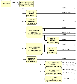
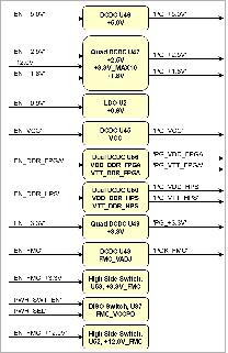
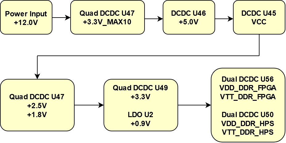
Power-On Sequence
The following figures delivers the power-on sequence information. The figure Power Sequency shows the connections between the power devices and its management. The figure Suggested Power Sequency shows the recommended firmware power-on sequence. For more information about firmware depended power-on sequencing see TEI0022 Intel MAX 10 → Power mangement.
| Scroll Title | |||||
|---|---|---|---|---|---|
| |||||
|
...
...
...
|
| Scroll Title | |||||||||||||||||
|---|---|---|---|---|---|---|---|---|---|---|---|---|---|---|---|---|---|
| |||||||||||||||||
|
...
...
|
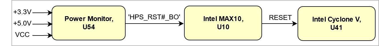
Voltage Monitor Circuit
The voltages +3.3V, +5.0V, and VCC are monitored by the voltage monitor circuit LTC2911 (U54), which generates a reset signal at power-on. A manual reset is also possible as described in the reset table.
| Scroll Title | ||||||||||||||||||||||||||||||||
|---|---|---|---|---|---|---|---|---|---|---|---|---|---|---|---|---|---|---|---|---|---|---|---|---|---|---|---|---|---|---|---|---|
| ||||||||||||||||||||||||||||||||
|
Bank Voltages
| Scroll Title | |||||||||||||||||||||||||||||
|---|---|---|---|---|---|---|---|---|---|---|---|---|---|---|---|---|---|---|---|---|---|---|---|---|---|---|---|---|---|
| |||||||||||||||||||||||||||||
|
...
...
...
...
...
...
|
Currently Offered Variants
| Scroll Ignore | ||
|---|---|---|
|
...
Currently Offered Variants
...
...
...
...
...
...
...
|

Document Change History
| Page properties | ||||
|---|---|---|---|---|
| ||||
|
| Scroll Title | ||||||
|---|---|---|---|---|---|---|
| ||||||
|
...
...
...
--
...
all
...
| Page info | ||||||
|---|---|---|---|---|---|---|
|
...
- Initial Document
Disclaimer
...
| Page info | ||||||
|---|---|---|---|---|---|---|
|
...
change list
Overview
Content Tools