...
The Trenz Electronic TE0703 Carrier Board is a base-board for 4x5 4 x 5 SoMs, which exposes the MIO- and the PS/PL-pins of the SoM to accessible connectors and provides a whole range of on-board-components to test and evaluate Trenz Electronic 4x5 4 x 5 SoMs.
See page "4 x 5 cm carriers" to get information about the SoM's supported by the TE0703 Carrier Board.
...
- On Board:
- USB JTAG and UART interface (FTDI FT2232H), compatible with Xilinx tools (also with many other tools)
- SDIO port expander with voltage-level translation
- 4 x User LEDs
- D1 and D2 are connected to the carrier controller, their function depends on the firmware
- D3 and D4 are connected to the 4 x 5 module B2B connector pins, and are directly controlled by the module
- 1 x User push button
- Connected to "intelligent Carrier Controller (iCC)" and can be used as module reset button. Other usage possible, actual function depend on the code loaded into iCC.
- 4A high efficiency power SoC 6 A DC-DC step-down converter with integrated inductor (Enpirion EN6347) inductor for 3.3V power supply
- 4 User DIP switches
- Enable/disable update of the "intelligent Carrier Controller"
- MIO0 (readable signal by iCC and module)
- 2 "mode" bits
- Interface:
- Trenz 4 x 5 module socket (3 x Samtec LSHM series connectors)
- Micro SD card connector - Zynq SDIO0 bootable SD port
- 2 x VG96 backplane connectors (mounting holes and solder pads)
- Mini USB connector (USB JTAG and UART interface)
- RJ45 GbE connector
- USB host connector
- Power:
- Barrel jack for 5V power supply input
- Dimension:
...
| Scroll Title |
|---|
| anchor | Figure_OV_BD |
|---|
| title | TExxxx TE0703 block diagram |
|---|
|
| Scroll Ignore |
|---|
| draw.io Diagram |
|---|
| border | truefalse |
|---|
| viewerToolbar | true |
|---|
| |
|---|
| fitWindow | false |
|---|
| diagramDisplayName | |
|---|
| lbox | true |
|---|
| revision | 4 |
|---|
| diagramName | BD_TE0703-06 |
|---|
| simpleViewer | false |
|---|
| width | |
|---|
| links | auto |
|---|
| diagramWidthtbstyle | 649top |
|---|
| revisiondiagramWidth | 2640 |
|---|
|
|
| Scroll Only |
|---|
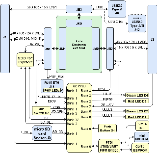 Image Removed Image Removed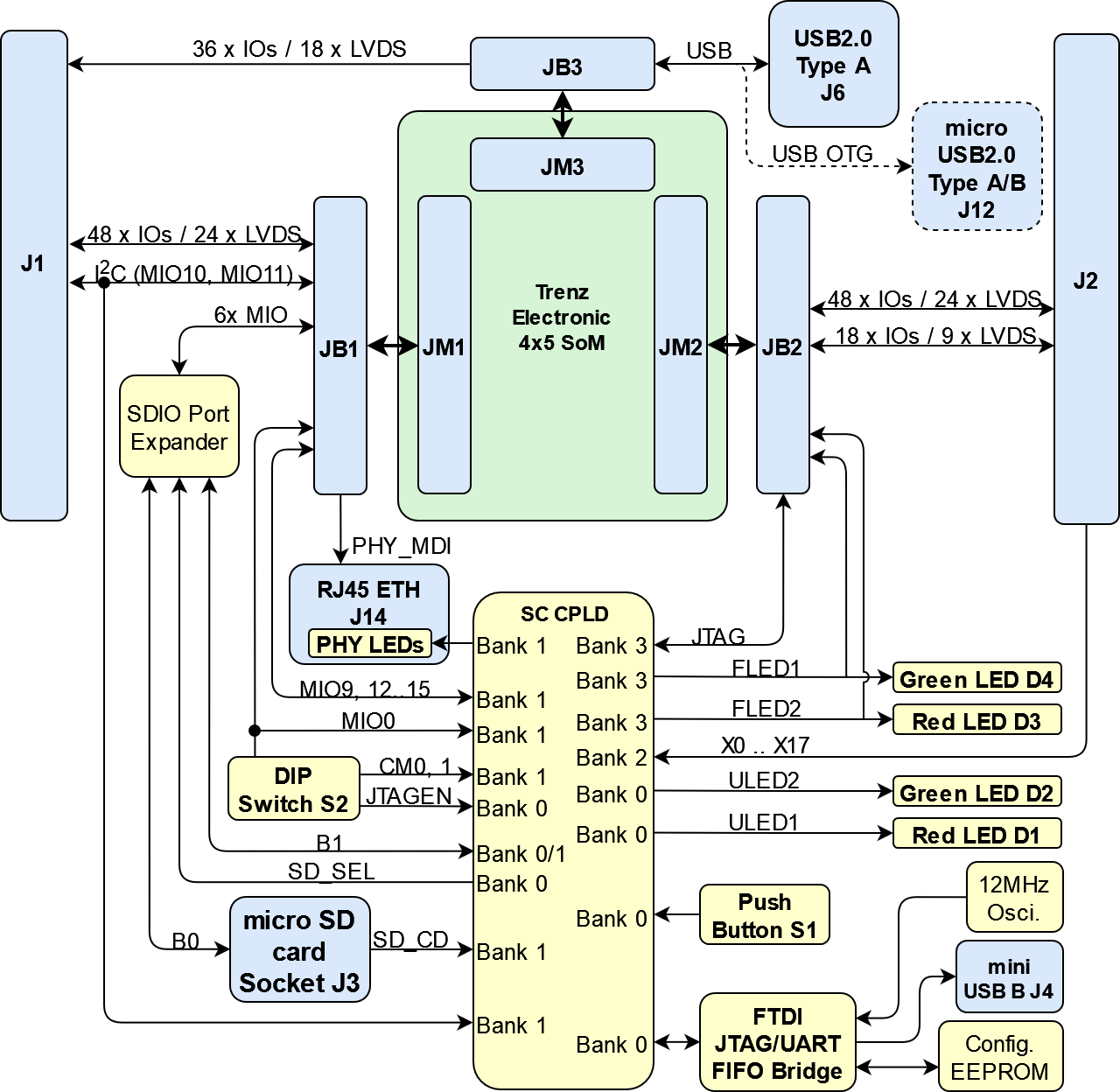 Image Added Image Added
|
|
Main Components
...
| Scroll Title |
|---|
| anchor | Figure_OV_MC |
|---|
| title | TExxxx main components |
|---|
|
| Scroll Ignore |
|---|
| draw.io Diagram |
|---|
| border | truefalse |
|---|
| viewerToolbar | true |
|---|
| |
|---|
| fitWindow | false |
|---|
| diagramDisplayName | |
|---|
| lbox | true |
|---|
| revision | 3 |
|---|
| diagramName | MC_TE0703-06 |
|---|
| simpleViewer | false |
|---|
| width | |
|---|
| links | auto |
|---|
| diagramWidthtbstyle | 641top |
|---|
| revisiondiagramWidth | 2631 |
|---|
|
|
| Scroll Only |
|---|
|
|
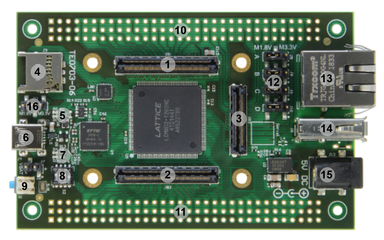
- Samtec Razor Beam™ LSHM-150 B2B connector, JB1
- Samtec Razor Beam™ LSHM-150 B2B connector, JB2
- Samtec Razor Beam™ LSHM-130 B2B connector, JB3
- Micro SD card socket with detect switch, J3
- LED indicators D1 and D2
- Mini-USB type B connector, J4
- LED indicators D3 and D4
- Configuration DIP switches, S2 (see table under "DIP switches" section)
- User push button (Reset), S1
- External connector (VG96) placeholder, J1
- External connector (VG96) placeholder, J2
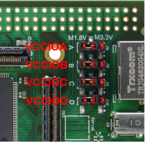
- VCCIO voltage selection jumper block, J5, J8, J9 and J10 (see "Power and Power-On Sequence" section)
- Trxcom 1000Base-T Gigabit RJ45 Magjack, J14 with 4 integrated LEDs
- USB type A receptacle, J6 (optional micro USB 2.0 type A/B receptacle available, J12)
- 5V power connector jack, J13
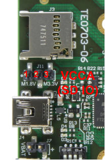
- SD IO voltage (VCCA) selection jumper J11
...
| Scroll Title |
|---|
| anchor | Table_OV_IDS_DIPS |
|---|
| title | Initial delivery state DIP switches |
|---|
|
| Scroll Table Layout |
|---|
| orientation | portrait |
|---|
| sortDirection | ASC |
|---|
| repeatTableHeaders | default |
|---|
| style | |
|---|
| widths | |
|---|
| sortByColumn | 1 |
|---|
| sortEnabled | false |
|---|
| cellHighlighting | true |
|---|
|
| Switch | Position | Description |
|---|
| S2-1 | ON | Mode control MC1. | | S2-2 | ON | FPGA access on module (need also S2-3 ON) | S2-3 | ON | FPGA access on module (need also S2-2 ON) | | S2-4 | OFF | Boot mode set to QSPI. |
|
Different delivery configurations are available upon request.
...
| Scroll Title |
|---|
| anchor | Table_OV_BP |
|---|
| title | Boot process. |
|---|
|
| Scroll Table Layout |
|---|
| orientation | portrait |
|---|
| sortDirection | ASC |
|---|
| repeatTableHeaders | default |
|---|
| style | |
|---|
| widths | |
|---|
| sortByColumn | 1 |
|---|
| sortEnabled | false |
|---|
| cellHighlighting | true |
|---|
|
| Control signal | Switch /Button/ LED /Pin | Signal Schematic Names | Connecte to | Functionality | Notes |
|---|
| Module JTAG select | Dip switche S2-2 | CM0 | SC CPLD pin 75 | ON: Module JTAG access ( if S2-3 ON) OFF: Module CPLD JTAG access ( if S2-3 ON) | TE0703 CPLD - CC703S#CC703S-JTAG | | Module JTAG select | SC CPLD pin 104 | PROGMODE | B2B JB1 pin 90 | Enable B2B Module JTAG access to CPLD for Firmware updateselect: Module CPLD high or SoC/FPGA JTAG low ; via CPLD firmware linked to CM0 | TE0703 CPLD - CC703S#CC703S-JTAG | | Carrier CPLD JTAG enable | Dip switch S2-3 | JTAGEN | SC CPLD pin 120 | ON: SoM JTAG access OFF: Carrier SC CPLD JTAG access | TE0703 CPLD - CC703S#CC703S-JTAG | | Select boot mode | Dip switche S2-4 | MIO0 | SC CPLD pin 94 and B2B JB1 pin 88 | ON: Boot from SD Card OFF: Boot from QSPI flash on module | TE0703 CPLD - CC703S#CC703S-BootMode
Boot Mode is also module dependent | | Select boot mode | SC CPLD pin 83 | MODE | B2B JB1 pin 31 | SD-CARD (Zynq) or QSPI-Flash; via CPLD firmware linked to MIO0 | TE0703 CPLD - CC703S#CC703S-BootMode
Boot Mode is also module dependent | | Reset | S1 | S1 | SC CPLD pin114 | global reset | TE0703 CPLD - CC703S#CC703S-Reset | | Reset | SC CPLD pin 119 | RESIN | B2B JB2 pin 17 | via CPLD firmware linked to S1 | TE0703 CPLD - CC703S#CC703S-Reset | | Moduel enable | SC CPLD pin 81 | EN1 | B2B JB1 pin 27 | Module power enable | pulled up by CPLD | | Disable CPLD power Management | SC CPLD pin 78 | NOSEQ | B2B JB1 pin 8 | Disable CPLD power management | pulled up by CPLD | | Disable Card detect pin | Dip switche S2-1 | CM1 | SC CPLD pin 76 | ON: Force CD Pin to module to GND OFF: Set CD Pin to module to SD CD Pin | TE0703 CPLD - CC703S#CC703S-SD | | SD Card detect | SD Card Socket J3 pin 9 | SD_CD | SC CPLD pin93 | Low if Card detected | TE0703 CPLD - CC703S#CC703S-SD | | SD Selector | SC CPLD pin 113 | SD_SEL | U2 pin 24 | FIXed to GND: Select SD Card (CPLD SD port not used) | TE0703 CPLD - CC703S not used |
|
...
Micro SD card socket is connected to the B2B connector through a Texas Instruments TXS02612 SDIO port expander for voltage translation. The Micro SD card has 3.3V signal voltage level while most 4x5 4 x 5 modules use 1.8V for the SD card interface.
...
| Scroll Title |
|---|
| anchor | Table_SIP_JTG |
|---|
| title | JTAG pins connection |
|---|
|
| Scroll Table Layout |
|---|
| orientation | portrait |
|---|
| sortDirection | ASC |
|---|
| repeatTableHeaders | default |
|---|
| style | |
|---|
| widths | |
|---|
| sortByColumn | 1 |
|---|
| sortEnabled | false |
|---|
| cellHighlighting | true |
|---|
|
Signal | B2B Connector Pin | Note |
|---|
| M_TCK | U5-131 | CPLD Firmware dependent TE0703 CPLD - CC703S#CC703S, dependent on Dip switches linked to Module JTAG Port on JB2. | | M_TDI | U5-136 | | M_TDO | U5-137 | | M_TMS | U5-130 | | FT_B_TX | U5-139 | CPLD Firmware dependent TE0703 CPLD - CC703S#CC703S, linked to Module primary UART on JB1. | | FT_B_RX | U5-138 | | ADBUS7 | U5-142 | CPLD Firmware dependent TE0703 CPLD - CC703S#CC703S, currently not used. | | ADBUS4 | U5-143 | | ACBUS4 | U5-141 | | ACBUS5 | U5-140 | | BDBUS2 | U5-133 | | BDBUS3 | U5-132 | | BDBUS4 | U5-128 | | BDBUS5 | U5-127 | | BDBUS6 | U5-126 | | BDBUS7 | U5-125 | | BCBUS0 | U5-122 | | BCBUS1 | U5-121 |
|
LEDs
There are four on-board LEDs. D3 and D4 are connected to the B2B connector JB2 pins FLED1 and FLED2 respectively and can be read by CPLD firmware.
CPLD
TE0703-06 has a Lattice LCMXO2-1200HC as a system controller. for further function description see Firmware TE0703 CPLD - CC703S#CC703S,
SD IO Levelshifter
SD IO levelshifter (U2) is used in congntion with jumper J11 to select the correct SD IO interface voltage of the SoM.
I2C Repeater
For power sequence reasons the I2C bus is routed via a repater (U7) to to ensure no IOs of the SoM are driven before M3.3VOUT is up.
LEDs
There are four on-board LEDs. D3 and D4 are connected to the B2B connector JB2 pins FLED1 and FLED2 respectively and can be read by CPLD firmware. See TE0703 CPLD - CC703S#CC703S-LED.
| Scroll Title |
|---|
|
| Scroll Title |
|---|
| anchor | Table_OBP_LED |
|---|
| title | On-board LEDs |
|---|
|
| Scroll Table Layout |
|---|
| orientation | portrait |
|---|
| sortDirection | ASC |
|---|
| repeatTableHeaders | default |
|---|
| style | |
|---|
| widths | |
|---|
| sortByColumn | 1 |
|---|
| sortEnabled | false |
|---|
| cellHighlighting | true |
|---|
|
| LED | Color | Signal | Connected to | Description |
|---|
| D1 | Red | ULED1 | U5-117 | FTDI UART receive activity. | | D2 | Green | ULED2 | U5-115 | FTDI UART transmit activity. | | D3 | Red | FLED1 | JB2-99 | Module LED, CPLD can read status via signal FL_0 connected via 10K. | | D4 | Green | FLED2 | JB2-90 | Module LED, CPLD can read status via signal FL_1 connected via 10K. |
|
DIP switches
DIP switch settings are CPLD Firmware dependent, default firmware:
| Scroll Title |
|---|
| anchor | Table_OBP_DIS |
|---|
| title | Dip-Switches |
|---|
|
| Scroll Table Layout |
|---|
| orientation | portrait |
|---|
| sortDirection | ASC |
|---|
| repeatTableHeaders | default |
|---|
| style | |
|---|
| widths | |
|---|
| sortByColumn | 1 |
|---|
| sortEnabled | false |
|---|
| cellHighlighting | true |
|---|
|
| Switch | ON | OFF | Notes |
|---|
| S2-1 | Set PGOOD pin to low ('0') / Force CD |
Pin GNDset CD Pin | high impedance ('Z') | Set PGOOD pin to high ('1') / Set CD pin to module to SD_CD |
Pin 3| 2) | Carrier CPLD JTAG access |
Boot set Pin | Set pin to GND) | Boot from QSPI flash on module ( |
set Pin is also module depends
|
Mode status is displayed on TE0703 LEDs, see TE0703 CPLD - CC703S#CC703S-LED.
Jumper
TE0703-06 has 5 Voltage selection jumpers. Select 1.8V or 3.3V in accordenc of the attached module capabilities and your needs. Refer to the 4x5 4 x 5 Module Integration Guide for VCCIO voltages options.
| Scroll Title |
|---|
| anchor | Table_OBP_JUM |
|---|
| title | Jumpers |
|---|
|
| Scroll Table Layout |
|---|
| orientation | portrait |
|---|
| sortDirection | ASC |
|---|
| repeatTableHeaders | default |
|---|
| style | |
|---|
| widths | |
|---|
| sortByColumn | 1 |
|---|
| sortEnabled | false |
|---|
| cellHighlighting | true |
|---|
|
| Power Rail | Jumper | 1.8V | 3.3V | Notes |
|---|
| VCCIOA | J5 | 1-2 | 2-3 | - | | VCCIOB | J8 | 1-2 | 2-3 | - | | VCCIOC | J9 | 1-2 | 2-3 | - | | VCCIOD | J10 | 1-2 | 2-3 | - | | VCCA | J11 | 1-2 | 2-3 | SD IO level shifter |
Voltage Selection| voltage selection (module side), compare with TRM of attached Module |
|
| Scroll Title |
|---|
| anchor | Figure_OVOBP_MCJUM |
|---|
| title | TExxxx main componentsTE0703 Jumper Settings |
|---|
|
| Scroll Ignore |
|---|
| draw.io Diagram |
|---|
| border | truefalse |
|---|
| viewerToolbar | true |
|---|
| |
|---|
| fitWindow | false |
|---|
| diagramDisplayName | |
|---|
| lbox | true |
|---|
| revision | 4 |
|---|
| diagramName | JUM_TE0703-06_SD |
|---|
| simpleViewer | false |
|---|
| width | |
|---|
| links | auto |
|---|
| tbstylediagramWidth | 277top |
|---|
| revisiondiagramWidth | 2275 |
|---|
|
| draw.io Diagram |
|---|
| border | truefalse |
|---|
| viewerToolbar | true |
|---|
| |
|---|
| fitWindow | false |
|---|
| diagramDisplayName | |
|---|
| lbox | true |
|---|
| revision | 3 |
|---|
| diagramName | JUM_TE0703-06 |
|---|
| simpleViewer | false |
|---|
| width |
|---|
| diagramWidth | 431 |
|---|
| | links | auto |
|---|
| tbstyle | top |
|---|
| diagramWidth | 432 | revision | 2 |
|---|
|
|
| Scroll Only |
|---|
|
|
| Note |
|---|
Take care of the VCCO voltage ranges of the particular PL IO-banks (HR, HP) of the mounted SoM, otherwise damages may occur to the FPGA. Therefore, refer to the TRM of the mounted SoM to get the specific information of the voltage ranges. It is recommended to set and measure the PL IO-bank supply-voltages before mounting of TE 4 x 5 module to avoid failures and damages to the functionality of the mounted SoM. |
...
| Scroll Title |
|---|
| anchor | Table_PWR_PC |
|---|
| title | Power Consumption |
|---|
|
| Scroll Table Layout |
|---|
| orientation | portrait |
|---|
| sortDirection | ASC |
|---|
| repeatTableHeaders | default |
|---|
| style | |
|---|
| widths | |
|---|
| sortByColumn | 1 |
|---|
| sortEnabled | false |
|---|
| cellHighlighting | true |
|---|
|
| Power Input Pin | Max Current |
|---|
| VIN (power connector jack J13) | 4A |
|
Typical power consumption for TE0703-05 + TE0715-01 module with SD micro card inserted, Ethernet connected and link up, system booted into Linux prompt and idling is 5V / 0.55A.
...
| Scroll Title |
|---|
| anchor | Table_PWR_PR |
|---|
| title | Module power rails. |
|---|
|
| Scroll Table Layout |
|---|
| orientation | portrait |
|---|
| sortDirection | ASC |
|---|
| repeatTableHeaders | default |
|---|
| style | |
|---|
| widths | |
|---|
| sortByColumn | 1 |
|---|
| sortEnabled | false |
|---|
| cellHighlighting | true |
|---|
|
| Power Rail Name | Connector-Pin | Direction | Notes |
|---|
| 5VIN | J13-1 | in | 5 V power input | | VIN | - | - | 5 V power input after protection | | 3.3V | JB1-2, 4, 6, 14, 16 | out | Generatet from VIN by DCDC U3, constant 3.3V rail | | M1.8VOUT | JB1-40 | in | 1.8V from Module. | | M3.3VOUT | JB2-9, 11 | in | 3.3V from Module. | | VCCIOA | JB1-10, 12 | out | Use jumper J5 to source by M1.8VOUT or M3.3VOUT. | | VCCIOB | JB2-2 ,4 | out | Use jumper J8 to source by M1.8VOUT or M3.3VOUT. | | VCCIOC | JB2-6 | out | Use jumper J9 to source by M1.8VOUT or M3.3VOUT. | VCCIOD | JB2-8, 10 | out | | JB2-8, 10 | out | Use jumper J10 to source by M1.8VOUT or M3.3VOUT. | | VCCA | - | - | SD IO leveshifter voltge on Module side. Use jumper J11 Use jumper J10 to source by M1.8VOUT or M3.3VOUT. | | VCCJTAG | JB2-92 | in | JTAG reference voltage | | USB-VBUS_R | J6-1 (J12-1) | out | 5V USB, derived from VIN by power switch U1 |
|
...
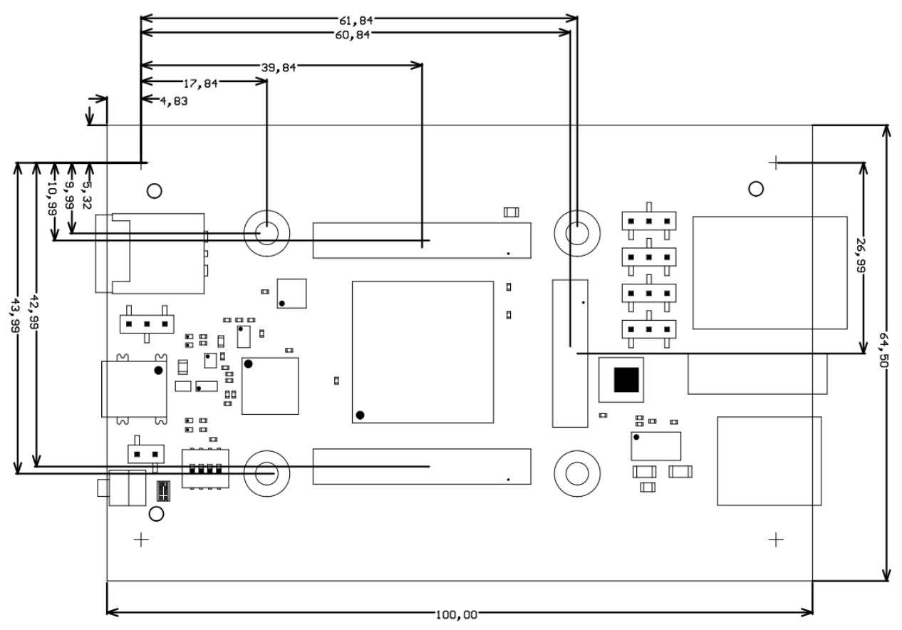
| Scroll Title |
|---|
| anchor | Figure_TS_PD |
|---|
| title | Physical Dimension |
|---|
|
| Scroll Ignore |
|---|
| draw.io Diagram |
|---|
| border | truefalse |
|---|
| viewerToolbar | true |
|---|
| |
|---|
| fitWindow | false |
|---|
| diagramDisplayName | |
|---|
| lbox | true |
|---|
| revision | 4 |
|---|
| diagramName | PD_TE0703-06_top |
|---|
| simpleViewer | false |
|---|
| width | |
|---|
| links | auto |
|---|
| tbstyle | top |
|---|
| diagramWidth | 633 | revision | 2 |
|---|
|
| draw.io Diagram |
|---|
| border | truefalse |
|---|
| viewerToolbar | true |
|---|
| |
|---|
| fitWindow | false |
|---|
| diagramDisplayName | |
|---|
| lbox | true |
|---|
| revision | 4 |
|---|
| diagramName | PD_TE0703-06_bottom |
|---|
| simpleViewer | false |
|---|
| width | 600 |
|---|
| links | auto |
|---|
| tbstyle | top |
|---|
| diagramWidth | 633 | revision | 2 |
|---|
|
|
| Scroll Only |
|---|
| scroll-pdf | true |
|---|
| scroll-office | true |
|---|
| scroll-chm | true |
|---|
| scroll-docbook | true |
|---|
| scroll-eclipsehelp | true |
|---|
| scroll-epub | true |
|---|
| scroll-html | true |
|---|
|
  |
|
...
Hardware Revision History
Date | Revision | Notes | PCN | Documents |
|---|
| 2023-09-04 | 07 | See Revision changes. |
|
|
| 2019-09-02 | 06 | Added SD IO | voltage selection jumpervoltage selection jumper Further changes see PCN. | PCN- | 2016112220190104 | TE0703 |
2016-09-07 | 05 | Added VCCIO Jumpers | PCN-20161122 | TE0703-05 |
- | 04 | Corrected FTDI EEPROM connection | - | TE0703-04 |
- | 03 | Added VCCIO strapping resistors | - |
|
- | 02 | First series boards | - |
|
- | 01 | Prototypes | - |
|
Hardware revision number is printed on the PCB board next to the module model number separated by the dash.
| draw.io Diagram |
|---|
| border | truefalse |
|---|
| viewerToolbar | true |
|---|
| |
|---|
| fitWindow | false |
|---|
| diagramDisplayName | |
|---|
| lbox | true |
|---|
| revision | 3 |
|---|
| diagramName | REV_TE0703-06 |
|---|
| simpleViewer | false |
|---|
| width | 200 |
|---|
| links | 400auto |
|---|
| diagramWidthtbstyle | 199top |
|---|
| revisiondiagramWidth | 1194 |
|---|
|
Document Change History
Date | Revision | Contributors | Description |
|---|
| Page info |
|---|
| infoType | Modified date |
|---|
| dateFormat | yyyy-MM-dd |
|---|
| type | Flat |
|---|
|
| | Page info |
|---|
| infoType | Current version |
|---|
| prefix | v. |
|---|
| type | Flat |
|---|
| showVersions | false |
|---|
|
| | Page info |
|---|
| infoType | Modified by |
|---|
| type | Flat |
|---|
| showVersions | false |
|---|
|
| |
| 2022-09-23 | v.44 | Mohsen Chamanbaz | - Changing in the dip-switches table because of updating of CPLD firmware (CPLD Firmware REV03)
|
| 2019-10-07 | v.43 | Martin Rohrmüller | | updating - updated to TRM style 2.12
|
| | Ali Naseri | - updating operating conditions
|
| 2017-02-07 | v.28 | John Hartfiel | - Add DIP setting description
|
| 2017-11-09 | v.26 | John Hartfiel | - add B2B connector section
|
| 2017-02-21 | | Jan Kumann | |
| 2017-02-02 | | Jan Kumann | - New board image with silk screen pin markings for VG96 connectors J1 and J2.
|
| 2016-12-22 | | Jan Kumann | |
| 2016-12-08 | v.10 | | - Document structure revised.
|
| 2016-12-05 | | John Hartfiel | - Corrected Boot Mode table.
|
| 2016-09-06 | | Jan Kumann, John Hartfiel | |
Disclaimer
| Include Page |
|---|
| IN:Legal Notices |
|---|
| IN:Legal Notices |
|---|
|
...