Page History
...
| Scroll pdf ignore | |
|---|---|
Table of Contents
|
Overview
The Trenz Electronic TEM0005-02 is a low-cost
...
module with Microsemi SmartFusion2
...
SoC and 32 MByte flash memory for configuration and operation. SmartFusion2 combines a 166 MHz Cortex-M3 MCU with 256 KByte Flash and 80 KByte SRAM as well as 12 kLUT FPGA Core Logic.
Refer to http://trenz.org/tem0005-info for the current online version of this manual and other available documentation.
...
- SoC/FPGA
- Package: VFG400
- Device: M2S005, M2S010, M2S025, M2S050 ,M2S060 *
- Engine: VFG166Mhz 32Bit ARM Cortex-M3
- Speed: -1, Standard*, **
- Temperature: C, I,*, **
- RAM/Storage
- Low Power DDR3
- Data width: 8/ 16bit
- Size: def. 2Gb*
- Speed: 20ns***
- SPI Flash
- size: 256 M bit * bit
- 2Kb EEPROM
- Low Power DDR3
- On Board
- Crypto Authentication IC
- Voltage monitor IC
- 10/100 Mbps PHY Ethernet
- Interface
- Samtec ST5 B2B Connector
- Power
- 5V 3.3V supplied from carrier
- Dimension
- 56 x 31 mm
- Notes
- * depends on assembly version
- ** also non low power assembly options possible
- *** depends on used FPGA and DDR3 combination
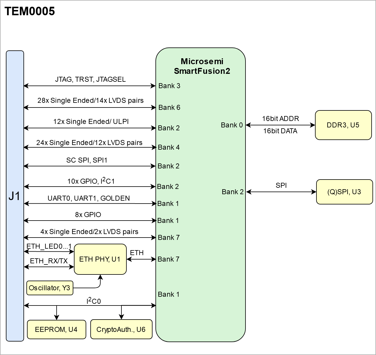
Block Diagram
| Page properties | ||||
|---|---|---|---|---|
| ||||
add drawIO object here.
|
...
| Scroll Title | |||||||||||||||||||||||||||||||||||||||||||||||||
|---|---|---|---|---|---|---|---|---|---|---|---|---|---|---|---|---|---|---|---|---|---|---|---|---|---|---|---|---|---|---|---|---|---|---|---|---|---|---|---|---|---|---|---|---|---|---|---|---|---|
| |||||||||||||||||||||||||||||||||||||||||||||||||
|
Main Components
...
| Scroll Title | ||||||||||||||||||||||||||||
|---|---|---|---|---|---|---|---|---|---|---|---|---|---|---|---|---|---|---|---|---|---|---|---|---|---|---|---|---|
| ||||||||||||||||||||||||||||
|
- ...
- ...
- ...
Initial Delivery State
- Microsemi SmartFusion2 SoC, U2
- Dual DCDC Regulator, U7
- EEPROM, U4
- 10/100 Mb Ethernet, U1
- QSPI Flash, U3
- Authentication IC, U6
- DDR3 Memory, U5
- B2B Connector, J1
Initial Delivery State
| Page properties | ||||
|---|---|---|---|---|
| ||||
| Page properties | ||||
| ||||
Notes : Only components like EEPROM, QSPI flash can be initialized by default at manufacture. If there is no components which might have initial data ( possible on carrier) you must keep the table empty |
...
| Scroll Title | ||||||||||||||||||||||||||||||
|---|---|---|---|---|---|---|---|---|---|---|---|---|---|---|---|---|---|---|---|---|---|---|---|---|---|---|---|---|---|---|
| ||||||||||||||||||||||||||||||
|
Configuration Signals
| Page properties | ||||
|---|---|---|---|---|
| ||||
|
...
| Scroll Title | |||||||||||||||||||||
|---|---|---|---|---|---|---|---|---|---|---|---|---|---|---|---|---|---|---|---|---|---|
| |||||||||||||||||||||
MODE
Boot Mode | | ||||||||||||||||||||
| Scroll Title | |||||||||||||||||||||
| |||||||||||||||||||||
| Scroll Table Layout | |||||||||||||||||||||
| orientation | portrait | ||||||||||||||||||||
| sortDirection | ASC | ||||||||||||||||||||
| repeatTableHeaders | default | style | widths | ||||||||||||||||||
| sortByColumn | 1 | ||||||||||||||||||||
| sortEnabled | false | ||||||||||||||||||||
| cellHighlighting | true | ||||||||||||||||||||
Signal | B2B | I/O | Note |
Signals, Interfaces and Pins
|
Signals, Interfaces and Pins
| Page properties | ||||
|---|---|---|---|---|
| ||||
Notes :
| ||||
| Page properties | ||||
| ||||
Notes :
|
...
FPGA bank number and number of I/O signals connected to the B2B connector:, J1.
| Scroll Title | |||||||||||||||||||||||
|---|---|---|---|---|---|---|---|---|---|---|---|---|---|---|---|---|---|---|---|---|---|---|---|
| |||||||||||||||||||||||
|
...
JTAG access to the TExxxx SoM through B2B connector JMX.
...
| anchor | Table_SIP_JTG |
|---|---|
| title | JTAG pins connection |
...
JTAG Signal
...
B2B Connector
...
MIO Pins
...
| hidden | true |
|---|---|
| id | Comments |
you must fill the table below with group of MIOs which are connected to a specific components or peripherals, you do not have to specify pins in B2B, Just mention which B2B is connected to MIOs. The rest is clear in the Schematic.
Example:
...
SPI_CS , SPI_DQ0... SPI_DQ3
SPI_SCK
...
| anchor | Table_SIP_MIOs |
|---|---|
| title | MIOs pins |
...
Test Points
...
| hidden | true |
|---|---|
| id | Comments |
you must fill the table below with group of Test Point which are indicated as TP in a schematic. If there is no Test Point remarked in the schematic, delet the Test Point section.
Example:
...
| anchor | Table_SIP_TPs |
|---|---|
| title | Test Points Information |
...
On-board Peripherals
| Page properties | ||||
|---|---|---|---|---|
| ||||
Notes :
|
| Page properties | ||||
|---|---|---|---|---|
| ||||
Notes : In the on-board peripheral table "chip/Interface" must be linked to the corresponding chapter or subsection |
...
| anchor | Table_OBP |
|---|---|
| title | On board peripherals |
...
Quad SPI Flash Memory
| Page properties | ||||
|---|---|---|---|---|
| ||||
Notes : Minimum and Maximum density of quad SPI flash must be mentioned for other assembly options. |
...
| anchor | Table_OBP_SPI |
|---|---|
| title | Quad SPI interface MIOs and pins |
...
| anchor | Table_OBP_RTC |
|---|---|
| title | I2C interface MIOs and pins |
...
| anchor | Table_OBP_I2C_RTC |
|---|---|
| title | I2C Address for RTC |
...
| anchor | Table_OBP_EEP |
|---|---|
| title | I2C EEPROM interface MIOs and pins |
...
| anchor | Table_OBP_I2C_EEPROM |
|---|---|
| title | I2C address for EEPROM |
...
LEDs
...
| anchor | Table_OBP_LED |
|---|---|
| title | On-board LEDs |
...
DDR3 SDRAM
| Page properties | ||||
|---|---|---|---|---|
| ||||
Notes : Minimum and Maximum density of DDR3 SDRAM must be mentioned for other assembly options. (pay attention to supported address length for DDR3) |
The TE???? SoM has ??? GByte volatile DDR3 SDRAM IC for storing user application code and data.
- Part number:
- Supply voltage:
- Speed:
- NOR Flash
- Temperature:
Ethernet
...
| anchor | Table_OBP_ETH |
|---|---|
| title | Ethernet PHY to Zynq SoC connections |
...
CAN Transceiver
...
| anchor | Table_OBP_CAN |
|---|---|
| title | CAN Tranciever interface MIOs |
...
| anchor | Table_OBP_CLK |
|---|---|
| title | Osillators |
...
Programmable Clock Generator
There is a programmable clock generator on-board (U??) provided in order to generate variable clocks for the module. Programming can be done using I2C via PIN header J??. The I2C Address is 0x??.
...
| anchor | Table_OBP_PCLK |
|---|---|
| title | Programmable Clock Generator Inputs and Outputs |
| Scroll Table Layout | ||||||||||||
|---|---|---|---|---|---|---|---|---|---|---|---|---|
|
...
IN0
...
XAXB
...
Power and Power-On Sequence
...
| hidden | true |
|---|---|
| id | Comments |
In 'Power and Power-on Sequence' section there are three important digrams which must be drawn:
- Power on-sequence
- Power distribution
- Voltage monitoring circuit
| Note |
|---|
For more information regarding how to draw diagram, Please refer to "Diagram Drawing Guidline" . |
Power Supply
Power supply with minimum current capability of xx A for system startup is recommended.
Power Consumption
...
| anchor | Table_PWR_PC |
|---|---|
| title | Power Consumption |
...
* TBD - To Be Determined
Power Distribution Dependencies
...
| anchor | Figure_PWR_PD |
|---|---|
| title | Power Distribution |
...
| Scroll Only |
|---|
|
Power-On Sequence
...
| anchor | Figure_PWR_PS |
|---|---|
| title | Power Sequency |
...
| Scroll Only |
|---|
|
Voltage Monitor Circuit
...
| anchor | Figure_PWR_VMC |
|---|---|
| title | Voltage Monitor Circuit |
| Scroll Ignore |
|---|
Create DrawIO object here: Attention if you copy from other page, objects are only linked. |
| Scroll Only |
|---|
image link to the generate DrawIO PNG file of this page. This is a workaround until scroll pdf export bug is fixed |
|
JTAG Interface
JTAG access to the TEM0005 SoM through B2B connector J1.
Power Rails
...
| anchor | Table_PWR_PR |
|---|---|
| title | Module power rails. |
...
B2B Connector
JM1 Pin
...
B2B Connector
JM2 Pin
...
B2B Connector
JM3 Pin
...
Bank Voltages
...
| anchor | Table_PWR_BV |
|---|---|
| title | Zynq SoC bank voltages. |
...
Bank
...
Voltage
...
| hidden | true |
|---|---|
| id | Comments |
...
use "include page" macro and link to the general B2B connector page of the module series,
...
Technical Specifications
Absolute Maximum Ratings
...
| anchor | Table_TS_AMR |
|---|---|
| title | PS absolute maximum ratings |
...
Recommended Operating Conditions
Operating temperature range depends also on customer design and cooling solution. Please contact us for options.
...
| anchor | Table_TS_ROC |
|---|---|
| title | Recommended operating conditions. |
...
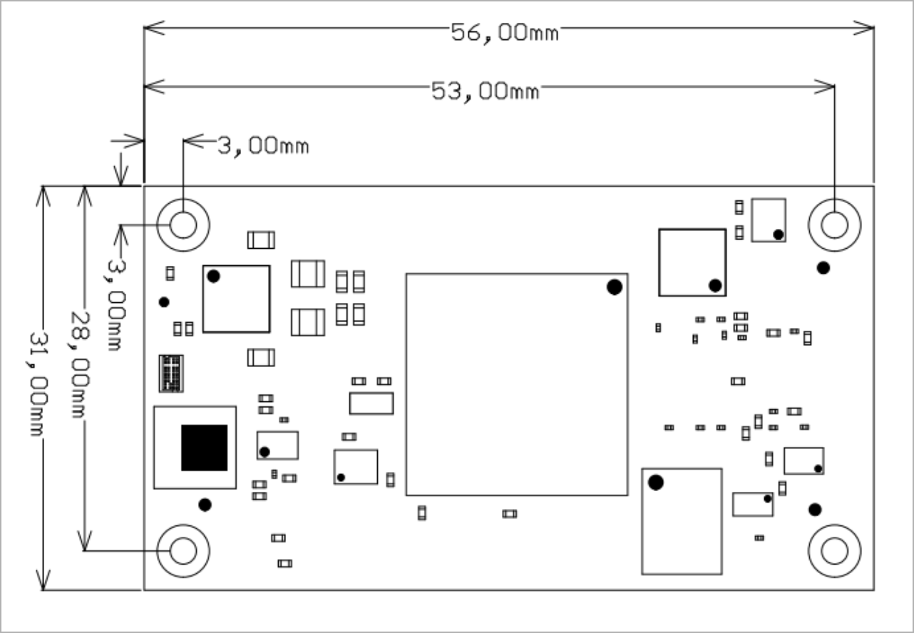
Physical Dimensions
Module size: ?? mm × ?? mm. Please download the assembly diagram for exact numbers.
Mating height with standard connectors: ? mm.
PCB thickness: ?? mm.
...
| hidden | true |
|---|---|
| id | Comments |
In 'Physical Dimension' section, top and bottom view of module must be inserted, information regarding physical dimensions can be obtained through webpage for product in Shop.Trenz, (Download> Documents> Assembly part) for every SoM.
For Example: for Module TE0728, Physical Dimension information can be captured by snipping tools from the link below:
| Note |
|---|
For more information regarding how to draw diagram, Please refer to "Diagram Drawing Guidline" . |
...
| anchor | Figure_TS_PD |
|---|---|
| title | Physical Dimension |
...
| Scroll Only | ||||||||||||||
|---|---|---|---|---|---|---|---|---|---|---|---|---|---|---|
| ||||||||||||||
|
Currently Offered Variants
| Page properties | ||||
|---|---|---|---|---|
| ||||
Set correct link to the shop page overview table of the product on English and German. Example for TE0706: ENG Page: https://shop.trenz-electronic.de/en/search?sSearch=TE0706 DEU Page: https://shop.trenz-electronic.de/de/search?sSearch=TE0706 |
...
| anchor | Table_VCP_SO |
|---|---|
| title | Trenz Electronic Shop Overview |
...
Revision History
Hardware Revision History
| Page properties | ||||
|---|---|---|---|---|
| ||||
Set correct links to download arrier, e.g. TE0706 REV02: TE0706-02 -> https://shop.trenz-electronic.de/Download/?path=Trenz_Electronic/Modules_and_Module_Carriers/4x5/4x5_Carriers/TE0706/REV02/Documents Note:
|
...
| anchor | Table_RH_HRH |
|---|---|
| title | Hardware Revision History |
...
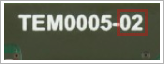
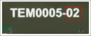
Hardware revision number can be found on the PCB board together with the module model number separated by the dash.
...
| anchor | Figure_RV_HRN |
|---|---|
| title | Board hardware revision number. |
...
| Scroll Only |
|---|
|
Document Change History
| Page properties | ||||
|---|---|---|---|---|
| ||||
|
...
| anchor | Table_RH_DCH |
|---|---|
| title | Document change history. |
...
| Page info | ||||||
|---|---|---|---|---|---|---|
|
...
| Page info | ||||||||
|---|---|---|---|---|---|---|---|---|
|
...
| Page info | ||||||
|---|---|---|---|---|---|---|
|
...
change list
...
--
...
all
...
| Page info | ||||||
|---|---|---|---|---|---|---|
|
...
- --
Disclaimer
...
| Page properties | ||||
|---|---|---|---|---|
| ||||
Template Revision 2.12
|
| HTML |
|---|
<!-- tables have all same width (web max 1200px and pdf full page(640px), flexible width or fix width on menu for single column can be used as before) -->
<style>
.wrapped{
  width: 100% !important;
  max-width: 1200px !important;
 }
</style> |
...
| hidden | true |
|---|---|
| id | Comments |
Important General Note:
...
Designate all graphics and pictures with a number and a description, Use "Scroll Title" macro
...
Figure template:
...
| anchor | Figure_anchorname |
|---|---|
| title | Text |
| Scroll Ignore |
|---|
Create DrawIO object here: Attention if you copy from other page, objects are only linked. |
| Scroll Only |
|---|
image link to the generate DrawIO PNG file of this page. This is a workaround until scroll pdf export bug is fixed |
...
Table template:
- Layout macro can be use for landscape of large tables
...
| anchor | Table_tablename |
|---|---|
| title | Text |
...
The anchors of the Scroll Title should be named consistant across TRMs. A incomplete list of examples is given below
<type>_<main section>_<name>
- type: Figure, Table
- main section:
- "OV" for Overview
- "SIP" for Signal Interfaces and Pins,
- "OBP" for On board Peripherals,
- "PWR" for Power and Power-On Sequence,
- "B2B" for Board to Board Connector,
- "TS" for Technical Specification
- "VCP" for Variants Currently in Production
- "RH" for Revision History
- name: custom, some fix names, see below
- Fix names:
"Figure_OV_BD" for Block Diagram
"Figure_OV_MC" for Main Components
"Table_OV_IDS" for Initial Delivery State
"Table_PWR_PC" for Power Consumption
- "Figure_PWR_PD" for Power Distribution
- "Figure_PWR_PS" for Power Sequence
- "Figure_PWR_PM" for Power Monitoring
- "Table_PWR_PR" for Power Rails
- "Table_PWR_BV" for Bank Voltages
"Table_TS_AMR" for Absolute_Maximum_Ratings
"Table_TS_ROC" for Recommended_Operating_Conditions
- "Figure_TS_PD" for Physical_Dimensions
- "Table_VCP_SO" for TE_Shop_Overview
"Table_RH_HRH" for Hardware_Revision_History
- "Figure_RH_HRN" for Hardware_Revision_Number
- "Table_RH_DCH" for Document_Change_History
...
| Page properties | ||||
|---|---|---|---|---|
| ||||
----------------------------------------------------------------------- |
| Page properties | ||||
|---|---|---|---|---|
| ||||
Note for Download Link of the Scroll ignore macro:
|
| Scroll Ignore |
|---|
| Scroll pdf ignore | |
|---|---|
Table of Contents
|
Overview
The Trenz Electronic TE0xxx-xx ... is an industrial-grade ... module ... based on Xilinx ...
Refer to http://trenz.org/tem0005-info for the current online version of this manual and other available documentation.
| Page properties | ||||
|---|---|---|---|---|
| ||||
Notes :
|
Key Features
...
| hidden | true |
|---|---|
| id | Comments |
Note:
'description: Important components and connector or other Features of the module
→ please sort and indicate assembly options
Key Features' must be split into 6 main groups for modules and mainboards:
- SoC/FPGA
- Package: SFVC784
- Device: ZU2...ZU5*
- Engine: CG, EG, EV*
- Speed: -1LI, -2LE,*, **
- Temperature: I, E,*, **
- RAM/Storage
- Low Power DDR4 on PS
- Data width: 32bit
- Size: def. 2GB*
- Speed:***
- eMMC
- Data width: 8Bit
- size: def. 8GB *
- QSPI boot Flash in dual parallel mode (size depends on assembly version)
- Data width: 8bit
- size: def. 128MB *
- HyperRAM/Flash (optional, default not assembled)
- size:*
- MAC address serial EEPROM with EUI-48™ node identity (Microchip 24AA025E48)
- Low Power DDR4 on PS
- On Board
- Lattice LCMXO2
- PLL SI5338
- Gigabit Ethernet transceiver PHY (Marvell Alaska 88E1512)
- Hi-speed USB2 ULPI transceiver with full OTG support (Microchip USB3320C)
- Interface
- 132 x HP PL I/Os (3 banks)
- ETH
- USB
- 4 GTR (for USB3, Sata, PCIe, DP)
- MIO for UART
- MIO for SD
- MIO for PJTAG
- JTAG
- Ctrl
- Power
- 3.3V-5V Main Input
- 3.3V Controller Input
- Variable Bank IO Power Input
- Dimension
- 4 cm x 5 cm
- Notes
- * depends on assembly version
- ** also non low power assembly options possible
- *** depends on used U+ Zynq and DDR4 combination
Key Features' must be split into 6 main groups for carrier:
- Modules
- TE0808, TE807, TE0803,...
- RAM/Storage
- E.g. SDRAM, SPI
- On Board
- E.g. CPLD, PLL
- Interface
- E.g. ETH, USB, B2B, Display port
- Power
- E.g. Input supply voltage
- Dimension
- <Replace for module use "SoC/FPGA" for Carrier "Modules">
- ...
- RAM/Storage
- ...
- On Board
- ...
- Interface
- ...
- Power
- ...
- Dimension
- ...
- Notes
- ...
Block Diagram
...
| hidden | true |
|---|---|
| id | Comments |
add drawIO object here.
| Note |
|---|
For more information regarding how to draw a diagram, Please refer to "Diagram Drawing Guidline" . |
...
| anchor | Figure_OV_BD |
|---|---|
| title | TEM0005 block diagram |
...
| Scroll Only |
|---|
|
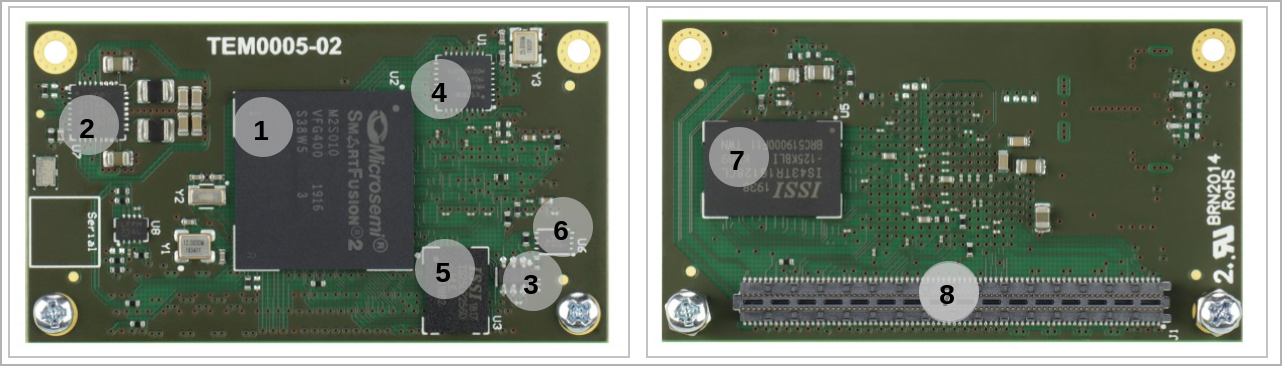
Main Components
...
| hidden | true |
|---|---|
| id | Comments |
Notes :
- Picture of the PCB (top and bottom side) with labels of important components
- Add List below
| Note |
|---|
For more information regarding how to add board photoes, Please refer to "Diagram Drawing Guidline" . |
...
| anchor | Figure_OV_MC |
|---|---|
| title | TEM0005 main components |
...
| Scroll Only |
|---|
|
- ...
- ...
- ...
Initial Delivery State
| Page properties | ||||
|---|---|---|---|---|
| ||||
Notes : Only components like EEPROM, QSPI flash can be initialized by default at manufacture. If there is no components which might have initial data ( possible on carrier) you must keep the table empty |
...
| anchor | Table_OV_IDS |
|---|---|
| title | Initial delivery state of programmable devices on the module |
...
Storage device name
...
Content
...
Notes
...
Quad SPI Flash
...
Configuration Signals
| Page properties | ||||
|---|---|---|---|---|
| ||||
|
...
| anchor | Table_OV_BP |
|---|---|
| title | Boot process. |
...
MODE Signal State
...
| anchor | Table_OV_RST |
|---|---|
| title | Reset process. |
...
Signal
...
Signals, Interfaces and Pins
| Page properties | ||||
|---|---|---|---|---|
| ||||
Notes :
|
Board to Board (B2B) I/Os
FPGA bank number and number of I/O signals connected to the B2B connector:
...
| anchor | Table_SIP_B2B |
|---|---|
| title | General PL I/O to B2B connectors information |
...
JTAG access to the TExxxx SoM through B2B connector JMX.
...
| anchor | Table_SIP_JTG |
|---|---|
| title | JTAG pins connection |
...
JTAG Signal
...
B2B Connector
...
MIO Pins
| Page properties | ||||||||||||||||||||||||||||||||||
|---|---|---|---|---|---|---|---|---|---|---|---|---|---|---|---|---|---|---|---|---|---|---|---|---|---|---|---|---|---|---|---|---|---|---|
| ||||||||||||||||||||||||||||||||||
| MIO Pin | Connected to | B2B | Notes | |||||||||||||||||||||||||||||||
| MIO12...14 | SPI_CS , SPI_DQ0... SPI_DQ3 SPI_SCK | J2 | QSPI | |||||||||||||||||||||||||||||||
| Scroll Title | ||||||||||||||||||||||||||||||||||
| ||||||||||||||||||||||||||||||||||
MIO Pin | Connected to | B2B | Notes |
Test Points
| Page properties | ||||||||
|---|---|---|---|---|---|---|---|---|
| ||||||||
you must fill the table below with group of Test Point which are indicated as TP in a schematic. If there is no Test Point remarked in the schematic, delet the Test Point section. Example:
|
...
| Scroll Title | ||||||||||||||||||||||||||
|---|---|---|---|---|---|---|---|---|---|---|---|---|---|---|---|---|---|---|---|---|---|---|---|---|---|---|
| ||||||||||||||||||||||||||
|
On-board Peripherals
| Page properties | ||||
|---|---|---|---|---|
| ||||
Notes :
|
...
| Scroll Title | |||||||||||||||||||||||||||||||||||||||
|---|---|---|---|---|---|---|---|---|---|---|---|---|---|---|---|---|---|---|---|---|---|---|---|---|---|---|---|---|---|---|---|---|---|---|---|---|---|---|---|
| |||||||||||||||||||||||||||||||||||||||
|
(Quad) SPI Flash Memory
| Page properties | ||||
|---|---|---|---|---|
| ||||
Notes : Minimum and Maximum density of quad SPI flash must be mentioned for other assembly options. |
The TEM0005 is equipped with a (Q)SPI flash memory, U3 provided in order to store data and configuration.
| Scroll Title | |||||
|---|---|---|---|---|---|
| Scroll Title | |||||
| |||||
| Scroll Table Layout | |||||
| orientation | portrait | ||||
| sortDirection | ASC | ||||
| repeatTableHeaders | default | style | widths | ||
| sortByColumn | 1 | ||||
| sortEnabled | false | ||||
| cellHighlighting | true | ||||
| MIO Pin | Schematic | U?? Pin | Notes |
...
| ||||||||||||||||||||||||||||||||||||||||
|
EEPROM
The TEM0005 is equipped with an EEPROM IC, U4. The I2C signals are connected to authentication IC as well.
| Scroll Title | |||||||||||||||||||||||
|---|---|---|---|---|---|---|---|---|---|---|---|---|---|---|---|---|---|---|---|---|---|---|---|
| |||||||||||||||||||||||
I2C Address | Designator | Notes | |
...
|
| Scroll Title | ||||||||||||||||||||||||||||
|---|---|---|---|---|---|---|---|---|---|---|---|---|---|---|---|---|---|---|---|---|---|---|---|---|---|---|---|---|
| ||||||||||||||||||||||||||||
MIO Pin
Schematic | U?? Pin | Notes
|
Authentication IC
There is an Authentication IC ATECC608A provided on TEM0005, The IC is connected to I2C0 bus.
| Scroll Title | ||||||||||||||||||
|---|---|---|---|---|---|---|---|---|---|---|---|---|---|---|---|---|---|---|
| ||||||||||||||||||
| ||||||||||||||||||
| MIO Pin | I2C Address | Designator | Notes |
...
|
| Scroll Title | |||||||||||||||||||||||||
|---|---|---|---|---|---|---|---|---|---|---|---|---|---|---|---|---|---|---|---|---|---|---|---|---|---|
| |||||||||||||||||||||||||
Color | Connected to | Active Level | Note | |
...
|
DDR3L SDRAM
| Page properties | ||||
|---|---|---|---|---|
| ||||
Notes : Minimum and Maximum density of DDR3 SDRAM must be mentioned for other assembly options. (pay attention to supported address length for DDR3) |
The TE???? TEM0005 SoM has ??? GByte volatile DDR3 2 Gb volatile DDR3L SDRAM IC for storing user application code and data.
- Part number: IS43TR16128CL-125KBLI
- Supply voltage:
- Speed:
- NOR Flash1.5 V
- Temperature:
...
- -40 to 95 °C
Ethernet Transceiver
On board 10/100 Mbps Ethernet Transceiver U1 is provided on the module TEM0005.
| Scroll Title | ||||||||||||||||
|---|---|---|---|---|---|---|---|---|---|---|---|---|---|---|---|---|
| ||||||||||||||||
| ||||||||||||||||
| U?? Pin | Signal Name | Connected to | Signal Description | Note |
CAN Transceiver
| |||||||||||||||||||||||||||||||||||||||||||||||||||||||||||||||||||||||||||||||||||||
| Scroll Title | |||||||||||||||||||||||||||||||||||||||||||||||||||||||||||||||||||||||||||||||||||||
|---|---|---|---|---|---|---|---|---|---|---|---|---|---|---|---|---|---|---|---|---|---|---|---|---|---|---|---|---|---|---|---|---|---|---|---|---|---|---|---|---|---|---|---|---|---|---|---|---|---|---|---|---|---|---|---|---|---|---|---|---|---|---|---|---|---|---|---|---|---|---|---|---|---|---|---|---|---|---|---|---|---|---|---|---|---|
| |||||||||||||||||||||||||||||||||||||||||||||||||||||||||||||||||||||||||||||||||||||
| Scroll Table Layout | | ||||||||||||||||||||||||||||||||||||||||||||||||||||||||||||||||||||||||||||||||||||
| orientation | portrait | ||||||||||||||||||||||||||||||||||||||||||||||||||||||||||||||||||||||||||||||||||||
| sortDirection | ASC | ||||||||||||||||||||||||||||||||||||||||||||||||||||||||||||||||||||||||||||||||||||
| repeatTableHeaders | default | style | widths | ||||||||||||||||||||||||||||||||||||||||||||||||||||||||||||||||||||||||||||||||||
| sortByColumn | 1 | ||||||||||||||||||||||||||||||||||||||||||||||||||||||||||||||||||||||||||||||||||||
| sortEnabled | false | ||||||||||||||||||||||||||||||||||||||||||||||||||||||||||||||||||||||||||||||||||||
| cellHighlighting | true | ||||||||||||||||||||||||||||||||||||||||||||||||||||||||||||||||||||||||||||||||||||
| Bank | Schematic | U?? Pin | Notes | D-Tx | Driver Input | R-Rx | Reciever Output
Clock Sources
| Scroll Title | |||||||||||||||||||||||||||
|---|---|---|---|---|---|---|---|---|---|---|---|---|---|---|---|---|---|---|---|---|---|---|---|---|---|---|---|
| |||||||||||||||||||||||||||
|
Programmable Clock Generator
There is a programmable clock generator on-board (U??) provided in order to generate variable clocks for the module. Programming can be done using I2C via PIN header J??. The I2C Address is 0x??.
|
Power and Power-On Sequence
| Page properties | ||||
|---|---|---|---|---|
| ||||
In 'Power and Power-on Sequence' section there are three important digrams which must be drawn:
|
Power Supply
Power supply with minimum current capability of 1.5 A for system startup is recommended.
Power Consumption
| Scroll Title | ||||||||||||||||||
|---|---|---|---|---|---|---|---|---|---|---|---|---|---|---|---|---|---|---|
| ||||||||||||||||||
| ||||||||||||||||||
| U?? Pin | Signal | Connected to | Direction | Note | IN0 | IN1 | IN2 | IN3 | XAXB | SCLK | SDA | OUT0 | OUT1 | OUT2 | OUT3 | OUT4 | OUT5 | OUT6 | OUT7 | OUT8/OUT9 |
Power and Power-On Sequence
...
| hidden | true |
|---|---|
| id | Comments |
In 'Power and Power-on Sequence' section there are three important digrams which must be drawn:
- Power on-sequence
- Power distribution
- Voltage monitoring circuit
| Note |
|---|
For more information regarding how to draw diagram, Please refer to "Diagram Drawing Guidline" . |
|
* TBD - To Be Determined
Power Distribution Dependencies
| Scroll Title | ||||||||||||||||||||||||||||
|---|---|---|---|---|---|---|---|---|---|---|---|---|---|---|---|---|---|---|---|---|---|---|---|---|---|---|---|---|
| ||||||||||||||||||||||||||||
|
Power-On Sequence
Power Supply
Power supply with minimum current capability of xx A for system startup is recommended.
...
| Scroll Title | ||||
|---|---|---|---|---|
| ||||
| ||||
| orientation | portrait | |||
| sortDirection | ASC | |||
| repeatTableHeaders | default | style | widths | |
| sortByColumn | 1 | |||
| sortEnabled | false | |||
| cellHighlighting | true | |||
| Power Input Pin | Typical Current | |||
| VIN | TBD* |
* TBD - To Be Determined
...
|
Voltage Monitor Circuit
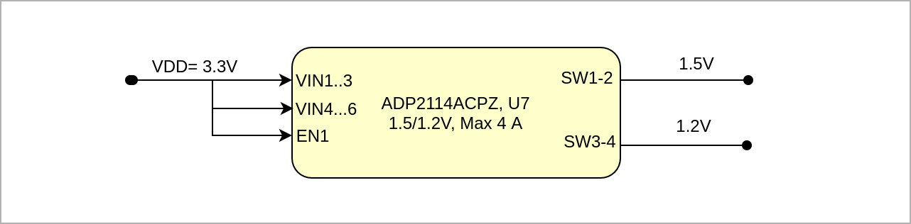
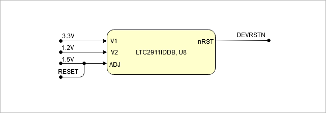
The TEM0005 is equipped with a voltage monitoring IC, U8. Reset Logic Output (nRST) asserts low when any of the V1, V2, or ADJ inputs are below their reset thresholds.
| Scroll Title | ||||||||||||||||||||||||||||
|---|---|---|---|---|---|---|---|---|---|---|---|---|---|---|---|---|---|---|---|---|---|---|---|---|---|---|---|---|
| ||||||||||||||||||||||||||||
|
Power
...
Rails
| Scroll Title | ||||||||
|---|---|---|---|---|---|---|---|---|
| ||||||||
| ||||||||
| diagramName | TEM0005_PWR_PS | |||||||
| simpleViewer | false | width | ||||||
| links | auto | |||||||
| tbstyle | hidden | diagramDisplayName | ||||||
| lbox | true | |||||||
| diagramWidth | 641 | |||||||
| revision | 1 |
| Scroll Only |
|---|
|
Voltage Monitor Circuit
...
| anchor | Figure_PWR_VMC |
|---|---|
| title | Voltage Monitor Circuit |
| Scroll Ignore |
|---|
Create DrawIO object here: Attention if you copy from other page, objects are only linked. |
| Scroll Only |
|---|
image link to the generate DrawIO PNG file of this page. This is a workaround until scroll pdf export bug is fixed |
|
Bank Voltages
...
| Scroll Title | |||||||||||||||||||||||||||
|---|---|---|---|---|---|---|---|---|---|---|---|---|---|---|---|---|---|---|---|---|---|---|---|---|---|---|---|
| |||||||||||||||||||||||||||
Power Rail Name | B2B Connector JM1 Pin B2B Connector JM2 Pin B2B Connector JM3 Pin
|
Bank Voltages
| |||||||||||||||||||||||||||||||
| Scroll Title | |||||||||||||||||||||||||||||||
|---|---|---|---|---|---|---|---|---|---|---|---|---|---|---|---|---|---|---|---|---|---|---|---|---|---|---|---|---|---|---|---|
| |||||||||||||||||||||||||||||||
| Scroll Table Layout | | ||||||||||||||||||||||||||||||
| orientation | portrait | ||||||||||||||||||||||||||||||
| sortDirection | ASC | ||||||||||||||||||||||||||||||
| repeatTableHeaders | default | style | widths | ||||||||||||||||||||||||||||
| sortByColumn | 1 | ||||||||||||||||||||||||||||||
| sortEnabled | false | ||||||||||||||||||||||||||||||
| cellHighlighting | true |
Bank | Schematic Name | Voltage | Notes
|---|---|
Board to Board Connectors
| Page properties | ||||||
|---|---|---|---|---|---|---|
| ||||||
|
| Include Page | ||||
|---|---|---|---|---|
|
Technical Specifications
Absolute Maximum Ratings
| Scroll Title | ||||||||||||||||||||||||||||||||||||||||
|---|---|---|---|---|---|---|---|---|---|---|---|---|---|---|---|---|---|---|---|---|---|---|---|---|---|---|---|---|---|---|---|---|---|---|---|---|---|---|---|---|
| ||||||||||||||||||||||||||||||||||||||||
|
Recommended Operating Conditions
Operating temperature range depends also on customer design and cooling solution. Please contact us for options.
| Scroll Title | |||||||||||||||||||||||||||||||||||||||||||||||||
|---|---|---|---|---|---|---|---|---|---|---|---|---|---|---|---|---|---|---|---|---|---|---|---|---|---|---|---|---|---|---|---|---|---|---|---|---|---|---|---|---|---|---|---|---|---|---|---|---|---|
| |||||||||||||||||||||||||||||||||||||||||||||||||
|
Physical Dimensions
Module size: ?? 56 mm × ?? 31 mm. Please download the assembly diagram for exact numbers.
Mating height with standard connectors: ? 4 mm.
PCB thickness: ?? 1.6 mm.
| Page properties | ||||
|---|---|---|---|---|
| ||||
In 'Physical Dimension' section, top and bottom view of module must be inserted, information regarding physical dimensions can be obtained through webpage for product in Shop.Trenz, (Download> Documents> Assembly part) for every SoM. For Example: for Module TE0728, Physical Dimension information can be captured by snipping tools from the link below:
|
...
| Scroll Title | |||||||||||||||||||||||||||||||||||||||||||
|---|---|---|---|---|---|---|---|---|---|---|---|---|---|---|---|---|---|---|---|---|---|---|---|---|---|---|---|---|---|---|---|---|---|---|---|---|---|---|---|---|---|---|---|
| |||||||||||||||||||||||||||||||||||||||||||
|
Currently Offered Variants
| Page properties | ||||
|---|---|---|---|---|
| ||||
Set correct link to the shop page overview table of the product on English and German. Example for TE0706: ENG Page: https://shop.trenz-electronic.de/en/search?sSearch=TE0706 DEU Page: https://shop.trenz-electronic.de/de/search?sSearch=TE0706 |
...
| Scroll Title | ||||||||||||||||||||||
|---|---|---|---|---|---|---|---|---|---|---|---|---|---|---|---|---|---|---|---|---|---|---|
| ||||||||||||||||||||||
| ||||||||||||||||||||||
Revision History
Hardware Revision History
| Page properties | ||||
|---|---|---|---|---|
| ||||
Set correct links to download arrier, e.g. TE0706 REV02: TE0706-02 -> https://shop.trenz-electronic.de/Download/?path=Trenz_Electronic/Modules_and_Module_Carriers/4x5/4x5_Carriers/TE0706/REV02/Documents Note:
|
...
| Scroll Title | ||||||||||||||||||||||||||||||
|---|---|---|---|---|---|---|---|---|---|---|---|---|---|---|---|---|---|---|---|---|---|---|---|---|---|---|---|---|---|---|
| ||||||||||||||||||||||||||||||
|
Hardware revision number can be found on the PCB board together with the module model number separated by the dash.
| Scroll Title | ||||||||||||||||||||||||||||
|---|---|---|---|---|---|---|---|---|---|---|---|---|---|---|---|---|---|---|---|---|---|---|---|---|---|---|---|---|
| ||||||||||||||||||||||||||||
|
Document Change History
| Page properties | ||||
|---|---|---|---|---|
| ||||
|
...
| Scroll Title | ||||||||||||||||||||||||||||||||||||||||||||||||||||||||||||||||
|---|---|---|---|---|---|---|---|---|---|---|---|---|---|---|---|---|---|---|---|---|---|---|---|---|---|---|---|---|---|---|---|---|---|---|---|---|---|---|---|---|---|---|---|---|---|---|---|---|---|---|---|---|---|---|---|---|---|---|---|---|---|---|---|---|
| ||||||||||||||||||||||||||||||||||||||||||||||||||||||||||||||||
|
Disclaimer
| Include Page | ||||
|---|---|---|---|---|
|
...
Overview
Content Tools