...
| Scroll Title |
|---|
| anchor | Table_SIP_USB |
|---|
| title | General overview of the USB PHY signals |
|---|
|
| Scroll Table Layout |
|---|
| orientation | portrait |
|---|
| sortDirection | ASC |
|---|
| repeatTableHeaders | default |
|---|
| style | |
|---|
| widths | |
|---|
| sortByColumn | 1 |
|---|
| sortEnabled | false |
|---|
| cellHighlighting | true |
|---|
|
| PHY Pin | ZYNQ Pin | B2B Name | Notes |
|---|
| ULPI | MIO52..63 | - | Zynq USB0 MIO pins are connected to the USB PHY. | | REFCLK | - | - | 52.000000 MHz from on-board oscillator (U14). | | REFSEL[0..2] | - | - | Reference clock frequency select, all set to GND selects 52.000000 MHz. | | RESETB | MIO25 | - | Active low reset. | | CLKOUT | MIO52 | - | Connected to 1.8V, selects reference clock operation mode. | | DP, DM | - | OTG_D_P, OTG_D_N | USB data lines routed to B2B connector JM3 pins 47 and 49. | | CPEN | - | VBUS_V_EN | External USB power switch active high enable signal, routed to JM3 pin 17. | | VBUS | - | USB_VBUS | Connect to USB VBUS via a series of resistors, see reference schematics, routed to JM3 pin 55. | | ID | - | OTG_ID | For an A-device connect to ground, for a B-device left floating. routed from JM3 pin 23. |
|
...
I2C Interface
On-board I2C devices are connected to MIO38 (SCL) and MIO39 (SDA) which are configured as I2C0 by default. Addresses for on-board I2C slave devices are listed in the table below:
| Scroll Title |
|---|
| anchor | Table_SIP_I2C |
|---|
| title | Address table of the I2C bus slave devices |
|---|
|
| Scroll Table Layout |
|---|
| orientation | portrait |
|---|
| sortDirection | ASC |
|---|
| repeatTableHeaders | default |
|---|
| style | |
|---|
| widths | |
|---|
| sortByColumn | 1 |
|---|
| sortEnabled | false |
|---|
| cellHighlighting | true |
|---|
|
| I2C Device | I2C Address | Notes |
|---|
Si5338A PLL | 0x70 | - | | EEPROM | 0x50 | - |
|
MIO Pins
| Page properties |
|---|
|
you must fill the table below with group of MIOs which are connected to a specific components or peripherals, you do not have to specify pins in B2B, Just mention which B2B is connected to MIOs. The rest is clear in the Schematic. Example: | MIO Pin | Connected to | B2B | Notes |
|---|
| MIO12...14 | SPI_CS , SPI_DQ0... SPI_DQ3 SPI_SCK | J2 | QSPI |
|
...
| Scroll Title |
|---|
| anchor | Table_OBP |
|---|
| title | On board peripherals |
|---|
|
| Scroll Table Layout |
|---|
| orientation | portrait |
|---|
| sortDirection | ASC |
|---|
| repeatTableHeaders | default |
|---|
| style | |
|---|
| widths | |
|---|
| sortByColumn | 1 |
|---|
| sortEnabled | false |
|---|
| cellHighlighting | true |
|---|
|
| Chip/Interface | Designator | Notes |
|---|
|
Quad SPI Flash Memory
| Page properties |
|---|
|
Notes : Minimum and Maximum density of quad SPI flash must be mentioned for other assembly options. |
Quad SPI Flash Memory
The TE0821 is equipped with dual Flash Memory, U7, U17. Two quad SPI compatible serial bus flash MT25QU512ABB8E12-0SIT memory chips are provided for FPGA configuration file storage. After configuration completes the remaining free memory can be used for application data storage. All four SPI data lines are connected to the FPGA allowing x1, x2 or x4 data bus widths to be used. The maximum data transfer rate depends on the bus width and clock frequency.
| Page properties |
|---|
|
Notes : Minimum and Maximum density of quad SPI flash must be mentioned for other assembly options. |
| Scroll Title |
|---|
| anchor | Table_OBP_SPI |
|---|
| title | Quad SPI interface MIOs and pins |
|---|
|
| Scroll Table Layout |
|---|
| orientation | portrait |
|---|
| sortDirection | ASC |
|---|
| repeatTableHeaders | default |
|---|
| style | |
|---|
| widths | |
|---|
|
|
| Scroll Title |
|---|
| anchor | Table_OBP_SPI |
|---|
| title | Quad SPI interface MIOs and pins |
|---|
|
| Scroll Table Layout |
|---|
| orientation | portrait |
|---|
| sortDirection | ASC |
|---|
| repeatTableHeaders | default |
|---|
| style | widths | sortByColumn | 1 |
|---|
| sortEnabled | false |
|---|
| cellHighlighting | true |
|---|
|
| MIO Pin | Schematic | U?? Pin | Notes |
|---|
|
...
| ?? Pin | Notes |
|---|
| nCS | MIO5 | MIO7 |
| | CLK | MIO0 | MIO12 |
| | DI/IO0 | MIO4 | MIO8 |
| | DO/IO1 | MIO1 | MIO9 |
| | nHOLD/IO3 | MIO3 | MIO11 |
| | WP/IO2 | MIO2 | MIO10 |
|
|
EEPROM
There is a 2Kb EEPROM provided on the module TE0821.
| Scroll Title |
|---|
| anchor | Table_OBP_EEP |
|---|
| title | I2C EEPROM interface MIOs and pins |
|---|
|
| Scroll Table Layout |
|---|
| orientation | portrait |
|---|
| sortDirection | ASC |
|---|
| repeatTableHeaders | default |
|---|
| style | |
|---|
| widths | |
|---|
| sortByColumn | 1 |
|---|
| sortEnabled | false |
|---|
| cellHighlighting | true |
|---|
|
| MIO Pin | Schematic | U?? Pin | Notes |
|---|
| MIO39 | I2C_SDA | SDA |
| | MIO38 | I2C_SCL | SCL |
|
|
| Scroll Title |
|---|
| anchor | Table_OBP_I2C_EEPROM |
|---|
| title | I2C address for EEPROM |
|---|
|
| Scroll Table Layout |
|---|
| orientation | portrait |
|---|
| sortDirection | ASC |
|---|
| repeatTableHeaders | default |
|---|
| style | |
|---|
| widths | |
|---|
| sortByColumn | 1 |
|---|
| sortEnabled | false |
|---|
| cellHighlighting | true |
|---|
|
| MIO Pin | I2C Address | Designator | Notes |
|---|
|
|
|
|
|
LEDs
| Scroll Title |
|---|
| anchor | Table_OBP_LED |
|---|
| title | On-board LEDs |
|---|
|
| Scroll Table Layout |
|---|
| orientation | portrait |
|---|
| sortDirection | ASC |
|---|
| repeatTableHeaders | default |
|---|
| style | |
|---|
| widths | |
|---|
| sortByColumn | 1 |
|---|
| sortEnabled | false |
|---|
| cellHighlighting | true |
|---|
|
| Designator | Color | Connected to | Active Level | Note |
|---|
| D1 | Red | DONE | Low |
| | D2 | Green | USR_LED | High |
| | D3 | Red | ERR_OUT | High |
| | D4 | Green | ERR_STATUS | High |
|
|
DDR4 SDRAM
| Page properties |
|---|
|
Notes : Minimum and Maximum density of DDR3 SDRAM must be mentioned for other assembly options. (pay attention to supported address length for DDR3) |
The TE0821 SoM has dual 8 Gb volatile DDR4 SDRAM IC for storing user application code and data.
- Part number: K4A8G165WB-BIRC
- Supply voltage: 1.2V
- Speed: 2400 Mbps
- Temperature: -40 ~ 95 °C
Gigabyte Ethernet
On-board Gigabit Ethernet PHY (U8) is provided with Marvell Alaska 88E1512 IC (U8). The Ethernet PHY RGMII interface is connected to the ZynqMP Ethernet3 PS GEM3. I/O voltage is fixed at 1.8V for HSTL signaling. The reference clock input of the PHY is supplied from an on-board 25.00 MHz oscillator (U11).
| Scroll Title |
|---|
| anchor | Table_OBP_ETH |
|---|
| title | Ethernet PHY to Zynq SoC connections |
|---|
|
| Scroll Table Layout |
|---|
| orientation | portrait |
|---|
| sortDirection | ASC |
|---|
| repeatTableHeaders | default |
|---|
| style | |
|---|
| widths | |
|---|
| sortByColumn | 1 |
|---|
| sortEnabled | false |
|---|
| cellHighlighting | true |
|---|
|
| U8 Pin | Schematic | Connected to | Note |
|---|
| MDIP0...3 | PHY_MDI0...3 | B2B, JM1 |
| | MDC | ETH_MDC | MIO76 |
| | MDIO | ETH_MDIO | MIO77 |
| | S_IN | S_IN | B2B, JM3 |
| | S_OUT | S_OUT | B2B, JM3 |
| | TXD0..3 | ETH_TXD0...3 | MIO65...68 |
| | TX_CTRL | ETH_TXCTL | MIO69 |
| | TX_CLK | ETH_TXCK | MIO64 |
| | RXD0...3 | ETH_RXD0...3 | MIO71...74 |
| | RX_CTRL | ETH_RXCTL | MIO75 |
| | RX_CLK | ETH_RXCK | MIO70 |
| | LED0...2 | PHY_LED0...2 | FPGA Bank 66 |
| | RESETn | ETH_RST | MIO24 |
|
|
Clock Sources
| Scroll Title |
|---|
| anchor | Table_OBP_CLK |
|---|
| title | Osillators |
|---|
|
| Scroll Table Layout |
|---|
| orientation | portrait |
|---|
| sortDirection | ASC |
|---|
| repeatTableHeaders | default |
|---|
| style | |
|---|
| widths | |
|---|
| sortByColumn | 1 |
|---|
| sortEnabled | false |
|---|
| cellHighlighting | true |
|---|
|
| Designator | Description | Frequency | Note |
|---|
| U11 | MEMS Oscillator | 25 MHz |
| | U14 | MEMS Oscillator | 52 MHz |
| | U32 | MEMS Oscillator | 80 MHz |
|
|
USB2.0 Transceiver
Hi-speed USB ULPI PHY (U18) is provided with USB3320 from Microchip. The ULPI interface is connected to the Zynq PS USB0 via MIO52..63, bank 502. The I/O voltage is fixed at 1.8V and PHY reference clock input is supplied from the on-board 52.00 MHz oscillator (U14).
eMMC Flash Memory
eMMC Flash memory device(U6) is connected to the ZynqMP PS MIO bank 500 pins MIO13..MIO23. eMMC chips IS21ES08G-JCLI (FLASH - NAND Speicher-IC (64 Gb x 1) MMC ) is used.
Programmable Clock Generator
There is a Silicon Labs I2C programmable clock generator Si5338A (U10) chip on the module. It's output frequencies can be programmed using the I2C bus address 0x70 or 0x71. Default address is 0x70, IN4/I2C_LSB pin must be set to high for address 0x71.
A 25.00 MHz oscillator is connected to the pin IN3 and is used to generate the output clocks. The oscillator has its output enable pin permanently connected to 1.8V power rail, thus making output frequency available as soon as 1.8V is present. Three of the Si5338 clock outputs are connected to the FPGA. One is connected to a logic bank and the other two are connected to the GTR banks.
Once running, the frequency and other parameters can be changed by programming the device using the I2C bus connected between the FPGA (master) and clock generator (slave). For this, proper I2C bus logic has to be implemented in FPGA.
| Scroll Title |
|---|
| anchor | Table_OBP_EEPPCLK |
|---|
| title | I2C EEPROM interface MIOs and pinsProgrammable Clock Generator Inputs and Outputs |
|---|
|
| Scroll Table Layout |
|---|
| orientation | portrait |
|---|
| sortDirection | ASC |
|---|
| repeatTableHeaders | default | style | widths |
|---|
| sortByColumn | 1 |
|---|
| sortEnabled | false |
|---|
| cellHighlighting | true |
|---|
|
MIO | Schematic | U?? Pin | Notes | |
| Scroll Title |
|---|
| anchor | Table_OBP_I2C_EEPROM |
|---|
| title | I2C address for EEPROM |
|---|
|
| Scroll Table Layout |
|---|
| orientation | portrait |
|---|
| sortDirection | ASC |
|---|
| repeatTableHeaders | default |
|---|
style | widths | | sortByColumn | 1 |
|---|
| sortEnabled | false |
|---|
| cellHighlighting | true |
|---|
| MIO Pin | I2C Address | Designator | Notes |
|---|
...
| Signal | Connected to | Direction | Note |
|---|
IN0..1 | CLK_IN | JM3 | IN |
| | IN2 | CLK_25M | Oscillator, U11 | IN |
| | SCL | I2C_SCL | EEPROM,U25 | INOUT |
| | SDA | I2C_SDA | EEPROM,U25 | INOUT |
| | CLK0 | CLK0 | JM3 | OUT |
| | CLK1 | B505_CLK3 | FPGA Bank 505 | IN |
| | CLK2 | B505_CLK1 | FPGA Bank 505 | IN |
| | CLK3 | CLK3_N |
| IN |
|
|
Power and Power-On Sequence
| Page properties |
|---|
|
In 'Power and Power-on Sequence' section there are three important digrams which must be drawn: - Power on-sequence
- Power distribution
- Voltage monitoring circuit
|
Power Supply
Power supply with minimum current capability of xx A for system startup is recommended.
Power Consumption
| Scroll Title |
|---|
| anchor | Table_OBPPWR_LEDPC |
|---|
| title | On-board LEDsPower Consumption |
|---|
|
| Scroll Table Layout |
|---|
| orientation | portrait |
|---|
| sortDirection | ASC |
|---|
| repeatTableHeaders | default |
|---|
style | widths | | sortByColumn | 1 |
|---|
| sortEnabled | false |
|---|
| cellHighlighting | true |
|---|
|
|
| Designator | Color | Connected to | Active Level | Note |
|---|
DDR3 SDRAM
| Page properties |
|---|
|
Notes : Minimum and Maximum density of DDR3 SDRAM must be mentioned for other assembly options. (pay attention to supported address length for DDR3) |
The TE???? SoM has ??? GByte volatile DDR3 SDRAM IC for storing user application code and data.
- Part number:
- Supply voltage:
- Speed:
- NOR Flash
- Temperature:
...
| | sortDirection | ASC |
|---|
| repeatTableHeaders | default |
|---|
| style | |
|---|
| widths | |
|---|
| sortByColumn | 1 |
|---|
| sortEnabled | false |
|---|
| cellHighlighting | true |
|---|
|
| Power Input Pin | Typical Current |
|---|
| VIN | TBD* |
|
* TBD - To Be Determined
Power Distribution Dependencies
| Scroll Title |
|---|
| anchor | TableFigure_OBPPWR_ETHPD |
|---|
| title | Ethernet PHY to Zynq SoC connectionsPower Distribution |
|---|
|
tablelayoutorientationportraitsortDirection | ASC |
| repeatTableHeaders | default |
|---|
style | widths | | sortByColumn | 1 |
|---|
| sortEnabled | false |
|---|
| cellHighlighting | true |
|---|
| U?? Pin | Signal Name | Connected to | Signal Description | Note |
|---|
...
| |
|---|
| diagramName | TE0823_PWR_PD |
|---|
| simpleViewer | false |
|---|
| width | |
|---|
| links | auto |
|---|
| tbstyle | top |
|---|
| lbox | true |
|---|
| diagramWidth | 641 |
|---|
| revision | 3 |
|---|
|
|
| Scroll Only |
|---|
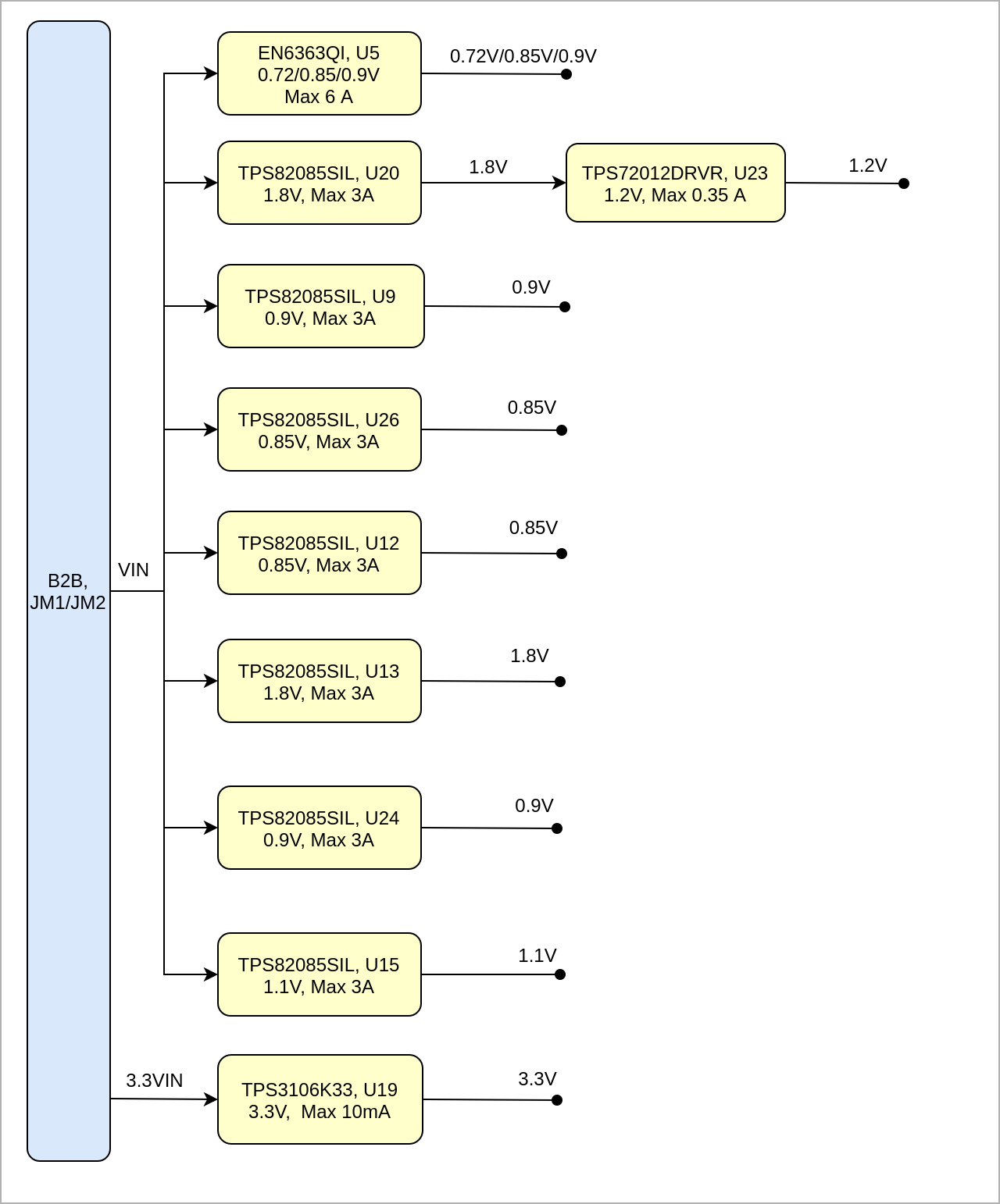 Image Added Image Added
|
|
Power-On Sequence
| Scroll Title |
|---|
| anchor | TableFigure_OBPPWR_CLKPS |
|---|
| title | OsillatorsPower Sequency |
|---|
|
tablelayoutorientationportraitsortDirection | ASC |
| repeatTableHeaders | default |
|---|
style | widths | | sortByColumn | 1 |
|---|
| sortEnabled | false |
|---|
| cellHighlighting | true |
|---|
| Designator | Description | Frequency | Note |
|---|
MHz | MHz | KHz |
Programmable Clock Generator
...
| |
|---|
| diagramName | TE0823_PWR_PS |
|---|
| simpleViewer | false |
|---|
| width | |
|---|
| links | auto |
|---|
| tbstyle | hidden |
|---|
| diagramDisplayName | |
|---|
| lbox | true |
|---|
| diagramWidth | 641 |
|---|
| revision | 3 |
|---|
|
|
| Scroll Only |
|---|
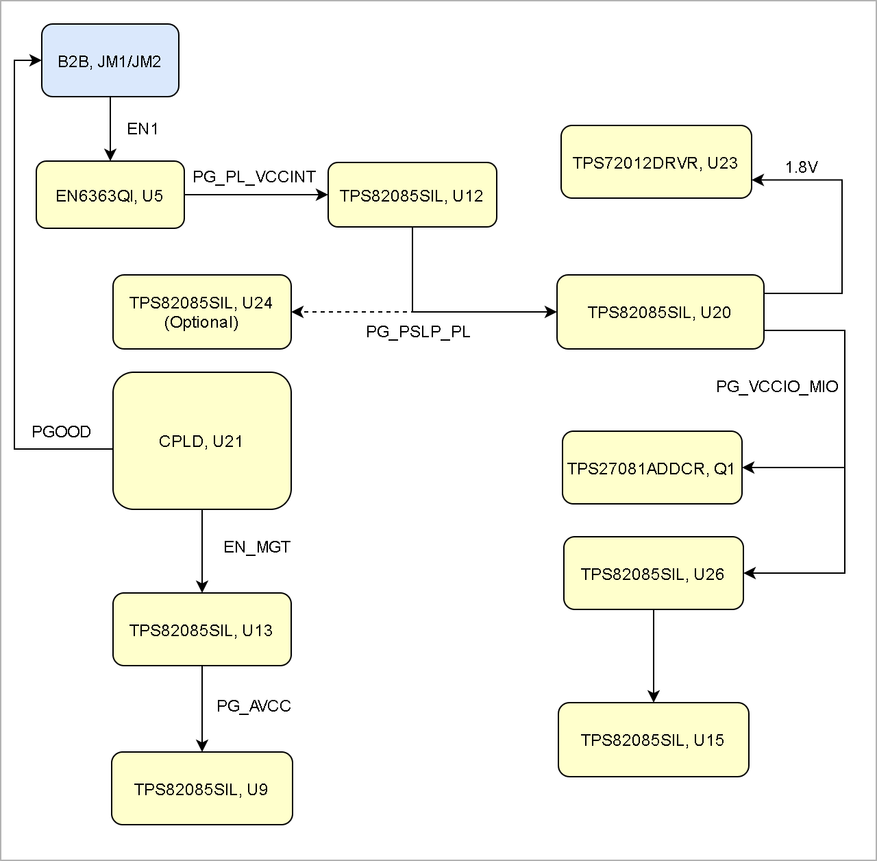 Image Added Image Added
|
|
Power Rails
| Scroll Title |
|---|
| anchor | Table_OBPPWR_PCLKPR |
|---|
| title | Programmable Clock Generator Inputs and OutputsModule power rails. |
|---|
|
| Scroll Table Layout |
|---|
| orientation | portrait |
|---|
| sortDirection | ASC |
|---|
| repeatTableHeaders | default |
|---|
| sortByColumn | 1 |
|---|
| sortEnabled | false |
|---|
| cellHighlighting | true |
|---|
|
|
U?? Pin
| Signal | Connected to | Direction | Note |
|---|
IN0 | IN1 | IN2 | IN3 | XAXB | SCLK | SDA | OUT0 | OUT1 | OUT2 | OUT3 | OUT4 | OUT5 | OUT6 | OUT7 | OUT8/OUT9 |
Power and Power-On Sequence
...
In 'Power and Power-on Sequence' section there are three important digrams which must be drawn:
- Power on-sequence
- Power distribution
- Voltage monitoring circuit
| Note |
|---|
For more information regarding how to draw diagram, Please refer to "Diagram Drawing Guidline" . |
| portrait |
|---|
| sortDirection | ASC |
|---|
| repeatTableHeaders | default |
|---|
| style | |
|---|
| widths | |
|---|
| sortByColumn | 1 |
|---|
| sortEnabled | false |
|---|
| cellHighlighting | true |
|---|
|
| Power Rail Name | B2B Connector JM1 Pin | B2B Connector JM2 Pin | B2B Connector JM3 Pin | Direction | Notes |
|---|
| VIN | 1, 3, 5 | 2, 4, 6, 8 | Input | Supply voltage from the carrier board |
| | 3.3V | - | 10, 12 | Output | Internal 3.3V voltage level |
| | 3.3VIN | 13, 15 | - | Input | Supply voltage from the carrier board |
| | 1.8V | 39 | - | Output | Internal 1.8V voltage level |
| | JTAG VREF | - | 91 | Output | JTAG reference voltage.
Attention: Net name on schematic is "3.3VIN" |
| | VCCO_64 | - | 7, 9 | Input | High performance I/O bank voltage |
| | VCCO_65 | - | 5 | Input | High performance I/O bank voltage |
| | VCCO_66 | 9, 11 | - | Input | High performance I/O bank voltage |
|
|
Bank Voltages
Power Supply
Power supply with minimum current capability of xx A for system startup is recommended.
...
| Scroll Title |
|---|
| anchor | Table_PWR_PCBV |
|---|
| title | Power ConsumptionZynq SoC bank voltages. |
|---|
|
| Scroll Table Layout |
|---|
| orientation | portrait |
|---|
| sortDirection | ASC |
|---|
| repeatTableHeaders | default |
|---|
| style | |
|---|
| widths | |
|---|
| sortByColumn | 1 |
|---|
| sortEnabled | false |
|---|
| cellHighlighting | true |
|---|
|
|
| Power Input Pin | Typical Current |
|---|
| VIN | TBD* |
* TBD - To Be Determined
Power Distribution Dependencies
...
| anchor | Figure_PWR_PD |
|---|
| title | Power Distribution |
|---|
| Schematic Name | | Notes |
|---|
| 24 HD | VCCO_HD24_24 | Variable | Max voltage 3.3V | | 25 HD |
| Variable | Max voltage 3.3V | | 26 HD | VCCO_HD25_26 | Variable | Max voltage 3.3V | | 44 HD | VCCO_HD24_44 | Variable | Max voltage 3.3V | | 65 HP | VCCO_65 | Variable | Max voltage 1.8V | | 66 HP | VCCO_66 | 1.8V |
| | 500 PSMIO | VCCO_PSIO0_500 | 1.8V |
| 501 PSMIO | VCCO_PSIO1_501 | 3.3V |
| | 502 PSMIO | VCCO_PSIO2_502 | 1.8V |
| | 503 PSCONFIG | VCCO_PSIO3_503 | 1.8V |
| | 504 PSDDR | DDR_1V2 | 1.2V |
|
|
Board to Board Connectors
| Page properties |
|---|
|
- This section is optional and only for modules.
use "include page" macro and link to the general B2B connector page of the module series, For example: 6 x 6 SoM LSHM B2B Connectors
| Include Page |
|---|
| PD:6 x 6 SoM LSHM B2B Connectors |
|---|
| PD:6 x 6 SoM LSHM B2B Connectors |
|---|
|
|
| Include Page |
|---|
| PD:4 x 5 SoM LSHM B2B Connectors |
|---|
| PD:4 x 5 SoM LSHM B2B Connectors |
|---|
|
Technical Specifications
Absolute Maximum Ratings
...
| Scroll Only |
|---|
Image Removed |
Power-On Sequence
...
| anchor | Figure_PWR_PS |
|---|
| title | Power Sequency |
|---|
...
| Scroll Only |
|---|
Image Removed |
Power Rails
| Scroll Title |
|---|
| anchor | Table_PWRTS_PRAMR |
|---|
| title | Module power rails.PS absolute maximum ratings |
|---|
|
| Scroll Table Layout |
|---|
| orientation | portrait |
|---|
| sortDirection | ASC |
|---|
| repeatTableHeaders | default |
|---|
| style | |
|---|
| widths | |
|---|
| sortByColumn | 1 |
|---|
| sortEnabled | false |
|---|
| cellHighlighting | true |
|---|
|
|
| Power Rail Name | B2B Connector JM1 Pin | B2B Connector JM2 Pin | B2B Connector JM3 Pin | Direction | Notes |
|---|
Bank Voltages
...
| anchor | Table_PWR_BV |
|---|
| title | Zynq SoC bank voltages. |
|---|
...
...
...
...
| Symbols | Description | Min | Max | Unit |
|---|
VIN supply voltage | -0.3 | 7 | V | See EN6347QI and TPS82085SIL datasheets | | 3.3VIN supply voltage | -0.1 | 3.630 | V | Xilinx DS925 and TPS27082L datasheet | | PS I/O supply voltage, VCCO_PSIO | -0.5 | 3.630 | V | Xilinx document DS925 | | PS I/O input voltage | -0.5 | VCCO_PSIO + 0.55 | V | Xilinx document DS925 | | HP I/O bank supply voltage, VCCO | -0.5 | 2.0 | V | Xilinx document DS925 | | HP I/O bank input voltage | -0.55 | VCCO + 0.55 | V | Xilinx document DS925 | | PS GTR reference clocks absolute input voltage | -0.5 | 1.1 | V | Xilinx document DS925 | | PS GTR absolute input voltage | -0.5 | 1.1 | V | Xilinx document DS925 | Voltage on SC CPLD pins | -0.5 | 3.75 | V | Lattice Semiconductor MachXO2 datasheet | Storage temperature | -40 | +85 | °C | See eMMC datasheet |
|
Recommended Operating Conditions
Operating temperature range depends also on customer design and cooling solution. Please contact us for options.
use "include page" macro and link to the general B2B connector page of the module series,
...
Technical Specifications
Absolute Maximum Ratings
| Scroll Title |
|---|
| anchor | Table_TS_AMRROC |
|---|
| title | PS absolute maximum ratingsRecommended operating conditions. |
|---|
|
| Scroll Table Layout |
|---|
| orientation | portrait |
|---|
| sortDirection | ASC |
|---|
| repeatTableHeaders | default |
|---|
| style | |
|---|
| widths | |
|---|
| sortByColumn | 1 |
|---|
| sortEnabled | false |
|---|
| cellHighlighting | true |
|---|
|
| Symbols | DescriptionUnitV | | Reference Document |
|---|
| VIN supply voltage | 3.3 | 6 |
V | V | V |
Recommended Operating Conditions
Operating temperature range depends also on customer design and cooling solution. Please contact us for options.
| See TPS82085S datasheet | | 3.3VIN supply voltage | 3.3 | 3.465 | V | See LCMXO2-256HC, Xilinx DS925 datasheet | | PS I/O supply voltage, VCCO_PSIO | 1.710 | 3.465 | V | Xilinx document DS925 | | PS I/O input voltage | –0.20 | VCCO_PSIO + 0.20 | V | Xilinx document DS925 | | HP I/O banks supply voltage, VCCO | 0.950 | 1.9 | V | Xilinx document DS925 | | HP I/O banks input voltage | -0.20 | VCCO + 0.20 | V | Xilinx document DS925 | | Voltage on SC CPLD pins | -0.3 | 3.6 | V | Lattice Semiconductor MachXO2 datasheet | | Operating Temperature Range | 0 | 85 | °C | Xilinx document DS925, extended grade Zynq temperarure range |
|
| Scroll Title |
|---|
| anchor | Table_TS_ROC |
|---|
| title | Recommended operating conditions. |
|---|
|
| Scroll Table Layout |
|---|
|
| orientation | portrait |
|---|
| sortDirection | ASC |
|---|
| repeatTableHeaders | default |
|---|
style | widths | | sortByColumn | 1 |
|---|
| sortEnabled | false |
|---|
| cellHighlighting | true |
|---|
| Parameter | Min | Max | Units | Reference Document |
|---|
| V | See ???? datasheets. | V | See Xilinx ???? datasheet. | V | See Xilinx ???? datasheet. | °C | See Xilinx ???? datasheet. | °C | See Xilinx ???? datasheet. |
Physical Dimensions
Module size: 40 mm × 50 mm. Please download the assembly diagram for exact numbers.
Mating height with standard connectors: 8 mm.
...