...
| Scroll Title |
|---|
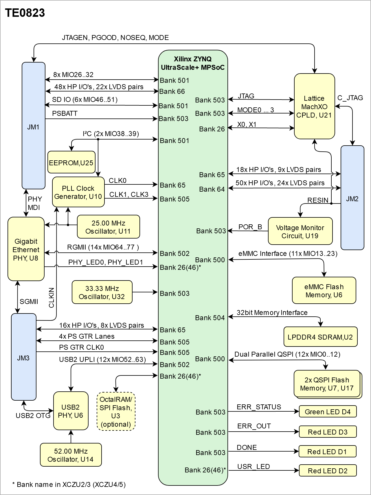
| anchor | Figure_OV_BD |
|---|
| title | TE0823 block diagram |
|---|
|
| Scroll Ignore |
|---|
| draw.io Diagram |
|---|
| border | false |
|---|
| |
|---|
| diagramName | TE0823_OV_BD |
|---|
| simpleViewer | false |
|---|
| width | |
|---|
| links | auto |
|---|
| tbstyle | hidden |
|---|
| diagramDisplayName | |
|---|
| lbox | true |
|---|
| diagramWidth | 641 |
|---|
| revision | 68 |
|---|
|
|
| Scroll Only |
|---|
|
|
Main Components
...
| Scroll Title |
|---|
| anchor | Table_SIP_B2B |
|---|
| title | General PL I/O to B2B connectors information |
|---|
|
| Scroll Table Layout |
|---|
| orientation | portrait |
|---|
| sortDirection | ASC |
|---|
| repeatTableHeaders | default |
|---|
| style | |
|---|
| widths | |
|---|
| sortByColumn | 1 |
|---|
| sortEnabled | false |
|---|
| cellHighlighting | true |
|---|
|
| FPGA Bank | B2B Connector | I/O Signal Count | Voltage Level | Notes |
|
|---|
| 24 | HD | JM2 | 24x I/O, 12x LVDS Pairs | Variable | Max voltage 3.3V | | 25 | HD | JM1 | 24x I/O, 12x LVDS Pairs | Variable | Max voltage 3.3V | | 26 | HD | JM1 | 24x I/O, 12x LVDS Pairs | Variable | Max voltage 3.3V | | 44 | HD | JM2 | 24x I/O, 12x LVDS Pairs | Variable | Max voltage 3.3V | | 65 | HP | JM2 | 18x I/O, 9x LVDS Pairs | Variable | Max voltage 1.8V | 65 | HP | JM3 | 16x I/O, 8x LVDS Pairs | Variable | Max voltage 1.8V | | 505 | GTR | JM3 | 16x I/O, 8x LVDS Pairs | - | 4x lanes | | 505 | GTR CLK | JM3 | 1x Diff Clock | - |
| 501 | MIO | JM1 | 15 I/O | 3.3V |
|
|
...
| Page properties |
|---|
|
Notes : Minimum and Maximum density of DDR3 SDRAM must be mentioned for other assembly options. (pay attention to supported address length for DDR3) |
The TE0821 SoM has dual 8 Gb volatile DDR4 SDRAM IC for storing user application code and data.
- Part number: K4A8G165WB-BIRC
- Supply voltage: 1.2V
- Speed: 2400 Mbps
- Temperature: -40 ~ 95 °C
Gigabyte Ethernet
On-board Gigabit Ethernet PHY (U8) is provided with Marvell Alaska 88E1512 IC (U8). The Ethernet PHY RGMII interface is connected to the ZynqMP Ethernet3 PS GEM3. I/O voltage is fixed at 1.8V for HSTL signaling. The reference clock input of the PHY is supplied from an on-board 25.00 MHz oscillator (U11).
...
| Scroll Title |
|---|
| anchor | Table_OBP_CLK |
|---|
| title | Osillators |
|---|
|
| Scroll Table Layout |
|---|
| orientation | portrait |
|---|
| sortDirection | ASC |
|---|
| repeatTableHeaders | default |
|---|
| style | |
|---|
| widths | |
|---|
| sortByColumn | 1 |
|---|
| sortEnabled | false |
|---|
| cellHighlighting | true |
|---|
|
| Designator | Description | Frequency | Note |
|---|
| U11 | MEMS Oscillator | 25 MHz |
| | U14 | MEMS Oscillator | 52 MHz |
| | U32 | MEMS Oscillator | 80 MHz |
|
|
USB2.0 Transceiver
Hi-speed USB ULPI PHY (U18) is provided with USB3320 from Microchip. The ULPI interface is connected to the Zynq PS USB0 via MIO52..63, bank 502. The I/O voltage is fixed at 1.8V and PHY reference clock input is supplied from the on-board 52.00 MHz oscillator (U14).
eMMC Flash Memory
eMMC Flash memory device(U6) is connected to the ZynqMP PS MIO bank 500 pins MIO13..MIO23. eMMC chips IS21ES08G-JCLI (FLASH - NAND Speicher-IC (64 Gb x 1) MMC ) is used.
Programmable Clock Generator
There is a Silicon Labs I2C programmable clock generator Si5338A (U10) chip on the module. It's output frequencies can be programmed using the I2C bus address 0x70 or 0x71. Default address is 0x70, IN4/I2C_LSB pin must be set to high for address 0x71.
A 25.00 MHz oscillator is connected to the pin IN3 and is used to generate the output clocks. The oscillator has its output enable pin permanently connected to 1.8V power rail, thus making output frequency available as soon as 1.8V is present. Three of the Si5338 clock outputs are connected to the FPGA. One is connected to a logic bank and the other two are connected to the GTR banks.
Once running, the frequency and other parameters can be changed by programming the device using the I2C bus connected between the FPGA (master) and clock generator (slave). For this, proper I2C bus logic has to be implemented in FPGA.
| Scroll Title |
|---|
| anchor | Table_OBP_PCLK |
|---|
| title | Programmable Clock Generator Inputs and Outputs |
|---|
|
| Scroll Table Layout |
|---|
| orientation | portrait |
|---|
| sortDirection | ASC |
|---|
| repeatTableHeaders | default |
|---|
| sortByColumn | 1 |
|---|
| sortEnabled | false |
|---|
| cellHighlighting | true |
|---|
|
U25 Pin
| Signal | Connected to | Direction | Note |
|---|
IN0..1 | CLK_IN | JM3 | IN |
| | IN2 | CLK_25M | Oscillator, U11 | IN |
| | SCL | I2C_SCL | EEPROM,U25 | INOUT |
| | SDA | I2C_SDA | EEPROM,U25 | INOUT |
| | CLK0 | CLK0 | JM3 | OUT |
| | CLK1 | B505_CLK3 | FPGA Bank 505 | IN |
| | CLK2 | B505_CLK1 | FPGA Bank 505 | IN |
| | CLK3 | CLK3_N |
| IN |
|
|
...
| Scroll Title |
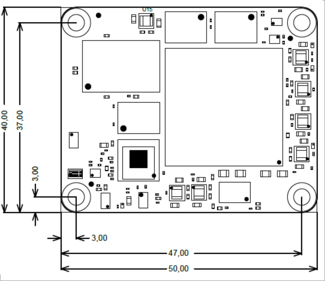
|---|
| anchor | Figure_TS_PD |
|---|
| title | Physical Dimension |
|---|
|
| Scroll Ignore |
|---|
| draw.io Diagram |
|---|
| border | false |
|---|
| |
|---|
| diagramName | TE0823_TS_PD |
|---|
| simpleViewer | false |
|---|
| width | |
|---|
| links | auto |
|---|
| tbstyle | hidden |
|---|
| diagramDisplayName | |
|---|
| lbox | true |
|---|
| diagramWidth | 641542 |
|---|
| revision | 23 |
|---|
|
|
| Scroll Only |
|---|
| scroll-pdf | true |
|---|
| scroll-office | true |
|---|
| scroll-chm | true |
|---|
| scroll-docbook | true |
|---|
| scroll-eclipsehelp | true |
|---|
| scroll-epub | true |
|---|
| scroll-html | true |
|---|
| 
|
|
...
| Scroll Title |
|---|
| anchor | Figure_RV_HRN |
|---|
| title | Board hardware revision number. |
|---|
|
| Scroll Ignore |
|---|
| draw.io Diagram |
|---|
| border | false |
|---|
| |
|---|
| diagramName | TE0823_RV_HRN |
|---|
| simpleViewer | false |
|---|
| width | |
|---|
| links | auto |
|---|
| tbstyle | hidden |
|---|
| diagramDisplayName | |
|---|
| lbox | true |
|---|
| diagramWidth | 254170 |
|---|
| revision | 12 |
|---|
|
|
| Scroll Only |
|---|
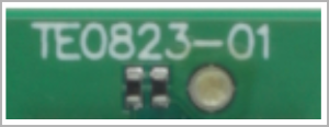 Image Modified Image Modified
|
|
Document Change History
...