...
| Scroll Title |
|---|
| anchor | Figure_OV_BD |
|---|
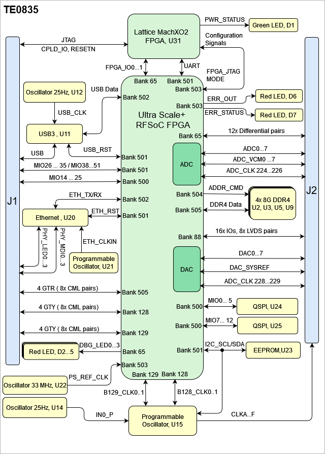
| title | TE0835 block diagram |
|---|
|
| Scroll Ignore |
|---|
| draw.io Diagram |
|---|
| border | false |
|---|
| viewerToolbar | true |
|---|
| |
|---|
| fitWindow | false |
|---|
| diagramDisplayName | |
|---|
| lbox | true |
|---|
| revision | 78 |
|---|
| diagramName | TE0835_OV_BD |
|---|
| simpleViewer | false |
|---|
| width | |
|---|
| links | auto |
|---|
| tbstyle | hidden |
|---|
| diagramWidth | 641640 |
|---|
|
|
| Scroll Only |
|---|
|
|
Main Components
...
| Scroll Title |
|---|
| anchor | Table_OV_BP |
|---|
| title | Boot process. |
|---|
|
| Scroll Table Layout |
|---|
| orientation | portrait |
|---|
| sortDirection | ASC |
|---|
| repeatTableHeaders | default |
|---|
| style | |
|---|
| widths | |
|---|
| sortByColumn | 1 |
|---|
| sortEnabled | false |
|---|
| cellHighlighting | true |
|---|
|
MODE[0:3] | Boot Mode | Pin Location | Note |
|---|
0000 | PS_JTAG | JTAG | PSJTAG Interface | 0001 | Quad SPI (24b) | MIO0...12 | QSPI 24bit addressing | 0010 | Quad SPI (32b) | MIO0...12 | QSPI 32bit addressing | 0011 | SD0 2.0 | MIO13...25 | SD 2.0 | 0100 | NAND | MIO9...25 | Requires 8 bit data bus width | | 0101 | SD1 2.0 | MIO31...51 | SD 2.0 | 0110 | eMMC | MIO13...22 | eMMC version 4.5 at 1.8 V | | 0111 | USB2.0 | MIO52...63 | Only USB2.0 | 1000 | PJTAG | MIO26...29PJTAG Connection 0 0ption | 1001 | PJTAG | MIO12...15 | PJTAG Connection 1 0ption | | 1110 | SD1 LS 3.0 | MIO39...51 | SD 3.0 with complaint voltage level shifter |
|
...
| Scroll Title |
|---|
| anchor | Table_SIP_B2B |
|---|
| title | General PL I/O to B2B connectors information |
|---|
|
| Scroll Table Layout |
|---|
| orientation | portrait |
|---|
| sortDirection | ASC |
|---|
| repeatTableHeaders | default |
|---|
| style | |
|---|
| widths | |
|---|
| sortByColumn | 1 |
|---|
| sortEnabled | false |
|---|
| cellHighlighting | true |
|---|
|
| FPGA Bank | B2B Connector | Number of I/Os | Voltage Level | Notes |
|---|
| Bank 500 | J1 | 12x Single Ended | 1.8V | MIO14...25 | | Bank 501 | J1 | 20x Single Ended | 1.8V | MIO26...51 | | Bank 505 | J1 | 18x Single Ended, 9x Differential pairs | 0.85V | EXT_CLKIN_PSMGT, RX/TX0...3 | | Bank 128 | J1 | 18x Single Ended, 9x Differential pairs | 0.9V | B128_CLK, RX/TX0...3 | | Bank 129 | J1 | 18x Single Ended, 9x Differential pairs | 0.9V | B129_CLK, RX/TX0...3 | | Bank 65 | J2 | 24x Single Ended, 12x Differential pairs | 1.8V |
| | Bank 88 | J2 | 16x Single Ended, 8x Differential pairs | 3.3V |
| HD_B88 | | ADC | J2 | 16x Single Ended, 8x Differential pairs 4x Differential Clocks | Variable |
| | DAC | J2 | 16x Single Ended, 8x Differential pairs 3x Differential Clocks | Variable |
HD_B88
|
JTAG Interface
JTAG access to the TE0835 is through B2B connector JM1.
...
| Scroll Title |
|---|
| anchor | Table_OBP_PCLK |
|---|
| title | Programmable Clock Generator Inputs and Outputs |
|---|
|
| Scroll Table Layout |
|---|
| orientation | portrait |
|---|
| sortDirection | ASC |
|---|
| repeatTableHeaders | default |
|---|
| sortByColumn | 1 |
|---|
| sortEnabled | false |
|---|
| cellHighlighting | true |
|---|
|
U15 Pin
| Signal | Connected to | Direction | Note |
|---|
IN0 | IN0_P | Oscillator, U14 | Input |
| | IN1 | - | N.C | - |
| | IN2 | EXT_CLK_IN1 | B2B,J2 | Input |
| | IN3 | - | N.C |
|
| nRST | PLL_RSTN | FPGA Bank 65,U1 | Input |
| | SCL | MIO32_I2C1_SCL | Pin Header, J3 | Input | I2C | | SDA | MIO33_I2C1_SDA | Pin Header, J3 | Input | OUT0...5 | CLKA...F | I2C | | OUT0 | CLKC | B2B,J2 | Output | Differential Clock | | OUT1 | CLKB | B2B,J2 | Output | Differential Clock | | OUT2 | CLKA | B2B,J2 | Output | Differential Clock | | OUT3 | CLKD | B2B,J2 | Output | Differential Clock | | OUT4 | CLKE | B2B,J2 | Output | Differential Clock | | OUT5 | CLKF | B2B,J2 | Output | 6x Differential | ClocksClock | | OUT6 | B128_CLK0 | FPGA Bank 128,U1 | Output |
| | OUT7 | B129_CLK0 | FPGA Bank 129,U1 | Output |
| | OUT8 | CLK8 | FPGA Bank 65,U1 | Output |
| | OUT9 | PSMGT_100MHZ | FPGA Bank 505,U1 | Output |
| | OUT9A | CLK0A_100MHZ | B2B, J1 | Output |
|
|
...
| Scroll Title |
|---|
| anchor | Figure_PWR_PS |
|---|
| title | Power Sequency |
|---|
|
| Scroll Ignore |
|---|
| draw.io Diagram |
|---|
| border | false |
|---|
| viewerToolbar | true |
|---|
| |
|---|
| fitWindow | false |
|---|
| diagramDisplayName | |
|---|
| lbox | true |
|---|
| revision | 7 |
|---|
| diagramName | TE0835_PWR_PS |
|---|
| simpleViewer | false |
|---|
| width | |
|---|
| links | auto |
|---|
| tbstyle | hidden |
|---|
| diagramWidth | 641 |
|---|
|
|
| Scroll Only |
|---|
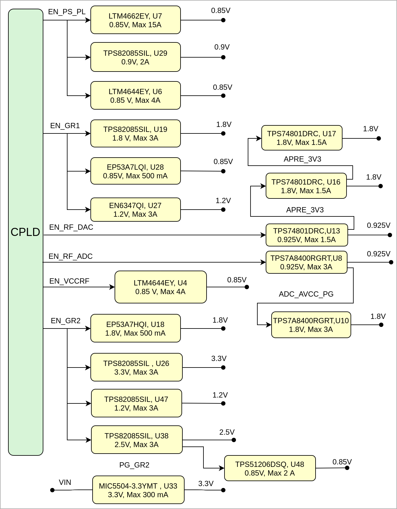 Image Modified Image Modified
|
|
Power Rails
...
| Scroll Title |
|---|
| anchor | Table_TS_AMR |
|---|
| title | PS absolute maximum ratings |
|---|
|
| Scroll Table Layout |
|---|
| orientation | portrait |
|---|
| sortDirection | ASC |
|---|
| repeatTableHeaders | default |
|---|
| style | |
|---|
| widths | |
|---|
| sortByColumn | 1 |
|---|
| sortEnabled | false |
|---|
| cellHighlighting | true |
|---|
|
| Symbols | Description | Min | Max | Unit |
|---|
| VIN | Input Supply Voltage | 0 | 5 | V | | T_STG | Storage Temperature | -40 | 10095 | °C |
|
Recommended Operating Conditions
...
| Scroll Title |
|---|
| anchor | Table_TS_ROC |
|---|
| title | Recommended operating conditions. |
|---|
|
| Scroll Table Layout |
|---|
| orientation | portrait |
|---|
| sortDirection | ASC |
|---|
| repeatTableHeaders | default |
|---|
| style | |
|---|
| widths | |
|---|
| sortByColumn | 1 |
|---|
| sortEnabled | false |
|---|
| cellHighlighting | true |
|---|
|
| Parameter | Min | Max | Units | Reference Document |
|---|
| VIN | 4.5 | 5.5 | V | See Schematic. | | T_OPR | 0 | 85 | °C | See Xilinx XCZU25DR Datasheet see Samsung DDR4 Datasheetsee USB3320 Datasheet |
|
Physical Dimensions
...
| Scroll Title |
|---|
| anchor | Table_RH_HRH |
|---|
| title | Hardware Revision History |
|---|
|
| Scroll Table Layout |
|---|
| orientation | portrait |
|---|
| sortDirection | ASC |
|---|
| repeatTableHeaders | default |
|---|
| style | |
|---|
| widths | |
|---|
| sortByColumn | 1 |
|---|
| sortEnabled | false |
|---|
| cellHighlighting | true |
|---|
|
| Date | Revision | Changes | Documentation Link |
|---|
| 2019-11-05 | REV01 | Initial Release | REV01 |
|
Hardware revision number can be found on the PCB board together with the module model number separated by the dash.
...