| Scroll Table Layout |
|---|
| orientation | portrait |
|---|
| sortDirection | ASC |
|---|
| repeatTableHeaders | default |
|---|
| style | |
|---|
| widths | |
|---|
| sortByColumn | 1 |
|---|
| sortEnabled | false |
|---|
| cellHighlighting | true |
|---|
|
| Power Rail Name | B2B Connector JM1 Pin | B2B Connector JM2 Pin | B2B Connector JM3 Pin | Direction | Notes |
|---|
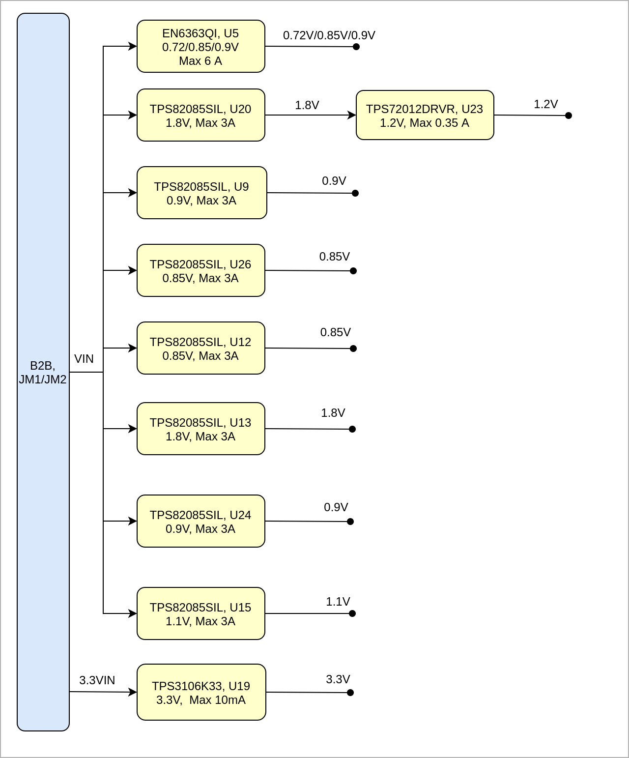
| VIN | 1, 3, 5 | 2, 4, 6, 8 | Input | Supply voltage from the carrier board |
| | 3.3V | - | 10, 12 | Output | Internal 3.3V voltage level |
| | 3.3VIN | 13, 15 | - | Input | Supply voltage from the carrier board |
| | 1.8V | 39 | - | Output | Internal 1.8V voltage level |
| | JTAG VREF | - | 91 | Output | JTAG reference voltage.
Attention: Net name on schematic is "3.3VIN" |
| | VCCO_64 | - | 7, 9 | Input | High performance I/O bank voltage |
| | VCCO_65 | - | 5 | Input | High performance I/O bank voltage |
| | VCCO_66 | 9, 11 | - | Input | High performance I/O bank voltage |
|
|