...
Overview
The Trenz Electronic TE0xxx-xx ... is an industrial-grade ... module ... based on Xilinx ...TEMB0005 is a carrier for the module TEM00005. The carrier is equipped with a LAN socket, a FTDI JTAG/UART to USB2.0 solution, three low speed and one high speed CRUVI B2B Connectors, a PMod Connector.
Refer to http://trenz.org/temb0005-info for the current online version of this manual and other available documentation.
...
| Page properties |
|---|
|
Note:
'description: Important components and connector or other Features of the module
→ please sort and indicate assembly options Key Features' must be split into 6 main groups for modules and mainboards: - SoC/FPGA
- Package: SFVC784
- Device: ZU2...ZU5*
- Engine: CG, EG, EV*
- Speed: -1LI, -2LE,*, **
- Temperature: I, E,*, **
- RAM/Storage
- Low Power DDR4 on PS
- Data width: 32bit
- Size: def. 2GB*
- Speed:***
- eMMC
- Data width: 8Bit
- size: def. 8GB *
- QSPI boot Flash in dual parallel mode (size depends on assembly version)
- Data width: 8bit
- size: def. 128MB *
- HyperRAM/Flash (optional, default not assembled)
- MAC address serial EEPROM with EUI-48™ node identity (Microchip 24AA025E48)
- On Board
- Lattice LCMXO2
- PLL SI5338
- Gigabit Ethernet transceiver PHY (Marvell Alaska 88E1512)
- Hi-speed USB2 ULPI transceiver with full OTG support (Microchip USB3320C)
- Interface
- 132 x HP PL I/Os (3 banks)
- ETH
- USB
- 4 GTR (for USB3, Sata, PCIe, DP)
- MIO for UART
- MIO for SD
- MIO for PJTAG
- JTAG
- Ctrl
- Power
- 3.3V-5V Main Input
- 3.3V Controller Input
- Variable Bank IO Power Input
- Dimension
- Notes
- * depends on assembly version
- ** also non low power assembly options possible
- *** depends on used U+ Zynq and DDR4 combination
Key Features' must be split into 6 main groups for carrier: - Modules
- TE0808, TE807, TE0803,...
- RAM/Storage
- On Board
- Interface
- E.g. ETH, USB, B2B, Display port
- Power
- E.g. Input supply voltage
- Dimension
|
- <Replace for module use "SoC/FPGA" for Carrier "Modules">
- RAM/Storage
- On Board
- Interface
- Power
- Dimension
- Notes
Block Diagram
- FT2232H FTDI
- 4x User LEDs
- 2x Push Buttons
- 2x MEMS Oscillators
- Interface
- 1x Samtec Razor Beam (SS5) B2B Connector
- 1x Samtec Razor Beam (SS4) High Speed CRUVI Connector
- 3x Samtec Low Speed CRUVI Connectors
- 1x PMod SMD (2x6) Connector
- 1x SMD Header (1x6)
- 1x RJ45 LAN Socket
- 1x Micro USB2.0 Connector
- Power
- Dimension
- Notes
Block Diagram
| Page properties |
|---|
| Page properties |
|---|
|
add drawIO object here.
|
...
| Scroll Title |
|---|
| anchor | Figure_OV_BD |
|---|
| title | TEMB0005 block diagram |
|---|
|
| Scroll Ignore |
|---|
| draw.io Diagram |
|---|
| border | false |
|---|
| |
|---|
| diagramName | TEMB0005_OV_BD |
|---|
| simpleViewer | false |
|---|
| width | 639 |
|---|
| links | auto |
|---|
| tbstyle | hidden |
|---|
| diagramDisplayName | |
|---|
| lbox | true |
|---|
| diagramWidth | 641640 |
|---|
| revision | 111 |
|---|
|
|
| Scroll Only |
|---|

|
|
Main Components
...
| Scroll Title |
|---|
| anchor | Figure_OV_MC |
|---|
| title | TEMB0005 main components |
|---|
|
| Scroll Ignore |
|---|
| draw.io Diagram |
|---|
| border | false |
|---|
| |
|---|
| diagramName | TEMB0005_OV_MC |
|---|
| simpleViewer | false |
|---|
| width | 639 |
|---|
| links | auto |
|---|
| tbstyle | hidden |
|---|
| diagramDisplayName | |
|---|
| lbox | true |
|---|
| diagramWidth | 641 |
|---|
| revision | 17 |
|---|
|
|
| Scroll Only |
|---|
|
|
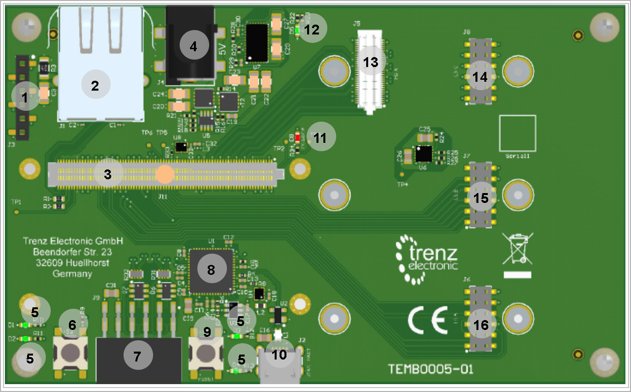
- SMD Header 6x1, J3
- RJ45 LAN Socket, J1
- B2B Connector, J11
- Barrel Jack, J4
- Green LEDs, D1
- ...
- ...
- ...
Initial Delivery State
- 4
- User Push Button, S2
- PMod 2x6 SMD Host Socket, J9
- FT2232H FTDI, U1
- Reset Push Button, S1
- Micro USB2.0 Socket, J2
- Red LED (PG_DCDC), D8
- Green LED (5VIN), D5
- High Speed CRUVI Connectors, J5
- Low Speed CRUVI Connectors, J8
- Low Speed CRUVI Connectors, J7
- Low Speed CRUVI Connectors, J6
Initial Delivery State
| Page properties |
|---|
| Page properties |
|---|
|
Notes : Only components like EEPROM, QSPI flash can be initialized by default at manufacture. If there is no components which might have initial data ( possible on carrier) you must keep the table empty |
...
| Scroll Title |
|---|
| anchor | Table_OV_IDS |
|---|
| title | Initial delivery state of programmable devices on the module |
|---|
|
| Scroll Table Layout |
|---|
| orientation | portrait |
|---|
| sortDirection | ASC |
|---|
| repeatTableHeaders | default |
|---|
| style | |
|---|
| widths | |
|---|
| sortByColumn | 1 |
|---|
| sortEnabled | false |
|---|
| cellHighlighting | true |
|---|
|
Storage device name | Content | Notes |
|---|
| EEPROM | Quad SPI Flash | Programmed | FTDI Confirguration | EEPROM | System Controller CPLD |
|
Configuration Signals
| Page properties |
|---|
|
- Overview of Boot Mode, Reset, Enables.
|
...
| Scroll Title |
|---|
| anchor | Table_OV_BPRST |
|---|
| title | Boot Reset process. |
|---|
|
| Scroll Table Layout |
|---|
| orientation | portrait |
|---|
| sortDirection | ASC |
|---|
| repeatTableHeaders | default |
|---|
| style | |
|---|
| widths | |
|---|
| sortByColumn | 1 |
|---|
| sortEnabled | false |
|---|
| cellHighlighting | true |
|---|
|
|
| Scroll Title |
|---|
| anchor | Table_OV_RST |
|---|
| title | Reset process. |
|---|
|
| Scroll Table Layout |
|---|
| orientation | portrait |
|---|
| sortDirection | ASC |
|---|
| repeatTableHeaders | default |
|---|
style | widths | | sortByColumn | 1 |
|---|
| sortEnabled | false |
|---|
| cellHighlighting | true |
|---|
Signal | B2B | I/O | Note |
|---|
| B2B | Connected to | Note |
|---|
| M_RESET | J11- 11 | Push Button, S1 | Module Reset | | EN_VADJ | J11-110 | DCDC, U6 | pull-down, input from module | | SEL_VADJ | J11-108 | DCDC, U6 | pull-up, input from module.
'low' → 1.8V,
'high'→ 2.5V |
|
Signals, Interfaces and Pins
...
Board to Board (B2B) I/Os
FPGA bank number and number of I/O signals connected to the B2B connector:The carrier TEMB0005 is equipped with a Samtec (SS4) B2B Connector. More information in the following table.
| Scroll Title |
|---|
| anchor | Table_SIP_B2B |
|---|
| title | General PL I/O to B2B B2B connectors information |
|---|
|
| Scroll Table Layout |
|---|
| orientation | portrait |
|---|
| sortDirection | ASC |
|---|
| repeatTableHeaders | default |
|---|
| style | |
|---|
| widths | |
|---|
| sortByColumn | 1 |
|---|
| sortEnabled | false |
|---|
| cellHighlighting | true |
|---|
|
FPGA BankB2B Connector| Interface | I/O Signal Count |
|---|
Voltage Level |
...
...
| 4x Single Ended | FTDI, U1 |
| | MSIOD | 24x Single Ended, 12x Differential Pairs | CRUVI B2B, J5 | A0...5, B0...5 (N/P) | | MSIO/GPIO | 8x Single Ended | CRUVI B2B, J6 | A_X0...7 | | MSIO | 8x Single Ended | CRUVI B2B, J7 | B_X0...7 | | MSIO/GPIO | 8x Single Ended | CRUVI B2B, J8 | C_X0...7 | | LEDs (2x MSIO, 2x MSIO/GPIO) | 4x Single Ended | D1...4 | LED1...4 | | MSIO | 8x Single Ended | Pmod Header, J9 |
| | Push Button | 1x Single Ended | Push Button, S1 | M_RESET | | Push Button | 1x Single Ended | Push Button, S2 | pull-up, User Button | | MSIO/GPIO/I2C | 2x Single Ended | CRUVI B2B J6 | I2C | | ETH | 2x Differential Pairs 2x Single Ended | RJ45 Socket, J1 RJ45 LEDs, J1 |
Yellow and Green LEDs | | UART | 2x Single Ended | FTDI, U1 | UART RX/TX | | FTDI I/O | 2x Single Ended | FTDI, U1 | BDBUS2-BDBUS3 | | CLK | 1x Single Ended | Oscillator, U8 | 30 MHz | | MSIOD | 4x Single Ended | CRUVI B2B, J5 | RESET, HSIO, HSO, HSI | | IO (3x MSIO, 4x MSIO/GPIO, 2x MSIO GPIO/I2C) | 9x Single Ended | CRUVI B2B, J5 |
| | Power Signal | 1x Single Ended | RED LED, D8
| PG_DCDC | | SC_SPI | 4x Single Ended | pin header, J3 | SC_CLK, SC_SDO, SC_SDI, SC_SS | | GOLDEN | 1x Single Ended | Testpoint, TP1 | GOLDEN | | JTAGSEL | 1x Single Ended | Testpoint, TP2 | JTAGSEL |
|
CRUVI B2B Connectors
The TEMB0005 is equipped with three Low Speed Connectors J6...8 and a High Speed Connector J5. These connectors are provided for CRUVI extension cards. More information is provided in the B2B Connectors section.
...
| anchor | Table_SIP_JTG |
|---|
| title | JTAG pins connection |
|---|
...
JTAG Signal
...
B2B Connector
...
MIO Pins
...
you must fill the table below with group of MIOs which are connected to a specific components or peripherals, you do not have to specify pins in B2B, Just mention which B2B is connected to MIOs. The rest is clear in the Schematic.
Example:
...
SPI_CS , SPI_DQ0... SPI_DQ3
SPI_SCK
...
| anchor | Table_SIP_MIOs |
|---|
| title | MIOs pins |
|---|
...
Test Points
...
you must fill the table below with group of Test Point which are indicated as TP in a schematic. If there is no Test Point remarked in the schematic, delet the Test Point section.
Example:
...
| Scroll Title |
|---|
| anchor | Table_SIP_TPsCRUVIB2B |
|---|
| title | Test Points InformationCRUVI B2B connectors information |
|---|
|
| Scroll Table Layout |
|---|
| orientation | portrait |
|---|
| sortDirection | ASC |
|---|
| repeatTableHeaders | default |
|---|
| style | |
|---|
| widths | |
|---|
| sortByColumn | 1 |
|---|
| sortEnabled | false |
|---|
| cellHighlighting | true |
|---|
|
| Speed | Designators | Schematic |
|---|
Test Point | Signal |
On-board Peripherals
| Page properties |
|---|
|
Notes : - add subsection for every component which is important for design, for example:
- Two 100 Mbit Ethernet Transciever PHY
- USB PHY
- Programmable Clock Generator
- Oscillators
- eMMCs
- RTC
- FTDI
- ...
- DIP-Switches
- Buttons
- LEDs
|
| Page properties |
|---|
|
Notes : In the on-board peripheral table "chip/Interface" must be linked to the corresponding chapter or subsection |
| Low | J6 | A_X0...1 | B2B, J11 | alternative GPIO |
| A_X2...5 | B2B, J11 | alternative SPI |
| A_X6...7 | B2B, J11 | alternative I2C0 SDA/SCL | | J7 | B_X0...7| | B2B, J11 |
| | J8 | C_X0...7 | B2B, J11 | alternative GPIO | | High | J5 | A0...A5 (N/P) | B2B, J11 | HS I/O | | B0...B5 (N/P) | B2B, J11 | HS I/O | | HSIO, HI, HO, RESET | B2B, J11 | HS I/O single ended | SMB_ALERT, SMB_SDA, SMB_SCL, MODE, REFCLK | B2B, J11 |
| | DI,DO,SCK,SEL | B2B, J11 | alternative GPIO |
|
USB2.0 Socket
There is a USB2.0 Socket, J2 provided in order to use JTAG/UART via FTDI, U1.
| Scroll Title |
|---|
| anchor | Table_SIP_USB2 |
|---|
| title | USB2.0 Socket information |
|---|
|
| Scroll Table Layout |
|---|
| orientation | portrait |
|---|
| sortDirection | ASC |
|---|
| repeatTableHeaders | default |
|---|
|
|
| Scroll Title |
|---|
| anchor | Table_OBP |
|---|
| title | On board peripherals |
|---|
|
| Scroll Table Layout |
|---|
| orientation | portrait |
|---|
| sortDirection | ASC |
|---|
| repeatTableHeaders | default |
|---|
| style | |
|---|
| widths | |
|---|
| sortByColumn | 1 |
|---|
| sortEnabled | false |
|---|
| cellHighlighting | true |
|---|
|
| Chip/Interface | Designator| Schematic | Connected to | Notes |
|---|
|
Quad SPI Flash Memory
...
Notes :
...
| ID | N.C | N.C |
| | D+ | DL_P | FTDI, U1 | Through Line Filter, L1 | | D- | DL_N | FTDI, U1 | Through Line Filter, L1 | | Vbus | VBUS | Diode, U2 |
|
|
RJ45 LAN Socket
There is a RJ45 Ethernet LAN Socket, J1 connected to B2B, J11 via 2x channels data receive and transmit.
| Scroll Title |
|---|
| anchor | Table_OBPSIP_SPIETH |
|---|
| title | Quad SPI interface MIOs and pinsRJ45 LAN Socket information |
|---|
|
| Scroll Table Layout |
|---|
| orientation | portrait |
|---|
| sortDirection | ASC |
|---|
| repeatTableHeaders | default |
|---|
| style | |
|---|
| widths | |
|---|
| sortByColumn | 1 |
|---|
| sortEnabled | false |
|---|
| cellHighlighting | true |
|---|
|
|
...
| anchor | Table_OBP_RTC |
|---|
| title | I2C interface MIOs and pins |
|---|
| TD+ | ETH1_TX_P | B2B, J11 |
| | TD- | ETH1_TX_N | B2B, J11 |
| | RD+ | ETH1_RX_P | B2B, J11 |
| | RD- | ETH1_RX_N | B2B, J11 |
| | Green LED | ETH1_LED0 | B2B, J11 | Link/Activity indicator | | Yellow LED | ETH1_LED1 | B2B, J11 | Speed indicator |
|
There is a PMod Header, J9 connected to the B2B, J11 and all signals are protected from invers polarity by two diodes D6, D7.
...
| Scroll Title |
|---|
| anchor | Table_OBPSIP_I2C_RTCPMod |
|---|
| title | I2C Address for RTCPMod Header information |
|---|
|
| Scroll Table Layout |
|---|
| orientation | portrait |
|---|
| sortDirection | ASC |
|---|
| repeatTableHeaders | default |
|---|
| style | |
|---|
| widths | |
|---|
| sortByColumn | 1 |
|---|
| sortEnabled | false |
|---|
| cellHighlighting | true |
|---|
|
|
| MIO Pin | I2C Address | Designator | Notes |
|---|
...
| Schematic | Connected to | Notes |
|---|
| PM0...3 (N/P) | B2B, J11 |
|
|
There is a Pin Header 6x1, J3 provided for SPI signals.
| scroll-scroll-title |
|---|
| anchor | Table_OBPSIP_EEPPinHeader |
|---|
| title | I2C EEPROM interface MIOs and pinsPin Header connections |
|---|
|
| Scroll Table Layout |
|---|
| orientation | portrait |
|---|
| sortDirection | ASC |
|---|
| repeatTableHeaders | default |
|---|
| style | |
|---|
| widths | |
|---|
| sortByColumn | 1 |
|---|
| sortEnabled | false |
|---|
| cellHighlighting | true |
|---|
|
|
| Scroll Title |
|---|
| anchor | Table_OBP_I2C_EEPROM |
|---|
| title | I2C address for EEPROM |
|---|
|
| Scroll Table Layout |
|---|
| orientation | portrait |
|---|
| sortDirection | ASC |
|---|
| repeatTableHeaders | default |
|---|
style | widths | | sortByColumn | 1 |
|---|
| sortEnabled | false |
|---|
| cellHighlighting | true |
|---|
| MIO Pin | I2C Address | Designator | Notes |
|---|
LEDs
| 1 | 3.3V | B2B, J11 |
| | 2 | GND | B2B, J11 |
| | 3 | SC_SDO | B2B, J11 |
| | 4 | SC_SDI | B2B, J11 |
| | 5 | SC_SS | B2B, J11 |
| | 6 | SC_CLK | B2B, J11 |
|
|
UART
There is an UART channel provided in order to communicate with the module and signals are accessible via B2B, J11 through the FTDI, U1.
| scrollscroll-title |
|---|
| anchor | Table_OBPSPI_LEDUART |
|---|
| title | On-board LEDsUART connection |
|---|
|
| Scroll Table Layout |
|---|
| orientation | portrait |
|---|
| sortDirection | ASC |
|---|
| repeatTableHeaders | default |
|---|
| style | |
|---|
| widths | |
|---|
| sortByColumn | 1 |
|---|
| sortEnabled | false |
|---|
| cellHighlighting | true |
|---|
|
DesignatorColor| Schematic | Connected to | Notes |
|---|
Active Level | Note | |
DDR3 SDRAM
| Page properties |
|---|
|
Notes : Minimum and Maximum density of DDR3 SDRAM must be mentioned for other assembly options. (pay attention to supported address length for DDR3) |
The TE???? SoM has ??? GByte volatile DDR3 SDRAM IC for storing user application code and data.
- Part number:
- Supply voltage:
- Speed:
- NOR Flash
- Temperature:
Ethernet
| BDBUS1 | UART1_TXD | B2B, J11 | FTDI receiver input | | BDBUS0 | UART1_RXD | B2B, J11 | FTDI transmitter output |
|
JTAG Interface
JTAG access is provided through B2B connector J11 connected to the FTDI. For more information please refer to the FTDI section.
| Scroll Title |
|---|
| anchor | Table_SIP_JTG |
|---|
| title | JTAG pins connection |
|---|
|
| Scroll Table Layout |
|---|
| orientation | portrait |
|---|
| sortDirection | ASC |
|---|
| repeatTableHeaders | default |
|---|
| style | |
|---|
| widths | |
|---|
| sortByColumn | 1 |
|---|
| sortEnabled | false |
|---|
| cellHighlighting | true |
|---|
|
JTAG Signal | B2B Connector |
|---|
| TMS | J11-14 | | TDI | J11-8 | | TDO | J11-10 | | TCK | J11-12 | | JTAGSEL | J11-9 |
|
Test Points
| Page properties |
|---|
|
you must fill the table below with group of Test Point which are indicated as TP in a schematic. If there is no Test Point remarked in the schematic, delet the Test Point section. Example: | Test Point | Signal | B2B | Notes |
|---|
| 10 | PWR_PL_OK | J2-120 |
|
|
| Scroll Title |
|---|
| anchor | Table_SIP_TPs |
|---|
| title | Test Points Information |
|---|
|
| Scroll Table Layout |
|---|
| orientation | portrait |
|---|
| sortDirection | ASC |
|---|
| repeatTableHeaders | default |
|---|
| style | |
|---|
| widths | |
|---|
| sortByColumn | 1 |
|---|
| sortEnabled | false |
|---|
| cellHighlighting | true |
|---|
|
| Test Point | Signal | Connected to | Notes |
|---|
| TP1 | GOLDEN | B2B, J11 |
| | TP2 | JTAGSEL | B2B, J11 |
| | TP3 | PG_DCDC | B2B, J11 | Red LED, D8 | | TP4 | VADJ | Regulator, U6 |
| | TP5 | PROBE_B | B2B, J11 |
| | TP6 | PROBE_A | B2B, J11 |
|
|
On-board Peripherals
| Page properties |
|---|
|
Notes : - add subsection for every component which is important for design, for example:
- Two 100 Mbit Ethernet Transciever PHY
- USB PHY
- Programmable Clock Generator
- Oscillators
- eMMCs
- RTC
- FTDI
- ...
- DIP-Switches
- Buttons
- LEDs
|
| Page properties |
|---|
|
Notes : In the on-board peripheral table "chip/Interface" must be linked to the corresponding chapter or subsection |
| Scroll Title |
|---|
| anchor | Table_OBP |
|---|
| title | On board peripherals |
|---|
|
| Scroll Table Layout |
|---|
| orientation | portrait |
|---|
| sortDirection | ASC |
|---|
| repeatTableHeaders | default |
|---|
| style | |
|---|
| widths | |
|---|
| sortByColumn | 1 |
|---|
| sortEnabled | false |
|---|
| cellHighlighting | true |
|---|
|
|
FTDI FT2232H
The FTDI chip (U8) converts signals from USB2 to variety of standard serial and parallel interfaces. Refer to the FTDI data sheet to get information about the capacity of the FT2232H chip which is used in Multi-Protocol Synchronous Serial Engine (MPPSE) mode for JTAG.
The configuration of FTDI FT2232H chip is pre-programmed on the EEPROM U10.
| Scroll Title |
|---|
| anchor | Table_OBP_FT2232H |
|---|
| title | FTDI chip interfaces and pins |
|---|
|
| Scroll Table Layout |
|---|
| orientation | portrait |
|---|
| sortDirection | ASC |
|---|
| repeatTableHeaders | default |
|---|
| sortByColumn | 1 |
|---|
| sortEnabled | false |
|---|
| cellHighlighting | true |
|---|
|
| Pin | Schematic | Connected to | Notes |
|---|
| ADBUS0 | TCK | FPGA Bank 1B, U6 | JTAG interface | | ADBUS1 | TDI | FPGA Bank 1B, U6 | | ADBUS2 | TDO | FPGA Bank 1B, U6 | | ADBUS3 | TMS | FPGA Bank 1B, U6 | | BDBUS0 | F_UART_TX | FPGA Bank 1B, U6 | UART transmitter output | | BDBUS1 | F_UART_RX | FPGA Bank 1B, U6 | UART receiver input | | BDBUS2 | BDBUS2 | B2B,J11 | I/O | | BDBUS3 | BDBUS3 | B2B,J11 | I/O | | OSCI | OSCI | Oscillator, U4 | Clock 12 MHz | | EECS | EECS | EEPROM, U3 | EEPROM Contains FTDI configuration | | EECLK | EECLK | EEPROM, U3 | | EEDATA | EEDATA | EEPROM, U3 | | DM/DP | D_N/ D_P | Micro USB, J2 | USB to UART | | nRESET | 3.3V | 3.3V |
|
|
EEPROM
There is an EEPROM IC, U3 provided for storing the FTDI (U1) configuration.
| Scroll Title |
|---|
| anchor | Table_OBP_EEP |
|---|
| title | I2C EEPROM interface MIOs and pins |
|---|
|
| Scroll Table Layout |
|---|
| orientation | portrait |
|---|
| sortDirection | ASC |
|---|
| repeatTableHeaders | default |
|---|
| style | |
|---|
| widths | |
|---|
| sortByColumn | 1 |
|---|
| sortEnabled | false |
|---|
| cellHighlighting | true |
|---|
|
| Pin | Schematic | Notes |
|---|
| DI/DO | EEDATA | Data | | CLK | EECLK | Clock | | CS | EECS | Select |
|
The I2C address is as the following.
| Scroll Title |
|---|
| anchor | Table_OBP_I2C_EEPROM |
|---|
| title | I2C address for EEPROM |
|---|
|
| Scroll Table Layout |
|---|
| orientation | portrait |
|---|
| sortDirection | ASC |
|---|
| repeatTableHeaders | default |
|---|
| style | |
|---|
| widths | |
|---|
| sortByColumn | 1 |
|---|
| sortEnabled | false |
|---|
| cellHighlighting | true |
|---|
|
| I2C Address | Designator | Notes |
|---|
| 0x70 | U3 |
|
|
Push Buttons
There are two Push Buttons provided on the TEMB0005 designated as S1, S2. The Push Button S2 is considered to be as user buttons and S1 is provided to reset the module on the carrier.
| Scroll Title |
|---|
| anchor | Table_OBP_ETHBTN |
|---|
| title | Ethernet PHY to Zynq SoC connectionsOn-board Push Buttons |
|---|
|
| Scroll Table Layout |
|---|
| orientation | portrait |
|---|
| sortDirection | ASC |
|---|
| repeatTableHeaders | default |
|---|
| style | |
|---|
| widths | |
|---|
| sortByColumn | 1 |
|---|
| sortEnabled | false |
|---|
| cellHighlighting | true |
|---|
|
| U?? Pin | Signal NameSignal Description | Note | |
CAN Transceiver
...
| anchor | Table_OBP_CAN |
|---|
| title | CAN Tranciever interface MIOs |
|---|
...
| Functionality | Note |
|---|
| S1 | M_RESET | B2B, J11 | Reset |
| | S2 | Button | BUTTON | User Button |
|
|
LEDs
There are 4 green LEDs provided as user LEDs.
...
| Scroll Title |
|---|
| anchor | Table_OBP_CLKLED |
|---|
| title | OsillatorsOn-board LEDs |
|---|
|
| Scroll Table Layout |
|---|
| orientation | portrait |
|---|
| sortDirection | ASC |
|---|
| repeatTableHeaders | default |
|---|
| style | |
|---|
| widths | |
|---|
| sortByColumn | 1 |
|---|
| sortEnabled | false |
|---|
| cellHighlighting | true |
|---|
|
|
| Designator | Description | Frequency | Note |
|---|
MHz | MHz | KHz |
Programmable Clock Generator
...
| false |
|---|
| cellHighlighting | true |
|---|
|
| Designator | Color | Connected to | Active Level | Note |
|---|
| D1...D4 | Green | B2B, J11 | Active High | User LEDS | | D5 | Green | 5VIN | Active High | Power Status LED | | D6 | Red | PG_DCDC | Active Low | from module |
|
Clock Sources
| Scroll Title |
|---|
| anchor | Table_OBP_PCLKCLK |
|---|
| title | Programmable Clock Generator Inputs and OutputsOsillators |
|---|
|
| Scroll Table Layout |
|---|
| orientation | portrait |
|---|
| sortDirection | ASC |
|---|
| repeatTableHeaders | default |
|---|
| style | |
|---|
| widths | |
|---|
| sortByColumn | 1 |
|---|
| sortEnabled | false |
|---|
| cellHighlighting | true |
|---|
|
|
U?? Pin
| Signal | Connected to | Direction | Note |
|---|
IN0 | IN1 | IN2 | IN3 | XAXB | SCLK | SDA | OUT0 | OUT1 | OUT2 | OUT3 | OUT4 | OUT5 | OUT6 | OUT7 | OUT8/OUT9 | | Designator | Description | Frequency | Note |
|---|
| U4 | MEMS Oscillator | 12 MHz |
|
| U8 | MEMS Oscillator | 30 MHz |
|
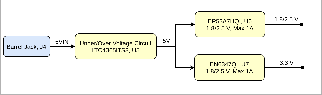
Power and Power-On Sequence
...
Power supply with minimum current capability of xx 2 A for system startup is recommended.
...
| Scroll Title |
|---|
| anchor | Table_PWR_PC |
|---|
| title | Power Consumption |
|---|
|
| Scroll Table Layout |
|---|
| orientation | portrait |
|---|
| sortDirection | ASC |
|---|
| repeatTableHeaders | default |
|---|
| style | |
|---|
| widths | |
|---|
| sortByColumn | 1 |
|---|
| sortEnabled | false |
|---|
| cellHighlighting | true |
|---|
|
| Power Input Pin | Typical Current |
|---|
| VIN5VIN | TBD* |
|
* TBD - To Be Determined
...
| Scroll Title |
|---|
| anchor | Figure_PWR_PD |
|---|
| title | Power Distribution |
|---|
|
| Scroll Ignore |
|---|
| draw.io Diagram |
|---|
| border | false |
|---|
| |
|---|
| diagramName | TEMB0005_PWR_PD |
|---|
| simpleViewer | false |
|---|
| width | 639 |
|---|
| links | auto |
|---|
| tbstyle | hidden |
|---|
| diagramDisplayName | |
|---|
| lbox | true |
|---|
| diagramWidth | 641 |
|---|
| revision | 12 |
|---|
|
|
| Scroll Only |
|---|
|
|
Power-On Sequence
| Scroll Title |
|---|
| anchor | Figure_PWR_PS |
|---|
| title | Power Sequency |
|---|
|
| Scroll Ignore |
|---|
| draw.io Diagram |
|---|
| border | false |
|---|
| |
|---|
| diagramName | TEMB0005_PWR_PS |
|---|
| simpleViewer | false |
|---|
| width | 639 |
|---|
| links | auto |
|---|
| tbstyle | hidden |
|---|
| diagramDisplayName | |
|---|
| lbox | true |
|---|
| diagramWidth | 641 |
|---|
| revision | 1 |
|---|
|
|
| Scroll Only |
|---|
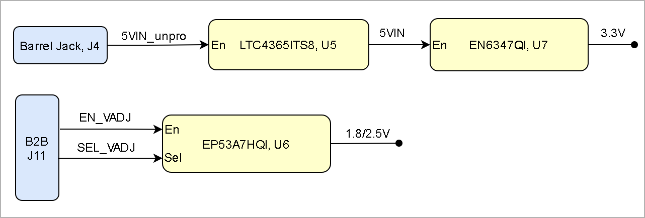 Image Removed Image Removed
|
|
Voltage Monitor Circuit
| Scroll Only |
|---|
Image Added |
|
| Scroll Title |
|---|
| anchor | Figure_PWR_VMC |
|---|
| title | Voltage Monitor Circuit |
|---|
|
| Scroll Ignore |
|---|
Create DrawIO object here: Attention if you copy from other page, objects are only linked. |
| Scroll Only |
|---|
image link to the generate DrawIO PNG file of this page. This is a workaround until scroll pdf export bug is fixed |
|
Power Rails
| Scroll Title |
|---|
| anchor | Table_PWR_PR |
|---|
| title | Module power rails. |
|---|
|
| Scroll Table Layout |
|---|
| orientation | portrait |
|---|
| sortDirection | ASC |
|---|
| repeatTableHeaders | default |
|---|
| style | |
|---|
| widths | |
|---|
| sortByColumn | 1 |
|---|
| sortEnabled | false |
|---|
| cellHighlighting | true |
|---|
|
| Power Rail Name | B2B Connector J11 Pin |
|---|
JM1 | CRUVI Connector J5 Pin | B2B Connector J6 Pin |
|---|
JM2 B2B Connector J7 Pin | B2B Connector |
|---|
JM3 |
Bank Voltages
| 3.3V | 1, 2, 3, 4 | - | 10 | 10 | 10 | Output |
| | VDAJ | 22 | 36 | - | - | - | Output |
| | 5VIN | - | - | 12 | 12 | 12 | Output |
|
| Scroll Title |
|---|
| anchor | Table_PWR_BV |
|---|
| title | Zynq SoC bank voltages. |
|---|
|
| Scroll Table Layout |
|---|
|
| orientation | portrait |
|---|
| sortDirection | ASC |
|---|
| repeatTableHeaders | default |
|---|
style | widths | | sortByColumn | 1 |
|---|
| sortEnabled | false |
|---|
| cellHighlighting | true |
|---|
Board to Board Connectors
| Page properties |
|---|
|
- This section is optional and only for modules.
use "include page" macro and link to the general B2B connector page of the module series, For example: 6 x 6 SoM LSHM B2B Connectors
| Include Page |
|---|
| PD:6 x 6 SoM LSHM B2B ConnectorsPD: |
|---|
| 6 x 6 SoM LSHM B2B Connectors |
|---|
|
|
? x ? modules use two or three Samtec Micro Tiger Eye Connector on the bottom side.
3 x REF-??????? (compatible to ????????), (?? pins, ?? per row)
| Include Page |
|---|
| DRAFT:3.1 x 5.6 SoM ST5/SS5 B2B Connectors |
|---|
| DRAFT:3.1 x 5.6 SoM ST5/SS5 B2B Connectors |
|---|
|
CRUVI B2B Connectors
| Include Page |
|---|
| CRUVI B2B Connectors |
|---|
| CRUVI B2B Connectors |
|---|
|
...
Technical Specifications
Absolute Maximum Ratings
| Scroll Title |
|---|
| anchor | Table_TS_AMR |
|---|
| title | PS absolute maximum ratings |
|---|
|
| Scroll Table Layout |
|---|
| orientation | portrait |
|---|
| sortDirection | ASC |
|---|
| repeatTableHeaders | default |
|---|
| style | |
|---|
| widths | |
|---|
| sortByColumn | 1 |
|---|
| sortEnabled | false |
|---|
| cellHighlighting | true |
|---|
|
| Symbols | Description | Min | Max | Unit |
|---|
| VIN | Input Supply Voltage | 2.5 | 34 | V | V | V | V | V | V | V | V | T_STG | Storage Temperature | -55 | 125 | °C |
|
Recommended Operating Conditions
...
| Scroll Title |
|---|
| anchor | Table_TS_ROC |
|---|
| title | Recommended operating conditions. |
|---|
|
| Scroll Table Layout |
|---|
| orientation | portrait |
|---|
| sortDirection | ASC |
|---|
| repeatTableHeaders | default |
|---|
| style | |
|---|
| widths | |
|---|
| sortByColumn | 1 |
|---|
| sortEnabled | false |
|---|
| cellHighlighting | true |
|---|
|
| Parameter | Min | Max | Units | Reference Document |
|---|
| VIN | 4.06 | 5.58 | V | See the carrier datasheets. | | T_OPT | 0 | 70 | °C | Push button | V | See ???? datasheets. | V | See Xilinx ???? datasheet. | V | See Xilinx ???? datasheet. | V | See Xilinx ???? datasheet. | V | See Xilinx ???? datasheet. | V | See Xilinx ???? datasheet. | V | See Xilinx ???? datasheet. | °C | See Xilinx ???? datasheet. | °C | See Xilinx ???? datasheet. |
|
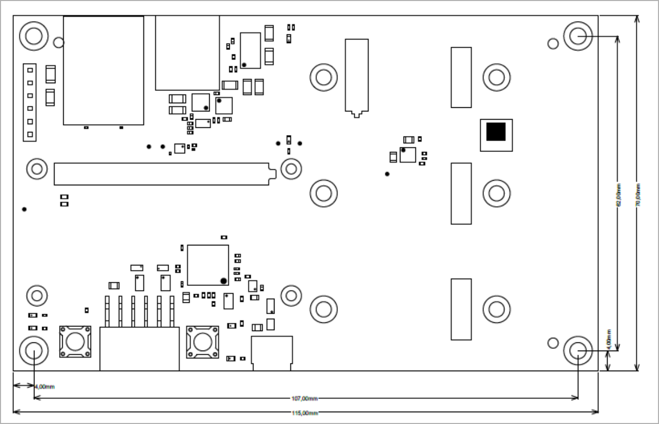
Physical Dimensions
Module size: ?? 115 mm × ?? 70 mm. Please download the assembly diagram for exact numbers.
Mating height with standard connectors: ? 4 mm.
PCB thickness: ?? 1.6 mm.
| Page properties |
|---|
|
In 'Physical Dimension' section, top and bottom view of module must be inserted, information regarding physical dimensions can be obtained through webpage for product in Shop.Trenz, (Download> Documents> Assembly part) for every SoM. For Example: for Module TE0728, Physical Dimension information can be captured by snipping tools from the link below: https://www.trenz-electronic.de/fileadmin/docs/Trenz_Electronic/Modules_and_Module_Carriers/5.2x7.6/TE0745/REV02/Documents/AD-TE0745-02-30-1I.PDF
|
...
| Scroll Title |
|---|
| anchor | Figure_TS_PD |
|---|
| title | Physical Dimension |
|---|
|
| Scroll Ignore |
|---|
| draw.io Diagram |
|---|
| border | false |
|---|
| |
|---|
| diagramName | TEMB0005_TS_PD |
|---|
| simpleViewer | false |
|---|
| width | 639 |
|---|
| links | auto |
|---|
| tbstyle | hidden |
|---|
| diagramDisplayName | |
|---|
| lbox | true |
|---|
| diagramWidth | 641 |
|---|
| revision | 12 |
|---|
|
|
| Scroll Only |
|---|
| scroll-pdf | true |
|---|
| scroll-office | true |
|---|
| scroll-chm | true |
|---|
| scroll-docbook | true |
|---|
| scroll-eclipsehelp | true |
|---|
| scroll-epub | true |
|---|
| scroll-html | true |
|---|
| 
|
|
...
| Scroll Title |
|---|
| anchor | Table_VCP_SO |
|---|
| title | Trenz Electronic Shop Overview |
|---|
|
| Scroll Table Layout |
|---|
| orientation | portrait |
|---|
| sortDirection | ASC |
|---|
| repeatTableHeaders | default |
|---|
| style | |
|---|
| widths | |
|---|
| sortByColumn | 1 |
|---|
| sortEnabled | false |
|---|
| cellHighlighting | true |
|---|
|
|
Revision History
Hardware Revision History
...
| Scroll Title |
|---|
| anchor | Table_RH_HRH |
|---|
| title | Hardware Revision History |
|---|
|
| Scroll Table Layout |
|---|
| orientation | portrait |
|---|
| sortDirection | ASC |
|---|
| repeatTableHeaders | default |
|---|
| style | |
|---|
| widths | |
|---|
| sortByColumn | 1 |
|---|
| sortEnabled | false |
|---|
| cellHighlighting | true |
|---|
|
| Date | Revision | Changes | Documentation Link |
|---|
| 2020-05-20 | REV01 | Initial Release | --- |
|
Hardware revision number can be found on the PCB board together with the module model number separated by the dash.
| Scroll Title |
|---|
| anchor | Figure_RV_HRN |
|---|
| title | Board hardware revision number. |
|---|
|
| Scroll Ignore |
|---|
| draw.io Diagram |
|---|
| border | false |
|---|
| |
|---|
| diagramName | TEMB0005_RV_HRN |
|---|
| simpleViewer | false |
|---|
| width | 200 |
|---|
| links | auto |
|---|
| tbstyle | hidden |
|---|
| diagramDisplayName | |
|---|
| lbox | true |
|---|
| diagramWidth | 641167 |
|---|
| revision | 14 |
|---|
|
|
| Scroll Only |
|---|
 Image Removed Image Removed Image Added Image Added
|
|
Document Change History
...
| Scroll Title |
|---|
| anchor | Table_RH_DCH |
|---|
| title | Document change history. |
|---|
|
| Scroll Table Layout |
|---|
| orientation | portrait |
|---|
| sortDirection | ASC |
|---|
| repeatTableHeaders | default |
|---|
| style | |
|---|
| widths | |
|---|
| sortByColumn | 1 |
|---|
| sortEnabled | false |
|---|
| cellHighlighting | true |
|---|
|
| Date | Revision | Contributor | Description |
|---|
| Page info |
|---|
| infoType | Modified date |
|---|
| dateFormat | yyyy-MM-dd |
|---|
| type | Flat |
|---|
|
| | Page info |
|---|
| infoType | Current version |
|---|
| prefix | v. |
|---|
| type | Flat |
|---|
| showVersions | false |
|---|
|
| | Page info |
|---|
| infoType | Modified by |
|---|
| type | Flat |
|---|
| showVersions | false |
|---|
|
| | -- | all | | Page info |
|---|
| infoType | Modified users |
|---|
| type | Flat |
|---|
| showVersions | false |
|---|
|
| |
|
...