...
| Scroll Title |
|---|
| anchor | Figure_OV_BD |
|---|
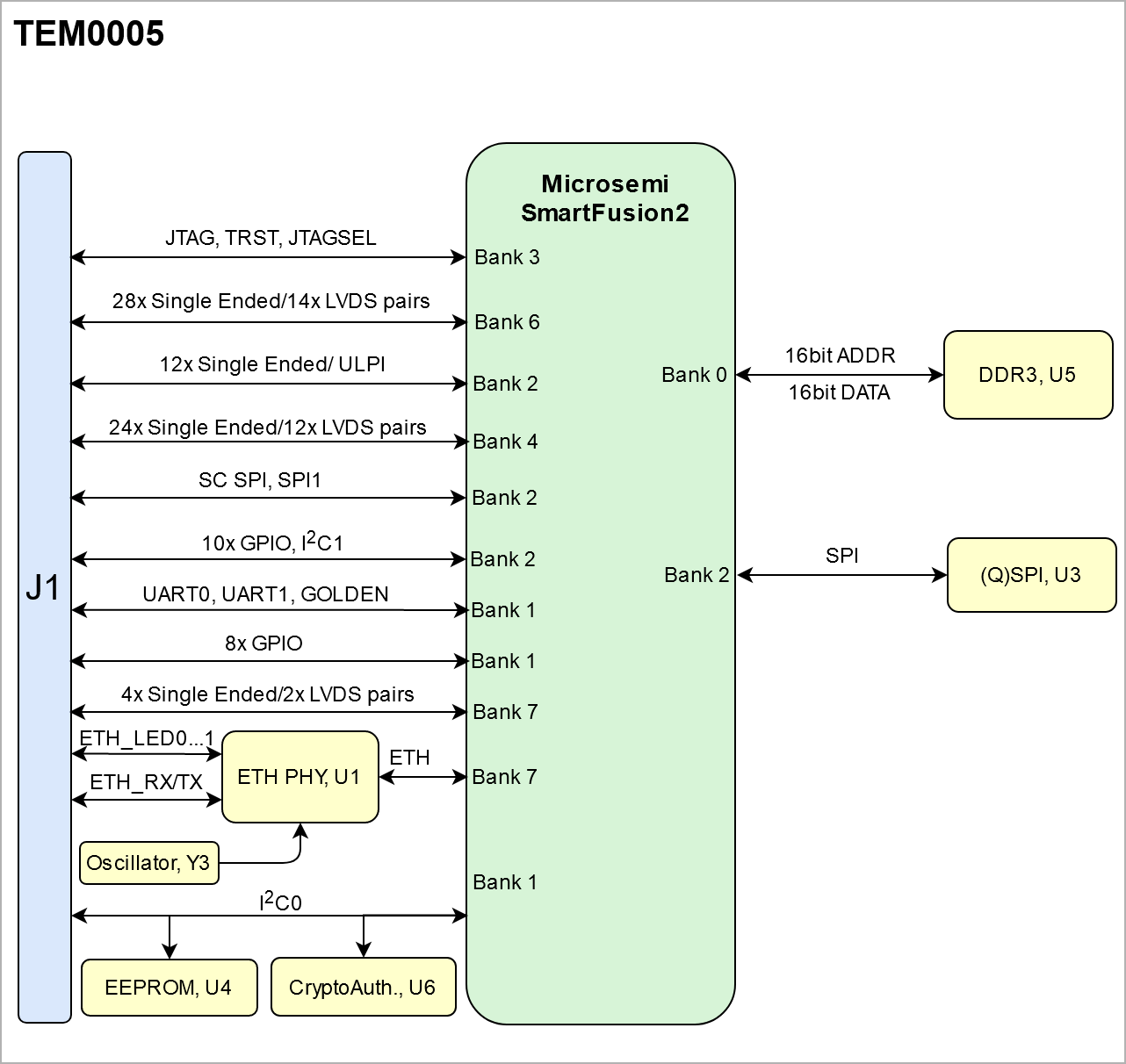
| title | TEM0005 block diagram |
|---|
|
| Scroll Ignore |
|---|
| scroll-pdf | true |
|---|
| scroll-office | true |
|---|
| scroll-chm | true |
|---|
| scroll-docbook | true |
|---|
| scroll-eclipsehelp | true |
|---|
| scroll-epub | true |
|---|
| scroll-html | true |
|---|
| | draw.io Diagram |
|---|
| border | false |
|---|
| |
|---|
| diagramName | TEM0005_OV_BD |
|---|
| simpleViewer | false |
|---|
| width | 639 |
|---|
| links | auto |
|---|
| tbstyle | hidden |
|---|
| diagramDisplayName | |
|---|
| lbox | true |
|---|
| diagramWidth | 641 |
|---|
| revision | 9 |
|---|
|
%3CmxGraphModel%3E%3Croot%3E%3CmxCell%20id%3D%220%22%2F%3E%3CmxCell%20id%3D%221%22%20parent%3D%220%22%2F%3E%3CmxCell%20id%3D%222%22%20value%3D%22%22%20style%3D%22rounded%3D1%3BwhiteSpace%3Dwrap%3Bhtml%3D1%3BfillColor%3D%23D7F4D7%3B%22%20vertex%3D%221%22%20parent%3D%221%22%3E%3CmxGeometry%20x%3D%22293%22%20y%3D%2288%22%20width%3D%22153%22%20height%3D%22461%22%20as%3D%22geometry%22%2F%3E%3C%2FmxCell%3E%3CmxCell%20id%3D%223%22%20value%3D%22Bank%204%22%20style%3D%22text%3Bhtml%3D1%3BstrokeColor%3Dnone%3BfillColor%3Dnone%3Balign%3Dcenter%3BverticalAlign%3Dmiddle%3BwhiteSpace%3Dwrap%3Brounded%3D0%3B%22%20vertex%3D%221%22%20parent%3D%221%22%3E%3CmxGeometry%20x%3D%22279%22%20y%3D%22233%22%20width%3D%2248%22%20height%3D%2220%22%20as%3D%22geometry%22%2F%3E%3C%2FmxCell%3E%3CmxCell%20id%3D%224%22%20value%3D%22%26lt%3Bdiv%20align%3D%26quot%3Bcenter%26quot%3B%20style%3D%26quot%3Bfont-size%3A%2014px%26quot%3B%26gt%3B%26lt%3Bb%26gt%3BMicrosemi%26lt%3B%2Fb%26gt%3B%26lt%3B%2Fdiv%26gt%3B%26lt%3Bdiv%20align%3D%26quot%3Bcenter%26quot%3B%20style%3D%26quot%3Bfont-size%3A%2014px%26quot%3B%26gt%3B%26lt%3Bb%26gt%3BSmart%20Fusion2%26lt%3B%2Fb%26gt%3B%26lt%3B%2Fdiv%26gt%3B%22%20style%3D%22text%3Bhtml%3D1%3Balign%3Dcenter%3B%22%20vertex%3D%221%22%20parent%3D%221%22%3E%3CmxGeometry%20x%3D%22318%22%20y%3D%22105%22%20width%3D%22100%22%20height%3D%2250%22%20as%3D%22geometry%22%2F%3E%3C%2FmxCell%3E%3CmxCell%20id%3D%225%22%20value%3D%22Bank%208%22%20style%3D%22text%3Bhtml%3D1%3BstrokeColor%3Dnone%3BfillColor%3Dnone%3Balign%3Dcenter%3BverticalAlign%3Dmiddle%3BwhiteSpace%3Dwrap%3Brounded%3D0%3B%22%20vertex%3D%221%22%20parent%3D%221%22%3E%3CmxGeometry%20x%3D%22310%22%20y%3D%22267%22%20width%3D%2244%22%20height%3D%2220%22%20as%3D%22geometry%22%2F%3E%3C%2FmxCell%3E%3CmxCell%20id%3D%226%22%20value%3D%22Bank%203%22%20style%3D%22text%3Bhtml%3D1%3BstrokeColor%3Dnone%3BfillColor%3Dnone%3Balign%3Dcenter%3BverticalAlign%3Dmiddle%3BwhiteSpace%3Dwrap%3Brounded%3D0%3B%22%20vertex%3D%221%22%20parent%3D%221%22%3E%3CmxGeometry%20x%3D%22306%22%20y%3D%22369%22%20width%3D%2245%22%20height%3D%2220%22%20as%3D%22geometry%22%2F%3E%3C%2FmxCell%3E%3CmxCell%20id%3D%227%22%20value%3D%22Bank%205%22%20style%3D%22text%3Bhtml%3D1%3BstrokeColor%3Dnone%3BfillColor%3Dnone%3Balign%3Dcenter%3BverticalAlign%3Dmiddle%3BwhiteSpace%3Dwrap%3Brounded%3D0%3B%22%20vertex%3D%221%22%20parent%3D%221%22%3E%3CmxGeometry%20x%3D%22319%22%20y%3D%22413%22%20width%3D%2243%22%20height%3D%2220%22%20as%3D%22geometry%22%2F%3E%3C%2FmxCell%3E%3CmxCell%20id%3D%228%22%20value%3D%22Bank%206%22%20style%3D%22text%3Bhtml%3D1%3BstrokeColor%3Dnone%3BfillColor%3Dnone%3Balign%3Dcenter%3BverticalAlign%3Dmiddle%3BwhiteSpace%3Dwrap%3Brounded%3D0%3B%22%20vertex%3D%221%22%20parent%3D%221%22%3E%3CmxGeometry%20x%3D%22263%22%20y%3D%22397%22%20width%3D%2249%22%20height%3D%2220%22%20as%3D%22geometry%22%2F%3E%3C%2FmxCell%3E%3CmxCell%20id%3D%229%22%20value%3D%22Bank%202%22%20style%3D%22text%3Bhtml%3D1%3BstrokeColor%3Dnone%3BfillColor%3Dnone%3Balign%3Dcenter%3BverticalAlign%3Dmiddle%3BwhiteSpace%3Dwrap%3Brounded%3D0%3B%22%20vertex%3D%221%22%20parent%3D%221%22%3E%3CmxGeometry%20x%3D%22293%22%20y%3D%22298%22%20width%3D%2247%22%20height%3D%2220%22%20as%3D%22geometry%22%2F%3E%3C%2FmxCell%3E%3CmxCell%20id%3D%2210%22%20value%3D%22Bank%207%22%20style%3D%22text%3Bhtml%3D1%3BstrokeColor%3Dnone%3BfillColor%3Dnone%3Balign%3Dcenter%3BverticalAlign%3Dmiddle%3BwhiteSpace%3Dwrap%3Brounded%3D0%3B%22%20vertex%3D%221%22%20parent%3D%221%22%3E%3CmxGeometry%20x%3D%22290%22%20y%3D%22336%22%20width%3D%2244%22%20height%3D%2220%22%20as%3D%22geometry%22%2F%3E%3C%2FmxCell%3E%3C%2Froot%3E%3C%2FmxGraphModel%3E
|
| Scroll Only |
|---|
|
|
Main Components
...
| Scroll Title |
|---|
| anchor | Figure_OV_MC |
|---|
| title | TEM0005 main components |
|---|
|
| Scroll Ignore |
|---|
| draw.io Diagram |
|---|
| border | false |
|---|
| |
|---|
| diagramName | TEM0005_OV_MC |
|---|
| simpleViewer | false |
|---|
| width | 600 |
|---|
| links | auto |
|---|
| tbstyle | hidden |
|---|
| diagramDisplayName | |
|---|
| lbox | true |
|---|
| diagramWidth | 641 |
|---|
| revision | 720 |
|---|
|
|
| Scroll Only |
|---|
|
|
- Microsemi SmartFusion, U2
- Reg, U7
- EEPROM, U4
- 10/100 Mb Ethernet, U1
- QSPI Flash, U3
- Authentication IC, U6
- DDR3 Memory, U5
- B2B Connector, J1
- ...
- ...
- ...
Initial Delivery State
| Page properties |
|---|
|
Notes : Only components like EEPROM, QSPI flash can be initialized by default at manufacture. If there is no components which might have initial data ( possible on carrier) you must keep the table empty |
...
| Scroll Title |
|---|
| anchor | Table_OV_IDS |
|---|
| title | Initial delivery state of programmable devices on the module |
|---|
|
| Scroll Table Layout |
|---|
| orientation | portrait |
|---|
| sortDirection | ASC |
|---|
| repeatTableHeaders | default |
|---|
| style | |
|---|
| widths | |
|---|
| sortByColumn | 1 |
|---|
| sortEnabled | false |
|---|
| cellHighlighting | true |
|---|
|
Storage device name | Content | Notes |
|---|
Quad SPI Flash | Not Programmed |
| | EEPROM | Not Programmed |
| | DDR3 SDRAM | Not ProgrammedSystem Controller CPLD |
|
|
Configuration Signals
| Page properties |
|---|
|
- Overview of Boot Mode, Reset, Enables.
|
| Scroll Title |
|---|
|
| anchor | Table_OV_BP |
|---|
title | Boot process | | Scroll Table Layout |
|---|
| | orientation | portrait |
|---|
| sortDirection | ASC |
|---|
| repeatTableHeaders | default |
|---|
style | widths | | sortByColumn | 1 |
|---|
| sortEnabled | false |
|---|
| cellHighlighting | true |
|---|
MODE Signal State | Boot Mode
| Scroll Title |
|---|
| anchor | Table_OV_RST |
|---|
| title | Reset process. |
|---|
|
| Scroll Table Layout |
|---|
| orientation | portrait |
|---|
| sortDirection | ASC |
|---|
| repeatTableHeaders | default |
|---|
| style | |
|---|
| widths | |
|---|
| sortByColumn | 1 |
|---|
| sortEnabled | false |
|---|
| cellHighlighting | true |
|---|
|
Signal | B2B | I/O | Note |
|---|
RESET
| J1-11 |
| Active low reset |
|
Signals, Interfaces and Pins
...
JTAG Interface
JTAG access to the TExxxx TEM0005 SoM through B2B connector JMXJ1.
| Scroll Title |
|---|
| anchor | Table_SIP_JTG |
|---|
| title | JTAG pins connection |
|---|
|
| Scroll Table Layout |
|---|
| orientation | portrait |
|---|
| sortDirection | ASC |
|---|
| repeatTableHeaders | default |
|---|
| style | |
|---|
| widths | |
|---|
| sortByColumn | 1 |
|---|
| sortEnabled | false |
|---|
| cellHighlighting | true |
|---|
|
JTAG Signal | B2B Connector |
|---|
| TMS | J1-14 | | TDI | J1-8 | | TDO | J1-10 | | TCK | J1-12 | | JTAG_EN |
|
...
Test Points
| Page properties |
|---|
|
you must fill the table below with group of MIOs Test Point which are connected to a specific components or peripherals, you do not have to specify pins in B2B, Just mention which B2B is connected to MIOs. The rest is clear in the Schematicindicated as TP in a schematic. If there is no Test Point remarked in the schematic, delet the Test Point section. Example: | Test Point | Signal | MIO Pin | Connected to | B2B | Notes |
|---|
| MIO12...14 | SPI_CS , SPI_DQ0... SPI_DQ3 SPI_SCK | J2 | QSPI | | 10 | PWR_PL_OK | J2-120 |
|
|
| Scroll Title |
|---|
| anchor | Table_SIP_MIOsTPs |
|---|
| title | MIOs pinsTest Points Information |
|---|
|
| Scroll Table Layout |
|---|
| orientation | portrait |
|---|
| sortDirection | ASC |
|---|
| repeatTableHeaders | default |
|---|
| style | |
|---|
| widths | |
|---|
| sortByColumn | 1 |
|---|
| sortEnabled | false |
|---|
| cellHighlighting | true |
|---|
|
|
Test Points
On-board Peripherals
| Page properties |
|---|
| you must fill the table below with group of Test Point which are indicated as TP in a schematic. If there is no Test Point remarked in the schematic, delet the Test Point section.
Example:
| Test Point | Signal | B2B | Notes |
|---|
10 | PWR_PL_OK | J2-120 | | Notes : - add subsection for every component which is important for design, for example:
- Two 100 Mbit Ethernet Transciever PHY
- USB PHY
- Programmable Clock Generator
- Oscillators
- eMMCs
- RTC
- FTDI
- ...
- DIP-Switches
- Buttons
- LEDs
|
| Page properties |
|---|
|
Notes : In the on-board peripheral table "chip/Interface" must be linked to the corresponding chapter or subsection |
| Scroll Title |
|---|
| anchor | Table_OBP |
|---|
| title | On board peripherals |
|---|
|
| Scroll Title |
|---|
| anchor | Table_SIP_TPs |
|---|
| title | Test Points Information |
|---|
|
| Scroll Table Layout |
|---|
| orientation | portrait |
|---|
| sortDirection | ASC |
|---|
| repeatTableHeaders | default |
|---|
| style | |
|---|
| widths | |
|---|
| sortByColumn | 1 |
|---|
| sortEnabled | false |
|---|
| cellHighlighting | true |
|---|
|
|
| Test Point | Signal | Connected to | Notes |
|---|
...
| Chip/Interface | Designator | Notes |
|---|
| QSPI | U3 |
| | DDR3 SDRAM | U5 |
| | EEPROM | U4 |
| | Authentication IC | U6 |
| | Ethernet | U1 |
|
|
Quad SPI Flash Memory
| Page properties |
|---|
|
Notes : - add subsection for every component which is important for design, for example:
- Two 100 Mbit Ethernet Transciever PHY
- USB PHY
- Programmable Clock Generator
- Oscillators
- eMMCs
- RTC
- FTDI
- ...
- DIP-Switches
- Buttons
- LEDs
|
| Page properties |
|---|
|
Notes : In the on-board peripheral table "chip/Interface" must be linked to the corresponding chapter or subsectionMinimum and Maximum density of quad SPI flash must be mentioned for other assembly options. |
| Scroll Title |
|---|
| anchor | Table_OBP_SPI |
|---|
| title | On board peripheralsQuad SPI interface MIOs and pins |
|---|
|
| Scroll Table Layout |
|---|
| orientation | portrait |
|---|
| sortDirection | ASC |
|---|
| repeatTableHeaders | default |
|---|
| style | |
|---|
| widths | |
|---|
| sortByColumn | 1 |
|---|
| sortEnabled | false |
|---|
| cellHighlighting | true |
|---|
|
|
| Chip/Interface | Designator | Notes |
|---|
Quad SPI Flash Memory
...
Notes :
...
| MIO Pin | Schematic | U?? Pin | Notes |
|---|
|
|
|
|
|
|
|
|
|
|
|
|
|
|
|
|
|
|
|
|
|
|
|
|
|
EEPROM
| Scroll Title |
|---|
| anchor | Table_OBP_SPIEEP |
|---|
| title | Quad SPI I2C EEPROM interface MIOs and pins |
|---|
|
| Scroll Table Layout |
|---|
| orientation | portrait |
|---|
| sortDirection | ASC |
|---|
| repeatTableHeaders | default |
|---|
| style | |
|---|
| widths | |
|---|
| sortByColumn | 1 |
|---|
| sortEnabled | false |
|---|
| cellHighlighting | true |
|---|
|
| MIO Pin | Schematic | U?? Pin | Notes |
|---|
|
...
| Scroll Title |
|---|
| anchor | Table_OBP_RTCI2C_EEPROM |
|---|
| title | I2C interface MIOs and pinsaddress for EEPROM |
|---|
|
anchor| Scroll Table Layout |
|---|
| orientation | portrait |
|---|
| sortDirection | ASC |
|---|
| repeatTableHeaders | default |
|---|
| style | |
|---|
| widths | |
|---|
| sortByColumn | 1 |
|---|
| sortEnabled | false |
|---|
| cellHighlighting | true |
|---|
|
|
| Scroll Title |
|---|
| Table_OBP_ | _RTCtitle | I2C | for RTCscroll-tablelayoutorientationportrait
|
|---|
DDR3 SDRAM
sortDirection| Page properties |
|---|
ASC | repeatTableHeaders | default | style | widths |
| sortByColumn | 1 |
|---|
| sortEnabled | false |
|---|
| cellHighlighting | true |
|---|
| MIO Pin | I2C Address | Designator | Notes |
|---|
...
| anchor | Table_OBP_EEP |
|---|
| title | I2C EEPROM interface MIOs and pins |
|---|
...
| anchor | Table_OBP_I2C_EEPROM |
|---|
| title | I2C address for EEPROM |
|---|
...
LEDs
...
| anchor | Table_OBP_LED |
|---|
| title | On-board LEDs |
|---|
...
DDR3 SDRAM
| Page properties |
|---|
|
Notes : Minimum and Maximum density of DDR3 SDRAM must be mentioned for other assembly options. (pay attention to supported address length for DDR3) |
The TE???? SoM has ??? GByte volatile DDR3 SDRAM IC for storing user application code and data.
- Part number:
- Supply voltage:
- Speed:
- NOR Flash
- Temperature:
Ethernet
...
| anchor | Table_OBP_ETH |
|---|
| title | Ethernet PHY to Zynq SoC connections |
|---|
...
CAN Transceiver
...
| anchor | Table_OBP_CAN |
|---|
| title | CAN Tranciever interface MIOs |
|---|
...
| anchor | Table_OBP_CLK |
|---|
| title | Osillators |
|---|
...
Programmable Clock Generator
...
Notes : Minimum and Maximum density of DDR3 SDRAM must be mentioned for other assembly options. (pay attention to supported address length for DDR3) |
The TE???? SoM has ??? GByte volatile DDR3 SDRAM IC for storing user application code and data.
- Part number:
- Supply voltage:
- Speed:
- NOR Flash
- Temperature:
Ethernet
| Scroll Title |
|---|
| anchor | Table_OBP_PCLKETH |
|---|
| title | Programmable Clock Generator Inputs and OutputsEthernet PHY to Zynq SoC connections |
|---|
|
| Scroll Table Layout |
|---|
| orientation | portrait |
|---|
| sortDirection | ASC |
|---|
| repeatTableHeaders | default |
|---|
| style | |
|---|
| widths | |
|---|
| sortByColumn | 1 |
|---|
| sortEnabled | false |
|---|
| cellHighlighting | true |
|---|
|
Pin| Pin | Signal Name | Connected to |
|---|
Direction | Note | IN0 | IN1 | IN2 | IN3 | XAXB | SCLK | SDA | OUT0 | OUT1 | OUT2 | OUT3 | OUT4 | OUT5 | OUT6 | OUT7 |
|
Clock Sources
| Scroll Title |
|---|
| anchor | Table_OBP_CLK |
|---|
| title | Osillators |
|---|
|
| Scroll Table Layout |
|---|
| orientation | portrait |
|---|
| sortDirection | ASC |
|---|
| repeatTableHeaders | default |
|---|
| style | |
|---|
| widths | |
|---|
| sortByColumn | 1 |
|---|
| sortEnabled | false |
|---|
| cellHighlighting | true |
|---|
|
| Designator | Description | Frequency | Note |
|---|
| Y3 | Crystal Oscillator | 25 MHz |
OUT8/OUT9
|
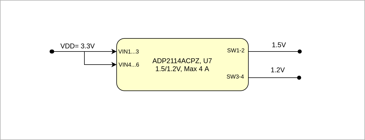
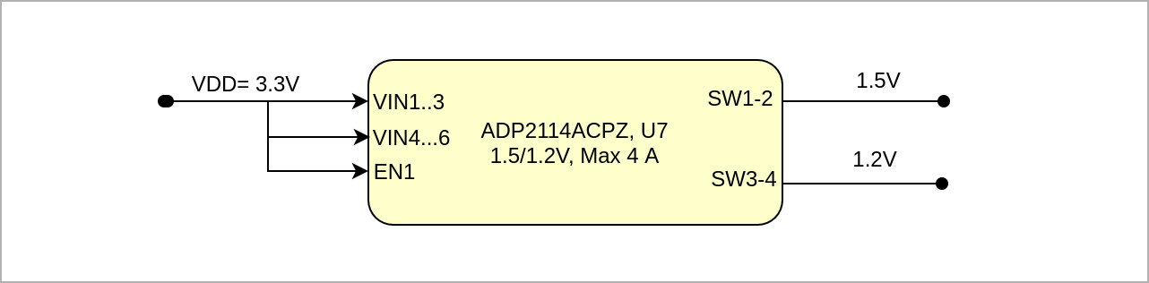
Power and Power-On Sequence
...
Power supply with minimum current capability of xx 1.5 A for system startup is recommended.
...
| Scroll Title |
|---|
| anchor | Figure_PWR_PD |
|---|
| title | Power Distribution |
|---|
|
| Scroll Ignore |
|---|
| draw.io Diagram |
|---|
| border | false |
|---|
| |
|---|
| diagramName | TEM0005_PWR_PD |
|---|
| simpleViewer | false |
|---|
| width | 639 |
|---|
| links | auto |
|---|
| tbstyle | hidden |
|---|
| diagramDisplayName | |
|---|
| lbox | true |
|---|
| diagramWidth | 641 |
|---|
| revision | 3 |
|---|
|
|
| Scroll Only |
|---|
|
|
...
| Scroll Title |
|---|
| anchor | Figure_PWR_PS |
|---|
| title | Power Sequency |
|---|
|
| Scroll Ignore |
|---|
| draw.io Diagram |
|---|
| border | false |
|---|
| |
|---|
| diagramName | TEM0005_PWR_PS |
|---|
| simpleViewer | false |
|---|
| width | 639 |
|---|
| links | auto |
|---|
| tbstyle | hidden |
|---|
| diagramDisplayName | |
|---|
| lbox | true |
|---|
| diagramWidth | 641 |
|---|
| revision | 1 |
|---|
|
|
| Scroll Only |
|---|
|
|
...
| Scroll Title |
|---|
| anchor | Table_PWR_PR |
|---|
| title | Module power rails. |
|---|
|
| Scroll Table Layout |
|---|
| orientation | portrait |
|---|
| sortDirection | ASC |
|---|
| repeatTableHeaders | default |
|---|
| style | |
|---|
| widths | |
|---|
| sortByColumn | 1 |
|---|
| sortEnabled | false |
|---|
| cellHighlighting | true |
|---|
|
| Power Rail Name | B2B Connector |
|---|
B2B Connector JM2 Pin | B2B Connector JM3 Pin | Direction | Notes| Direction | Notes |
|---|
| 3.3V | 1, 2, 3, 4 | Output |
| | VDDI6 | 22 | Input |
|
|
Bank Voltages
| Scroll Title |
|---|
| anchor | Table_PWR_BV |
|---|
| title | Zynq SoC bank voltages. |
|---|
|
| Scroll Table Layout |
|---|
| orientation | portrait |
|---|
| sortDirection | ASC |
|---|
| repeatTableHeaders | default | style | widths |
|---|
| sortByColumn | 1 |
|---|
| sortEnabled | false |
|---|
| cellHighlighting | true |
|---|
| | style | |
|---|
| widths | |
|---|
| sortByColumn | 1 |
|---|
| sortEnabled | false |
|---|
| cellHighlighting | true |
|---|
|
| Schematic Name | | Notes |
|---|
| Bank0 | VDDI0 | 1.5V |
| | Bank1 | VDDI1 | 3.3V |
| | Bank2 | VDDI2 | 3.3V |
| | Bank3 | VDDI3 | 3.3V |
| | Bank4 | VDDI4 | 3.3V |
| | Bank5 | VDDI6 | ? |
| | Bank6 | VDDI6 | ? |
| | Bank7 | VDDI7 | 3.3V | | Schematic Name | | Notes |
|
|
Board to Board Connectors
...
| Scroll Title |
|---|
| anchor | Table_TS_AMR |
|---|
| title | PS absolute maximum ratings |
|---|
|
| Scroll Table Layout |
|---|
| orientation | portrait |
|---|
| sortDirection | ASC |
|---|
| repeatTableHeaders | default |
|---|
| style | |
|---|
| widths | |
|---|
| sortByColumn | 1 |
|---|
| sortEnabled | false |
|---|
| cellHighlighting | true |
|---|
|
| Symbols | Description | Min | Max | Unit |
|---|
| VVINV | Input Supply Voltage |
|
| V | V | V | V | V | V | | STG_T | Storage Temperature |
|
| °C |
|
Recommended Operating Conditions
...
| Scroll Title |
|---|
| anchor | Table_TS_ROC |
|---|
| title | Recommended operating conditions. |
|---|
|
| Scroll Table Layout |
|---|
| orientation | portrait |
|---|
| sortDirection | ASC |
|---|
| repeatTableHeaders | default |
|---|
| style | |
|---|
| widths | |
|---|
| sortByColumn | 1 |
|---|
| sortEnabled | false |
|---|
| cellHighlighting | true |
|---|
|
| Parameter | Min | Max | Units | Reference Document | | Max | Units | Reference Document |
|---|
| VIN | V | See ???? datasheets. | V | See Xilinx ???? datasheet. | V | See Xilinx ???? datasheet. | V | See Xilinx ???? datasheet. | V | See Xilinx ???? datasheet. | V | See Xilinx ???? datasheet. |
|
| V | See Xilinx ???? datasheetdatasheets. | | °C | See Xilinx ???? datasheet.OPT_T |
|
| °C | See Xilinx ???? datasheet. |
|
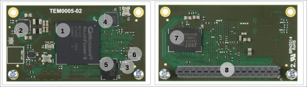
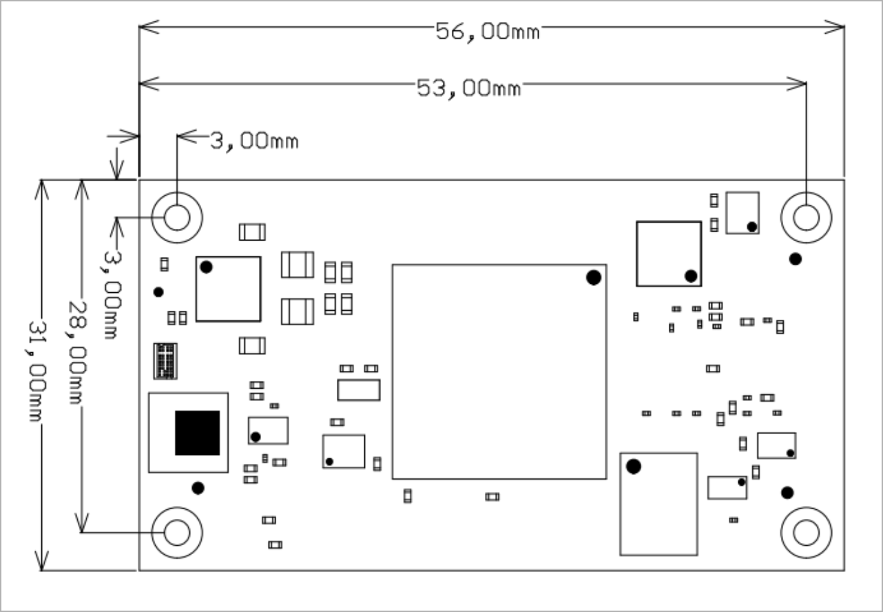
Physical Dimensions
Module size: ?? 56 mm × ?? 31 mm. Please download the assembly diagram for exact numbers.
Mating height with standard connectors: ? 4 mm.
PCB thickness: ?? 1.6 mm.
| Page properties |
|---|
|
In 'Physical Dimension' section, top and bottom view of module must be inserted, information regarding physical dimensions can be obtained through webpage for product in Shop.Trenz, (Download> Documents> Assembly part) for every SoM. For Example: for Module TE0728, Physical Dimension information can be captured by snipping tools from the link below: https://www.trenz-electronic.de/fileadmin/docs/Trenz_Electronic/Modules_and_Module_Carriers/5.2x7.6/TE0745/REV02/Documents/AD-TE0745-02-30-1I.PDF
|
...
| Scroll Title |
|---|
| anchor | Figure_TS_PD |
|---|
| title | Physical Dimension |
|---|
|
| Scroll Ignore |
|---|
| draw.io Diagram |
|---|
| border | false |
|---|
| |
|---|
| diagramName | TEM0005_TS_PD |
|---|
| simpleViewer | false |
|---|
| width | 639 |
|---|
| links | auto |
|---|
| tbstyle | hidden |
|---|
| diagramDisplayName | |
|---|
| lbox | true |
|---|
| diagramWidth | 641 |
|---|
| revision | 23 |
|---|
|
|
| Scroll Only |
|---|
| scroll-pdf | true |
|---|
| scroll-office | true |
|---|
| scroll-chm | true |
|---|
| scroll-docbook | true |
|---|
| scroll-eclipsehelp | true |
|---|
| scroll-epub | true |
|---|
| scroll-html | true |
|---|
| 
|
|
...
| Scroll Title |
|---|
| anchor | Figure_RV_HRN |
|---|
| title | Board hardware revision number. |
|---|
|
| Scroll Ignore |
|---|
| draw.io Diagram |
|---|
| border | false |
|---|
| |
|---|
| diagramName | TEM0005_RV_HRN |
|---|
| simpleViewer | false |
|---|
| width | |
|---|
| links | auto |
|---|
| tbstyle | hidden |
|---|
| diagramDisplayName | |
|---|
| lbox | true |
|---|
| diagramWidth | 641175 |
|---|
| revision | 56 |
|---|
|
|
| Scroll Only |
|---|
|
|
Document Change History
...
| Scroll Title |
|---|
| anchor | Figure_OV_BD |
|---|
| title | TEM0005 block diagram |
|---|
|
| Scroll Ignore |
|---|
| draw.io Diagram |
|---|
| border | false |
|---|
| |
|---|
| diagramName | TEM0005_OV_BD |
|---|
| simpleViewer | false |
|---|
| width | |
|---|
| links | auto |
|---|
| tbstyle | hidden |
|---|
| diagramDisplayName | |
|---|
| lbox | true |
|---|
| diagramWidth | 641 |
|---|
| revision | 59 |
|---|
|
|
| Scroll Only |
|---|
|
|
Main Components
...
| Scroll Title |
|---|
| anchor | Figure_OV_MC |
|---|
| title | TEM0005 main components |
|---|
|
| Scroll Ignore |
|---|
| draw.io Diagram |
|---|
| border | false |
|---|
| |
|---|
| diagramName | TEM0005_OV_MC |
|---|
| simpleViewer | false |
|---|
| width | |
|---|
| links | auto |
|---|
| tbstyle | hidden |
|---|
| diagramDisplayName | |
|---|
| lbox | true |
|---|
| diagramWidth | 641 |
|---|
| revision | 720 |
|---|
|
|
| Scroll Only |
|---|
|
|
- ...
- ...
- ...
Initial Delivery State
...
| Scroll Title |
|---|
| anchor | Table_SIP_JTG |
|---|
| title | JTAG pins connection |
|---|
|
| Scroll Table Layout |
|---|
| orientation | portrait |
|---|
| sortDirection | ASC |
|---|
| repeatTableHeaders | default |
|---|
| style | |
|---|
| widths | |
|---|
| sortByColumn | 1 |
|---|
| sortEnabled | false |
|---|
| cellHighlighting | true |
|---|
|
JTAG Signal | B2B Connector |
|---|
| TMS |
| | TDI |
| | TDO |
| | TCK |
| | JTAG_EN |
|
|
MIO Pins
| Page properties |
|---|
|
you must fill the table below with group of MIOs which are connected to a specific components or peripherals, you do not have to specify pins in B2B, Just mention which B2B is connected to MIOs. The rest is clear in the Schematic. Example: | MIO Pin | Connected to | B2B | Notes |
|---|
| MIO12...14 | SPI_CS , SPI_DQ0... SPI_DQ3 SPI_SCK | J2 | QSPI |
|
...
| Scroll Title |
|---|
| anchor | Table_OBP_SPI |
|---|
| title | Quad SPI interface MIOs and pins |
|---|
|
| Scroll Table Layout |
|---|
| orientation | portrait |
|---|
| sortDirection | ASC |
|---|
| repeatTableHeaders | default |
|---|
| style | |
|---|
| widths | |
|---|
| sortByColumn | 1 |
|---|
| sortEnabled | false |
|---|
| cellHighlighting | true |
|---|
|
| MIO Pin | Schematic | U?? Pin | Notes |
|---|
|
|
|
|
|
|
|
|
|
|
|
|
|
|
|
|
|
|
|
|
|
|
|
|
|
RTC
| Scroll Title |
|---|
| anchor | Table_OBP_RTC |
|---|
| title | I2C interface MIOs and pins |
|---|
|
| Scroll Table Layout |
|---|
| orientation | portrait |
|---|
| sortDirection | ASC |
|---|
| repeatTableHeaders | default |
|---|
| style | |
|---|
| widths | |
|---|
| sortByColumn | 1 |
|---|
| sortEnabled | false |
|---|
| cellHighlighting | true |
|---|
|
| MIO Pin | Schematic | U? Pin | Notes |
|---|
|
|
|
|
|
|
|
|
|
...
| Scroll Title |
|---|
| anchor | Table_OBP_I2C_EEPROM |
|---|
| title | I2C address for EEPROM |
|---|
|
| Scroll Table Layout |
|---|
| orientation | portrait |
|---|
| sortDirection | ASC |
|---|
| repeatTableHeaders | default |
|---|
| style | |
|---|
| widths | |
|---|
| sortByColumn | 1 |
|---|
| sortEnabled | false |
|---|
| cellHighlighting | true |
|---|
|
| MIO Pin | I2C Address | Designator | Notes |
|---|
|
|
|
|
|
LEDs
| Scroll Title |
|---|
| anchor | Table_OBP_LED |
|---|
| title | On-board LEDs |
|---|
|
| Scroll Table Layout |
|---|
| orientation | portrait |
|---|
| sortDirection | ASC |
|---|
| repeatTableHeaders | default |
|---|
| style | |
|---|
| widths | |
|---|
| sortByColumn | 1 |
|---|
| sortEnabled | false |
|---|
| cellHighlighting | true |
|---|
|
| Designator | Color | Connected to | Active Level | Note |
|---|
|
|
|
|
|
|
|
|
|
|
|
|
|
|
|
|
...
| Scroll Title |
|---|
| anchor | Table_OBP_ETH |
|---|
| title | Ethernet PHY to Zynq SoC connections |
|---|
|
| Scroll Table Layout |
|---|
| orientation | portrait |
|---|
| sortDirection | ASC |
|---|
| repeatTableHeaders | default |
|---|
| style | |
|---|
| widths | |
|---|
| sortByColumn | 1 |
|---|
| sortEnabled | false |
|---|
| cellHighlighting | true |
|---|
|
| U?? Pin | Signal Name | Connected to | Signal Description | Note |
|---|
|
|
|
|
|
|
|
|
|
|
|
|
|
|
|
|
|
|
|
|
|
|
|
|
|
|
|
|
|
|
|
|
|
|
|
|
|
|
|
|
|
|
|
|
|
|
|
|
|
|
|
|
|
|
|
|
|
|
|
|
|
|
|
|
|
|
|
|
|
|
|
CAN Transceiver
| Scroll Title |
|---|
| anchor | Table_OBP_CAN |
|---|
| title | CAN Tranciever interface MIOs |
|---|
|
| Scroll Table Layout |
|---|
| orientation | portrait |
|---|
| sortDirection | ASC |
|---|
| repeatTableHeaders | default |
|---|
| style | |
|---|
| widths | |
|---|
| sortByColumn | 1 |
|---|
| sortEnabled | false |
|---|
| cellHighlighting | true |
|---|
|
| Bank | Schematic | U?? Pin | Notes |
|---|
| D-Tx |
| Driver Input |
| R-Rx |
| Reciever Output |
|
...
| Scroll Title |
|---|
| anchor | Table_OBP_CLK |
|---|
| title | Osillators |
|---|
|
| Scroll Table Layout |
|---|
| orientation | portrait |
|---|
| sortDirection | ASC |
|---|
| repeatTableHeaders | default |
|---|
| style | |
|---|
| widths | |
|---|
| sortByColumn | 1 |
|---|
| sortEnabled | false |
|---|
| cellHighlighting | true |
|---|
|
| Designator | Description | Frequency | Note |
|---|
|
| MHz |
|
|
| MHz |
|
|
| KHz |
|
|
|
|
|
|
Programmable Clock Generator
There is a programmable clock generator on-board (U??) provided in order to generate variable clocks for the module. Programming can be done using I2C via PIN header J??. The I2C Address is 0x??.
...
| Scroll Title |
|---|
| anchor | Figure_TS_PD |
|---|
| title | Physical Dimension |
|---|
|
| Scroll Ignore |
|---|
| draw.io Diagram |
|---|
| border | false |
|---|
| |
|---|
| diagramName | TEM0005_TS_PD |
|---|
| simpleViewer | false |
|---|
| width | 639 |
|---|
| links | auto |
|---|
| tbstyle | hidden |
|---|
| diagramDisplayName | |
|---|
| lbox | true |
|---|
| diagramWidth | 641 |
|---|
| revision | 23 |
|---|
|
|
| Scroll Only |
|---|
| scroll-pdf | true |
|---|
| scroll-office | true |
|---|
| scroll-chm | true |
|---|
| scroll-docbook | true |
|---|
| scroll-eclipsehelp | true |
|---|
| scroll-epub | true |
|---|
| scroll-html | true |
|---|
|
|
|
...
| Scroll Title |
|---|
| anchor | Table_RH_HRH |
|---|
| title | Hardware Revision History |
|---|
|
| Scroll Table Layout |
|---|
| orientation | portrait |
|---|
| sortDirection | ASC |
|---|
| repeatTableHeaders | default |
|---|
| style | |
|---|
| widths | |
|---|
| sortByColumn | 1 |
|---|
| sortEnabled | false |
|---|
| cellHighlighting | true |
|---|
|
| Date | Revision | Changes | Documentation Link |
|---|
| REV01 |
| REV01 |
| REV02 | - Support M2S050 -> added R29,R30, C24..C26,C31
- Added resistor R32
- Full upd LIB
| REV02 |
|
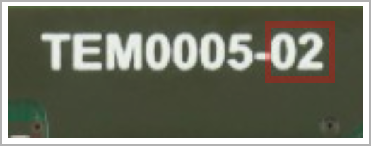
Hardware revision number can be found on the PCB board together with the module model number separated by the dash.
| Scroll Title |
|---|
| anchor | Figure_RV_HRN |
|---|
| title | Board hardware revision number. |
|---|
|
| Scroll Ignore |
|---|
| draw.io Diagram |
|---|
| border | false |
|---|
| |
|---|
| diagramName | TEM0005_RV_HRN |
|---|
| simpleViewer | false |
|---|
| width | 200 |
|---|
| links | auto |
|---|
| tbstyle | hidden |
|---|
| diagramDisplayName | |
|---|
| lbox | true |
|---|
| diagramWidth | 641175 |
|---|
| revision | 56 |
|---|
|
|
| Scroll Only |
|---|
Image Removed Image Added Image Added |
|
Document Change History
...