The Trenz Electronic TE0xxx-xx ... is an industrial-grade ... module ... based on Xilinx ...CR00040-01 is an CRUVI peripheral module with multiple sensors
Refer to http://trenz.org/tec0850cr00040-info for the current online version of this manual and other available documentation.
...
Page properties
hidden
true
id
Comments
Note: 'description: Important components and connector or other Features of the module → please sort and indicate assembly options
Key Features' must be split into 6 main groups for modules and mainboards:
SoC/FPGA
Package: SFVC784
Device: ZU2...ZU5*
Engine: CG, EG, EV*
Speed: -1LI, -2LE,*, **
Temperature: I, E,*, **
RAM/Storage
Low Power DDR4 on PS
Data width: 32bit
Size: def. 2GB*
Speed:***
eMMC
Data width: 8Bit
size: def. 8GB *
QSPI boot Flash in dual parallel mode (size depends on assembly version)
Data width: 8bit
size: def. 128MB *
HyperRAM/Flash (optional, default not assembled)
size:*
MAC address serial EEPROM with EUI-48™ node identity (Microchip 24AA025E48)
Hi-speed USB2 ULPI transceiver with full OTG support (Microchip USB3320C)
Interface
132 x HP PL I/Os (3 banks)
ETH
USB
4 GTR (for USB3, Sata, PCIe, DP)
MIO for UART
MIO for SD
MIO for PJTAG
JTAG
Ctrl
Power
3.3V-5V Main Input
3.3V Controller Input
Variable Bank IO Power Input
Dimension
4 cm x 5 cm
Notes
* depends on assembly version
** also non low power assembly options possible
*** depends on used U+ Zynq and DDR4 combination
Key Features' must be split into 6 main groups for carrier:
Modules
TE0808, TE807, TE0803,...
RAM/Storage
E.g. SDRAM, SPI
On Board
E.g. CPLD, PLL
Interface
E.g. ETH, USB, B2B, Display port
Power
E.g. Input supply voltage
Dimension
Excerpt
EEPROM/Unique Identifier
24AA025E48
CO2 Sensor (temperatur/humidity)
SCD40 or SCD41 or none (depending on assembly variant)
Air Pressure Sensor
LPS22HB
Ambient Light Sensor
TSL25403M
On-board
RGB LED
Buzzer
Power
3.3V
Dimension
32 x 18 mm
<Replace for module use "SoC/FPGA" for Carrier "Modules">
...
RAM/Storage
...
On Board
...
Interface
...
Power
...
Dimension
...
Notes
...
Block Diagram
Page properties
hidden
true
id
Comments
add drawIO object here.
Note
For more information regarding how to draw a diagram, Please refer to "Diagram Drawing Guidline" .
...
Scroll Title
anchor
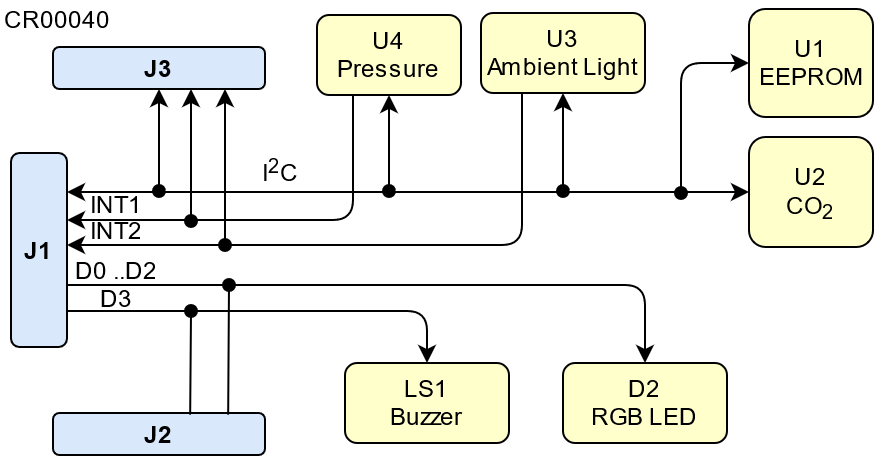
Figure_OV_BD
title
TExxxx CR00040 block diagram
Scroll Ignore
draw.io Diagram
border
false
diagramName
CR00040_OV_BD
simpleViewer
false
width
links
auto
tbstyle
top
diagramDisplayName
lbox
false
diagramWidth
437
revision
3
Scroll Only
Image Added
Create DrawIO object here: Attention if you copy from other page, objects are only linked.
Scroll Only
image link to the generate DrawIO PNG file of this page. This is a workaround until scroll pdf export bug is fixed
Main Components
Page properties
hidden
true
id
Comments
Notes :
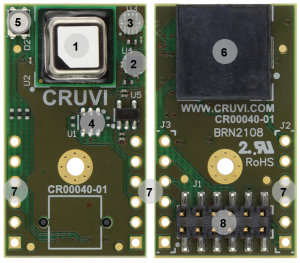
Picture of the PCB (top and bottom side) with labels of important components
Add List below
Note
For more information regarding how to add board photoes, Please refer to "Diagram Drawing Guidline" .
...
Scroll Title
anchor
Figure_OV_MC
title
TExxxx CR00040 main components
Scroll Ignore
Create DrawIO object here: Attention if you copy from other page, objects are only linked.
Scroll Only
image link to the generate DrawIO PNG file of this page. This is a workaround until scroll pdf export bug is fixed
...
...
...
Initial Delivery State
draw.io Diagram
border
false
diagramName
CR00040_OV_MC
simpleViewer
false
width
links
auto
tbstyle
top
diagramDisplayName
lbox
false
diagramWidth
358
revision
3
Scroll Only
Image Added
CO2 Sensor (not fitted on CR00040-XX-0)
Air Pressure Sensor
Ambient Light Sensor
EEPROM
RGB LED
Buzzer
Pin Headers (not fitted)
CRUVI Low Speed Connector
Initial Delivery State
Page properties
hidden
true
Page properties
hidden
true
id
Comments
Notes :
Only components like EEPROM, QSPI flash can be initialized by default at manufacture.
If there is no components which might have initial data ( possible on carrier) you must keep the table empty
...
Scroll Title
anchor
Table_OV_IDS
title
Initial delivery state of programmable devices on the module
Scroll Table Layout
orientation
portrait
sortDirection
ASC
repeatTableHeaders
default
style
widths
sortByColumn
1
sortEnabled
false
cellHighlighting
true
Storage device name
Content
Notes
Quad SPI Flash
EEPROM
System Controller CPLD
...
EEPROM
EUI-48 Node Identity
at offset 0xFA, 6 bytes
Signals, Interfaces and Pins
Page properties
hidden
true
id
Comments
Overview of Boot Mode, Reset, Enables.
Scroll Title
anchor
Table_OV_CNTRL
title
Controller signal.
Scroll Table Layout
orientation
portrait
sortDirection
ASC
repeatTableHeaders
default
style
widths
sortByColumn
1
sortEnabled
false
cellHighlighting
true
Name
Connector Pin
Direction
Description
Boot Mode
J1-2
input
high- SD low -QSPI
Enable
J1-3
input
..
Reset
JTAGSEL
PGOOD
...
Signals, Interfaces and Pins
Page properties
hidden
true
id
Comments
Notes :
For carrier or stand-alone boards use subsection for every connector type (add designator on description, not on the subsection title), for example:
SD
USB
ETH
FMC
...
For modules which needs carrier use only classes and refer to B2B connector if more than one is used, for example
JTAG
UART
I2C
MGT
...
Board to Board (B2B) I/Os
FPGA bank number and number of I/O signals connected to the B2B connector:
...
anchor
Table_SIP_B2B
title
General PL I/O to B2B connectors information
...
Notes :
For carrier or stand-alone boards use subsection for every connector type (add designator on description, not on the subsection title), for example:
SD
USB
ETH
FMC
...
For modules which needs carrier use only classes and refer to B2B connector if more than one is used, for example
JTAG
UART
I2C
MGT
...
Module I/Os
Module signals connected to the B2B connector:
Scroll Title
anchor
Table_SIP_B2B
title
General PL I/O to B2B connectors information
Scroll Table Layout
orientation
portrait
sortDirection
ASC
repeatTableHeaders
default
style
widths
sortByColumn
1
sortEnabled
false
cellHighlighting
true
B2B Connector
I/O Signal Count
Voltage Level
Notes
J1
8
VCC (3.3V)
J2
4
parallel to J1
J3
4
parallel to J1
J1 is the main CRUVI connector and should be used to connect the CR00040 to any CRUVI baseboard with CRUVI LS connector fitter. J2 and J2 are un-populated 100 mil pin-headers that allow solder-in pin-headers to use the CR00040 with solder-less breadboards or fly-wires.
On-board Peripherals
Page properties
hidden
true
id
Comments
Notes :
add subsection for every component which is important for design, for example:
Two 100 Mbit Ethernet Transciever PHY
USB PHY
Programmable Clock Generator
Oscillators
eMMCs
RTC
FTDI
...
DIP-Switches
Buttons
LEDs
Page properties
hidden
true
id
Comments
Notes :
In the on-board peripheral table "chip/Interface" must be linked to the corresponding chapter or subsection
Scroll Title
anchor
Table_SIP_JTGOBP
title
JTAG pins connectionOn board peripherals
Scroll Table Layout
orientation
portrait
sortDirection
ASC
repeatTableHeaders
default
style
widths
sortByColumn
1
sortEnabled
false
cellHighlighting
true
JTAG Signal
B2B Connector
TMS
TDI
TDO
TCK
JTAG_EN
On-board Peripherals
Page properties
hidden
true
id
Comments
Notes :
add subsection for every component which is important for design, for example:
Two 100 Mbit Ethernet Transciever PHY
USB PHY
Programmable Clock Generator
Oscillators
eMMCs
RTC
FTDI
...
DIP-Switches
Buttons
LEDs
Page properties
hidden
true
id
Comments
Notes :
In the on-board peripheral table "chip/Interface" must be linked to the corresponding chapter or subsection
Chip/Interface
Designator
Notes
EEPROM
U1
CO2 Sensor
U2
Ambient Light Sensor
U3
Pressure Sensor
U4
RGB LED
D2
Buzzer
LS1
Air Pressure Sensor
Scroll Title
anchor
Table_OBP_PRESS
title
Air Pressure Sensor interface pins
Scroll Table Layout
orientation
portrait
Scroll Title
anchor
Table_OBP
title
On board peripherals
Scroll Table Layout
orientation
portrait
sortDirection
ASC
repeatTableHeaders
default
style
widths
sortByColumn
1
sortEnabled
false
cellHighlighting
true
Chip/Interface
Designator
Notes
EEPROM
U1
CO2 Sensor
U2
Ambient Light Sensor
U3
Pressure Sensor
U4
RGB LED
D2
Buzzer
LS1
Quad SPI Flash Memory
...
hidden
true
id
Comments
Notes :
...
J1 Pin
Schematic
U4 Pin
Notes
2
SCL
2
1
SDA
4
Scroll Title
anchor
Table_OBP_I2C_PRESS
title
I2C address for Air Pressure Sensor
Scroll Table Layout
orientation
portrait
sortDirection
ASC
repeatTableHeaders
default
style
widths
sortByColumn
1
sortEnabled
false
cellHighlighting
true
I2C Address
Designator
Notes
1011_101x
U4
Ambient Light Sensor
Scroll Title
anchor
Table_OBP_SPIALS
title
Quad SPI interface MIOs and Ambient Light Sensor interface pins
Scroll Table Layout
orientation
portrait
sortDirection
ASC
repeatTableHeaders
default
style
widths
sortByColumn
1
sortEnabled
false
cellHighlighting
true
MIO
J1 Pin
Schematic
U??
U3 Pin
Notes
...
2
SCL
3
1
SDA
4
Scroll Title
anchor
Table_OBP_RTCI2C_ALS
title
I2C interface MIOs and pinsaddress for Ambient Light Sensor
Scroll Table Layout
orientation
portrait
sortDirection
ASC
repeatTableHeaders
default
style
widths
sortByColumn
1
sortEnabled
false
cellHighlighting
true
MIO Pin
Schematic
U? Pin
Notes
I2C Address
Designator
Notes
0111_001x
U3
CO2 Sensor
Scroll Title
anchor
Table_OBP_I2C_RTCEEP
title
I2C Address for RTCEEPROM interface pins
Scroll Table Layout
orientation
portrait
sortDirection
ASC
repeatTableHeaders
default
style
widths
sortByColumn
1
sortEnabled
false
cellHighlighting
true
MIO
J1 Pin
I2C Address
Schematic
Designator
U2 Pin
Notes
...
2
SCL
9
1
SDA
10
Scroll Title
anchor
Table_OBP_EEPI2C_EEPROM
title
I2C address for EEPROMinterface MIOs and pins
Scroll Table Layout
orientation
portrait
sortDirection
ASC
repeatTableHeaders
default
style
widths
sortByColumn
1
sortEnabled
false
cellHighlighting
true
MIO Pin
I2C Address
Schematic
U?? Pin
Notes
Designator
Notes
1100_010x
U2
EEPROM
Scroll Title
anchor
Table_OBP_I2C_EEPROMEEP
title
I2C address for EEPROM interface pins
Scroll Table Layout
orientation
portrait
sortDirection
ASC
repeatTableHeaders
default
style
widths
sortByColumn
1
sortEnabled
false
cellHighlighting
true
MIO
J1 Pin
I2C Address
Schematic
Designator
U1 Pin
Notes
...
2
SCL
1
1
SDA
3
Scroll Title
anchor
Table_OBP_LEDI2C_EEPROM
title
On-board LEDsI2C address for EEPROM
Scroll Table Layout
orientation
portrait
sortDirection
ASC
repeatTableHeaders
default
style
widths
sortByColumn
1
sortEnabled
false
cellHighlighting
true
I2C Address
Designator
Color
Connected to
Active Level
Note
DDR3 SDRAM
Page properties
hidden
true
id
Comments
Notes :
Minimum and Maximum density of DDR3 SDRAM must be mentioned for other assembly options. (pay attention to supported address length for DDR3)
The TE???? SoM has ??? GByte volatile DDR3 SDRAM IC for storing user application code and data.
Part number:
Supply voltage:
Speed:
NOR Flash
Temperature:
Ethernet
...
anchor
Table_OBP_ETH
title
Ethernet PHY to Zynq SoC connections
...
Notes
1010_011x
U1
LEDs
Scroll Title
anchor
Table_OBP_LED
title
On-board LEDs
Scroll Table Layout
orientation
portrait
sortDirection
ASC
repeatTableHeaders
default
style
widths
sortByColumn
1
sortEnabled
false
cellHighlighting
true
Designator
Color
Connected to
Active Level
Note
D2
Red
D0
Low
D2
Green
D1
Low
D2
Blue
D2
Low
Power and Power-On Sequence
Page properties
hidden
true
id
Comments
In 'Power and Power-on Sequence' section there are three important digrams which must be drawn:
Power on-sequence
Power distribution
Voltage monitoring circuit
Note
For more information regarding how to draw diagram, Please refer to "Diagram Drawing Guidline" .
Power Supply
Power supply with minimum current capability of TBD A is recommended.
Power Consumption
Scroll Title
anchor
Table_OBPPWR_CANPC
title
CAN Tranciever interface MIOsPower Consumption
Scroll Table Layout
orientation
portrait
sortDirection
ASC
repeatTableHeaders
default
style
widths
sortByColumn
1
sortEnabled
false
cellHighlighting
true
Bank
Schematic
U??
Power Input Pin
Notes
D-Tx
Driver Input
R-Rx
Reciever Output
...
Typical Current
VCC
TBD*
VBUS
0 (not used)
* TBD - To Be Determined
Power Distribution Dependencies
Scroll Title
anchor
TableFigure_OBPPWR_CLKPD
title
OsillatorsPower Distribution
scroll-
tablelayout
ignore
orientation
draw.io Diagram
portrait
border
sortDirection
false
ASC
repeatTableHeaders
default
style
widths
sortByColumn
1
sortEnabled
false
cellHighlighting
true
Designator
Description
Frequency
Note
MHz
MHz
KHz
Programmable Clock Generator
There is a programmable clock generator on-board (U??) provided in order to generate variable clocks for the module. Programming can be done using I2C via PIN header J??. The I2C Address is 0x??.
diagramName
CR00040_PWR_PD
simpleViewer
false
width
links
auto
tbstyle
top
diagramDisplayName
lbox
false
diagramWidth
405
revision
2
Scroll Only
Image Added
Power Rails
Scroll Title
anchor
Table_OBPPWR_PCLKPR
title
Programmable Clock Generator Inputs and OutputsModule power rails.
Scroll Table Layout
orientation
portrait
sortDirection
ASC
repeatTableHeaders
default
style
widths
sortByColumn
1
sortEnabled
false
cellHighlighting
true
Power Rail Name
B2B Connector
J1 Pin
B2B Connector
J2 Pin
B2B Connector
J3 Pin
U?? Pin
Signal
Connected to
Direction
Note
Notes
IN0
VCC
IN1
10
IN2
1
IN3
-
XAXB
in
SCLK
VBUS
SDA
12
OUT0
-
OUT1
1
OUT2
OUT3
OUT4
OUT5
OUT6
OUT7
OUT8/OUT9
Power and Power-On Sequence
n/a
not used
Board to Board Connectors
Page properties
hidden
Page properties
hidden
true
id
Comments
In 'Power and Power-on Sequence' section there are three important digrams which must be drawn:
Power on-sequence
Power distribution
Voltage monitoring circuit
Note
For more information regarding how to draw diagram, Please refer to "Diagram Drawing Guidline" .
Power Supply
Power supply with minimum current capability of xx A for system startup is recommended.
...
This section is optional and only for modules.
use "include page" macro and link to the general B2B connector page of the module series,
CR00040 module uses one Samtec connector at the bottom side.
1 x TMMH-106-04-F-DV-A-M (12 pins, 6 per row)
Operating Temperature: -55°C ~ 105°C Current Rating: 4.5A per Contact Number of Positions: 6 (2 x 6) Number of Rows: 2
Technical Specifications
Absolute Maximum Ratings
Scroll Title
anchor
Table_PWRTS_PCAMR
title
Power ConsumptionAbsolute maximum ratings
Scroll Table Layout
orientation
portrait
sortDirection
ASC
repeatTableHeaders
default
style
widths
sortByColumn
1
sortEnabled
false
cellHighlighting
true
Power Input Pin
Typical Current
VIN
TBD*
* TBD - To Be Determined
Power Distribution Dependencies
...
anchor
Figure_PWR_PD
title
Power Distribution
Scroll Ignore
Create DrawIO object here: Attention if you copy from other page, objects are only linked.
Scroll Only
image link to the generate DrawIO PNG file of this page. This is a workaround until scroll pdf export bug is fixed
Symbols
Description
Min
Max
Unit
VCC
Main Power
-0.3
4.8
V
VBUS
n/a
n/a
V
SDA, SCL
-0.3
3.6
V
INT1
-0.3
VCC+0.3
V
INT2
-0.3
3.6
V
D0, D1, D2
-5
3.6
V
D3
-25*
25
V
Operating Temperature
-10
60
°C
Recommended Operating Conditions
Operating temperature range depends also on customer design and cooling solution. Please contact us for options.
Scroll Title
anchor
Table_TS_ROC
title
Recommended operating conditions.
Scroll Table Layout
orientation
portrait
sortDirection
Power-On Sequence
...
anchor
Figure_PWR_PS
title
Power Sequency
Scroll Ignore
Create DrawIO object here: Attention if you copy from other page, objects are only linked.
Scroll Only
image link to the generate DrawIO PNG file of this page. This is a workaround until scroll pdf export bug is fixed
Voltage Monitor Circuit
...
anchor
Figure_PWR_VMC
title
Voltage Monitor Circuit
Scroll Ignore
Create DrawIO object here: Attention if you copy from other page, objects are only linked.
Scroll Only
image link to the generate DrawIO PNG file of this page. This is a workaround until scroll pdf export bug is fixed
Power Rails
Scroll Title
anchor
Table_PWR_PR
title
Module power rails.
Scroll Table Layout
orientation
portrait
sortDirection
ASC
repeatTableHeaders
default
style
widths
sortByColumn
1
sortEnabled
false
cellHighlighting
true
Power Rail Name
B2B Connector
JM1 Pin
B2B Connector
JM2 Pin
B2B Connector
JM3 Pin
Direction
Notes
Bank Voltages
...
anchor
Table_PWR_BV
title
Zynq SoC bank voltages.
...
Bank
...
Voltage
...
hidden
true
id
Comments
...
Parameter
Min
Typ
Max
Units
Reference Document
VCC
2.4
3.3
3.6
V
See LPS22HBTR datasheet.
VBUS
n/a
n/a
n/a
V
not used
Storage Temperature
10
-
50
°C
See SCD40 datasheet.
Short term storage Temperature
-40
-
70
°C
See SCD40 datasheet.
Operating Temperature
-10
-
60
°C
See SCD40 datasheet.
Physical Dimensions
Module size: 32 mm × 18 mm. Please download the assembly diagram for exact numbers.
Mating height with standard connectors: 5 mm.
PCB thickness: 1.6 mm.
Page properties
hidden
true
id
Comments
In 'Physical Dimension' section, top and bottom view of module must be inserted, information regarding physical dimensions can be obtained through webpage for product in Shop.Trenz, (Download> Documents> Assembly part) for every SoM.
For Example: for Module TE0728, Physical Dimension information can be captured by snipping tools from the link below:
3 x REF-??????? (compatible to ????????), (?? pins, ?? per row)
Operating Temperature: -??°C ~ ??°C Current Rating: ??A per ContactNumber of Positions: ?? Number of Rows: ??
Technical Specifications
Absolute Maximum Ratings
...
anchor
Table_TS_AMR
title
PS absolute maximum ratings
...
Recommended Operating Conditions
Operating temperature range depends also on customer design and cooling solution. Please contact us for options.
...
anchor
Table_TS_ROC
title
Recommended operating conditions.
...
Physical Dimensions
Module size: ?? mm × ?? mm. Please download the assembly diagram for exact numbers.
Mating height with standard connectors: ? mm.
PCB thickness: ?? mm.
Page properties
hidden
true
id
Comments
In 'Physical Dimension' section, top and bottom view of module must be inserted, information regarding physical dimensions can be obtained through webpage for product in Shop.Trenz, (Download> Documents> Assembly part) for every SoM.
For Example: for Module TE0728, Physical Dimension information can be captured by snipping tools from the link below:
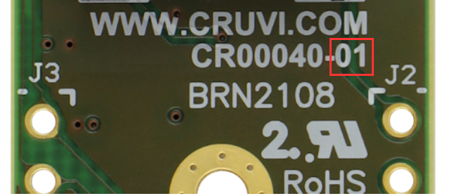
Hardware revision number can be found on the PCB board together with the module model number separated by the dash.
Scroll Title
anchor
Figure_RV_HRN
title
Board hardware revision number..
Scroll Ignore
draw.io Diagram
border
false
diagramName
CR00040_HRN
simpleViewer
false
width
links
auto
tbstyle
top
diagramDisplayName
lbox
false
diagramWidth
214
revision
2
Scroll Only
Image Added
Scroll Ignore
Create DrawIO object here: Attention if you copy from other page, objects are only linked.
Scroll Only
image link to the generate DrawIO PNG file of this page. This is a workaround until scroll pdf export bug is fixed
Document Change History
Page properties
hidden
true
id
Comments
Note this list must be only updated, if the document is online on public doc!
It's semi automatically, so do following
Add new row below first
Copy "Page Information Macro(date)" Macro-Preview, Metadata Version number, Author Name and description to the empty row. Important Revision number must be the same as the Wiki document revision number Update Metadata = "Page Information Macro (current-version)" Preview+1 and add Author and change description. --> this point is will be deleted on newer pdf export template
Metadata is only used of compatibility of older exports