| Page properties |
|---|
|
Template Revision 3.1
- Module: TRM Name always "TE Series Name" +TRM
Example: "TE0728 TRM"
Template Change history: Template Change history: - 3.02 to 3.1
- New general notes for temperature range to "Recommended Operating Conditions"
- 3.01 to 3.02
- add again fix table of content with workaround to use it for pdf and wiki
- Export Link for key features examples
- Notes for different Types (with and without Main FPGA)
- Export Link for Signals, Interfaces and Pins examples
- Notes for different Types (Modul, Modul Hypride, Evalboard, Carrier)
- 3.0 to 3.01
- remove fix table of content and page layout ( split page layout make trouble with pdf export)
- changed and add note to signal and interfaces, to on board periphery section
- ...(not finished)
- 2.13 to 3.00
- → separation of Carrier/Module and evaluation kit TRM
- 2.14 to 2.15
- add excerpt macro to key features
- 2.13 to 2.14
- add fix table of content
- add table size as macro
|
| Page properties |
|---|
|
Important General Note:
|
| Page properties |
|---|
|
----------------------------------------------------------------------- |
| Page properties |
|---|
|
Note for Download Link of the Scroll ignore macro: |
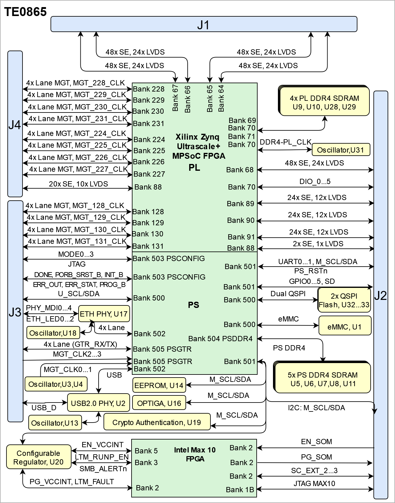
Overview
The Trenz Electronic TE0865 is a high-performance MPSoC module integrating a Xilinx Zynq UltraScale+ ZU17EG (other assembly options for the FPGA are available), up to 8 GByte DDR4 SDRAM with ECC on PS, up to 8 GByte DDR4 SDRAM on PL, 256 MByte Flash memory for configuration and operation, Gigabit Ethernet PHY, and powerful switch-mode power supplies for all on-board voltages. A large number of configurable I/O's is provided via rugged high-speed stacking connections.
The prototype configuration of TE0865 will be available with many configuration options available that you can customize to meet your specific needs.
All parts are at least extended temperature range of 0°C to +85°C. The module operating temperature range depends on customer design and cooling solution. Please contact us for options.
Refer to http://trenz.org/te0865-info for the current online version of this manual and other available documentation.
Key Features
| Excerpt |
|---|
- SoC/FPGA
- Package: C1760
- Device: ZU11, ZU17, ZU19*
- Engine: EG*
- Speed: -1, -2,*, **
- Temperature: I, E,*, **
- RAM/Storage
- DDR4 on PS with ECC
- Data width: 64 bit
- Size: def. 4GB*
- Speed: 2400 (Gb/s) ***
- DDR4 on PL
- Data width: 64 bit
- Size: def. 4GB*
- Speed: max 2666 (Gb/s) ***
- eMMC
- Data width: 8 Bit
- size: def. 8 GB *
- Dual QSPI boot Flash in dual parallel mode (size depends on assembly version)
- Data width: 8bit
- size: def. 64MB *
- MAC address serial EEPROM with EUI-48™ node identity (Microchip 24AA025E48)
- On Board
- Intel Max 10 FPGA as CPLD
- 6x MEMS Oscillator
- Gigabit Ethernet transceiver PHY (Marvell Alaska 88E1512)
- Hi-speed USB2 ULPI transceiver with full OTG support (Microchip USB3340C)
- Interface
- 96 HD I/Os
- 240 HP I/Os
- 4x PS GTR
- 3x Samtec Accelerate HD B2B connector
- 21 MIOs
- Power
- 12V input supply voltage
- Variable Bank IO Power Input
- Dimension
- Notes
- * depends on assembly version
- ** also non low power assembly options possible
- *** depends on used U+ Zynq and DDR4 combination
|
Block Diagram
| Page properties |
|---|
|
add drawIO object in Scroll Ignore section and add reference image in Scroll Only.
| Note |
|---|
Title (not anchor) of all Scroll Title such as DrawIOs and Tables should be changed according to the Module name. Example: TE0812 Block Diagram |
| Note |
|---|
All created DrawIOs should be named according to the Module name: Example: DrawIO of TE0812 Block Diagram should be named TE0812_OV_BD |
|
| Scroll Title |
|---|
| anchor | Figure_OV_BD |
|---|
| title | TE0865 block diagram |
|---|
|
| Scroll Ignore |
|---|
| draw.io Diagram |
|---|
| border | false |
|---|
| |
|---|
| diagramName | TE0865_OV_BD |
|---|
| simpleViewer | false |
|---|
| width | |
|---|
| links | auto |
|---|
| tbstyle | hidden |
|---|
| diagramDisplayName | |
|---|
| lbox | true |
|---|
| diagramWidth | 641 |
|---|
| revision | 35 |
|---|
|
|
| Scroll Only |
|---|
|
|
Main Components
| Page properties |
|---|
|
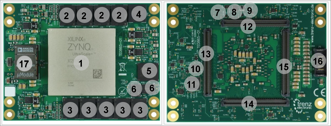
Notes : - Picture of the PCB (top and bottom side) with labels of important components
- Add List below
|
| Scroll Title |
|---|
| anchor | Figure_OV_MC |
|---|
| title | TE0865 main components |
|---|
|
| Scroll Ignore |
|---|
| draw.io Diagram |
|---|
| border | false |
|---|
| |
|---|
| diagramName | TE0865_OV_MC |
|---|
| simpleViewer | false |
|---|
| width | |
|---|
| links | auto |
|---|
| tbstyle | hidden |
|---|
| diagramDisplayName | |
|---|
| lbox | true |
|---|
| diagramWidth | 641 |
|---|
| revision | 13 |
|---|
|
|
| Scroll Only |
|---|
|
|
- ZYNQ Ultrascale+ MPSoC FPGA, U30
- PL DDR4 SDRAM, U9, U10, U28, U29
- PS DDR4 SDRAM, U5...U8, U11
- Intel MAX 10 FPGA, U46
- eMMC RAM, U1
- Dual QSPI Flash, U32, U33
- Crypto Authentication IC, U19
- OPTIGA Trust M Authentication IC, U16
- EEPROM MAC Address, U14
- USB2.0 Transceiver, U2
- Gigabit Ethernet Transceiver, U17
- B2B Connector, J2
- B2B Connector, J3
- B2B Connector, J1
- B2B Connector, J4
- Power Terminal, J5
- Configurable Regulator, U20
Initial Delivery State
| Page properties |
|---|
|
| Note |
|---|
Only components like EEPROM, QSPI flash can be initialized by default at manufacture. If there is no components which might have initial data ( possible on carrier) you must keep the table empty |
|
| Scroll Title |
|---|
| anchor | Table_OV_IDS |
|---|
| title | Initial delivery state of programmable devices on the module |
|---|
|
| Scroll Table Layout |
|---|
| orientation | portrait |
|---|
| sortDirection | ASC |
|---|
| repeatTableHeaders | default |
|---|
| style | |
|---|
| widths | |
|---|
| sortByColumn | 1 |
|---|
| sortEnabled | false |
|---|
| cellHighlighting | true |
|---|
|
Storage device name | Content | Notes |
|---|
Quad SPI Flash | Not Programmed |
| | EEPROM | Programmed | MAC Address | | System Controller CPLD | Programmed | Intel MAX 10 | | PL DDR4 SDRAM | Not Programmed |
| | PS DDR4 SDRAM | Not Programmed |
| | eMMC | Not Programmed |
|
|
Configuration Signals
| Page properties |
|---|
|
- Overview of Boot Mode, Reset, Enables.
|
| Scroll Title |
|---|
| anchor | Table_OV_CNTRL |
|---|
| title | Controller signal. |
|---|
|
| Scroll Table Layout |
|---|
| orientation | portrait |
|---|
| sortDirection | ASC |
|---|
| repeatTableHeaders | default |
|---|
| style | |
|---|
| widths | |
|---|
| sortByColumn | 1 |
|---|
| sortEnabled | false |
|---|
| cellHighlighting | true |
|---|
|
Function | Schematic | Connected to | Direction | Description |
|---|
Boot Mode | MODE0...3 | B2B, J3A | Input |
| | Reset | PERST0 | B2B, J1B | Input |
| | Power Good | PG_SOM | B2B, J2B | Output |
| | Power Enable | EN_SOM | B2B, J2B | Input |
| | Manual Reset | MR | B2B, J2B CPLD, U46 | Output Output |
| | Power Signal | PG_+3.3V | B2B, J2B | Output |
| | Battery Supply | V_BAT | Bank PSCONFIG | Input |
| | Control Signal | DONE | B2B, J3B | Output | Pull up | | Control Signal | POR_B | B2B, J3B | Input | Pull up | | Initialization Signal | INIT_B | B2B, J3B | Output | Pull up | | Program Signal | PROG_B | B2B, J3B | Output | Pull up | | Reset Signal | SRST_B | B2B, J3B | Input | Pull up |
|
Signals, Interfaces and Pins
Board to Board (B2B) I/Os
FPGA bank number and number of I/O signals connected to the B2B connector:
| Scroll Title |
|---|
| anchor | Table_SIP_B2B |
|---|
| title | General PL I/O to B2B connectors information |
|---|
|
| Scroll Table Layout |
|---|
| orientation | portrait |
|---|
| sortDirection | ASC |
|---|
| repeatTableHeaders | default |
|---|
| style | |
|---|
| widths | |
|---|
| sortByColumn | 1 |
|---|
| sortEnabled | false |
|---|
| cellHighlighting | true |
|---|
|
| Bank | Type | B2B Connector | I/O Signal Count | Voltage | Notes |
|---|
64 | HP | JM2 | 48x Single Ended, 24x LVDS Pairs | Variable | Max voltage 1.8V | | 65 | HP | JM2 | 24x Single Ended, 12x LVDS Pairs | Variable | Max voltage 1.8V | 65 | HP | JM3 | 24x Single Ended, 12x LVDS Pairs | Variable | Max voltage 1.8V | 66 | HP | JM1 | 48x Single Ended, 24x LVDS Pairs | Variable | Max voltage 1.8V | | 500 | MIO | JM1 | 26x Single Ended | 1.8V | MIO0...25 | 501 | MIO | JM1 | 6x Single Ended | Variable | Max voltage 3.3V | 505 | GTR | JM3 | 16x Single Ended, 8x LVDS Pairs | 0.85V | 4x Lanes | 505 | GTR CLK | JM3 | 2x differential Clock | - |
|
|
For detailed information about the pin-out, please refer to the Pin-out table.
MGT Lanes
The Xilinx Zynq UltraScale+ device used on the TE0865 module has 4x Lanes MGT transceivers connected to Bank 505 PSGTR. All 4x lanes are wired directly to B2B connector J3B consisting of one transmit and one receive (TX/RX) differential pairs, four signals total per one MGT lane. Furthuremore, MGT clocks are sourced by oscillators U3 and U4 at 27 and 100 MHz respectively.
Following table lists lane number, FPGA bank number, transceiver type, signal schematic name, board-to-board pin connection and FPGA pins connection:
| Scroll Title |
|---|
| anchor | Table_SIP_MGT |
|---|
| title | MGT Lanes connection |
|---|
|
| Scroll Table Layout |
|---|
| orientation | portrait |
|---|
| sortDirection | ASC |
|---|
| repeatTableHeaders | default |
|---|
| style | |
|---|
| widths | |
|---|
| sortByColumn | 1 |
|---|
| sortEnabled | false |
|---|
| cellHighlighting | true |
|---|
|
| Bank | Pin | Signal Name | B2B Pin | Note |
|---|
505
(PSGTR)
| MGT Lane 0 | - GTR_RX0_P
- GTR_RX0_N
- GTR_TX0_P
- GTR_TX0_N
| - J3B-D39
- J3B-D40
- J3B-C38
- J3B-C39
|
| | MGT Lane 1 | - GTR_RX1_P
- GTR_RX1_N
- GTR_TX1_P
- GTR_TX1_N
| - J3B-D36
- J3B-D37
- J3B-C35
- J3B-C36
|
| | MGT Lane 2 | - GTR_RX2_P
- GTR_RX2_N
- GTR_TX2_P
- GTR_TX2_N
| - J3B-D33
- J3B-D34
- J3B-C32
- J3B-C33
|
| | MGT Lane 3 | - GTR_RX3_P
- GTR_RX3_N
- GTR_TX3_P
- GTR_TX3_N
| - J3B-D30
- J3B-D31
- J3B-C29
- J3B-C30
|
| | MGT_CLK0 | MGT505_CLK0 (P/N) | Oscillator, U3 | 27 MHz | | MGT_CLK1 | MGT505_CLK1 (P/N) | Oscillator, U4 | 100 MHz | | MGT_CLK2 | - MGT505_CLK2_P
- MGT505_CLK2_N
| |
| | MGT_CLK3 | - MGT505_CLK2_P
- MGT505_CLK2_N
| |
|
|
There are 3 clock sources for the GTR transceivers. B505_CLK0 is connected directly to B2B connector JM3, so the clock can be provided by the carrier board. Clocks B505_CLK1 and B505_CLK3 are provided by the on-board clock generator (U10). As there are no capacitive coupling of the data and clock lines that are connected to the connectors, these may be required on the user’s PCB depending on the application.JTAG Interface
JTAG access to the UltraScale+ MPsoC FPGA through B2B connector J3B.
| Scroll Title |
|---|
| anchor | Table_SIP_JTG |
|---|
| title | JTAG pins connection |
|---|
|
| Scroll Table Layout |
|---|
| orientation | portrait |
|---|
| sortDirection | ASC |
|---|
| repeatTableHeaders | default |
|---|
| style | |
|---|
| widths | |
|---|
| sortByColumn | 1 |
|---|
| sortEnabled | false |
|---|
| cellHighlighting | true |
|---|
|
JTAG Signal | B2B Connector |
|---|
| TMS | J3B- D59 | | TDI | J3B- D57 | | TDO | J3B- D58 | | TCK | J3B- D56 |
|
JTAG access to the system controller CPLD, Intel MAX10 FPGA(U46) through B2B connector J2B.
| Scroll Title |
|---|
| anchor | Table_SIP_JTG |
|---|
| title | JTAG pins connection |
|---|
|
| Scroll Table Layout |
|---|
| orientation | portrait |
|---|
| sortDirection | ASC |
|---|
| repeatTableHeaders | default |
|---|
| style | |
|---|
| widths | |
|---|
| sortByColumn | 1 |
|---|
| sortEnabled | false |
|---|
| cellHighlighting | true |
|---|
|
JTAG Signal | B2B Connector |
|---|
| TCK_MAX10 | J2B- D56 | | TMS_MAX10 | J2B- D57 | | TDO_MAX10 | J2B- D58 | | TDI_MAX10 | J2B- D59 | | JTAGEN | Pulled Up |
|
I2C Addresses
| Scroll Title |
|---|
| anchor | Table_SIP_I2CADD |
|---|
| title | I2C addresses |
|---|
|
| Scroll Table Layout |
|---|
| orientation | portrait |
|---|
| sortDirection | ASC |
|---|
| repeatTableHeaders | default |
|---|
| style | |
|---|
| widths | |
|---|
| sortByColumn | 1 |
|---|
| sortEnabled | false |
|---|
| cellHighlighting | true |
|---|
|
| I2C Address | Designator | Notes |
|---|
| 0x53 | U14 | EEPROM | | 0x30 | U16 | OPTIGA Trust M | | 0x4E | U20 | Configurable Regulator |
|
MIO Pins
| Page properties |
|---|
|
you must fill the table below with group of MIOs which are connected to a specific components or peripherals, you do not have to specify pins in B2B, Just mention which B2B is connected to MIOs. The rest is clear in the Schematic. Example: | MIO Pin | Connected to | B2B | Notes |
|---|
| MIO12...14 | SPI_CS , SPI_DQ0... SPI_DQ3 SPI_SCK | J2 | QSPI |
|
| Scroll Title |
|---|
| anchor | Table_SIP_MIOs |
|---|
| title | MIOs pins |
|---|
|
| Scroll Table Layout |
|---|
| orientation | portrait |
|---|
| sortDirection | ASC |
|---|
| repeatTableHeaders | default |
|---|
| style | |
|---|
| widths | |
|---|
| sortByColumn | 1 |
|---|
| sortEnabled | false |
|---|
| cellHighlighting | true |
|---|
|
| MIO Pin | Connected to | Notes |
|---|
| MIO0...5 | QSPI Flash, U32 |
| | MIO6...11 | QSPI, Flash, U33 |
| | MIO13...22 | eMMC, U1 |
| | MIO23 | B2B, J2A | U_INIT | | MIO24...25 | B2B, J3B | I2C via Voltage Transform, U15 | | MIO26...27 | B2B, J2A | UART0_RX | | MIO28...29 | B2B, J2A | UART1_RX | | MIO30...31 | B2B, J2A | I2C via Voltage Transform, U12 | | MIO32...37 | B2B, J2A | GPIO0...5 | | MIO38 | B2B, J2A | M_INIT | | MIO39...42 | B2B, J2B | SD | | MIO43 | B2B, J2A | PS_RSTn | | MIO44...51 | B2B, J2A | SD | | MIO52...63 | USB2.0, U2 | USB2.0 | | MIO64...77 | ETH PHY, U17 | ETH PHY |
|
Test Points
| Page properties |
|---|
|
you must fill the table below with group of Test Point which are indicated as TP in a schematic. If there is no Test Point remarked in the schematic, delet the Test Point section. Example: | Test Point | Signal | B2B | Notes |
|---|
| 10 | PWR_PL_OK | J2-120 |
|
|
| Scroll Title |
|---|
| anchor | Table_SIP_TPs |
|---|
| title | Test Points Information |
|---|
|
| Scroll Table Layout |
|---|
| orientation | portrait |
|---|
| sortDirection | ASC |
|---|
| repeatTableHeaders | default |
|---|
| style | |
|---|
| widths | |
|---|
| sortByColumn | 1 |
|---|
| sortEnabled | false |
|---|
| cellHighlighting | true |
|---|
|
| Test Point | Signal | Notes |
|---|
| TP1...2 | +12.0V |
| | TP3...4 | +3.3V |
| | TP5...6 | +3.3V_SW |
| | TP7...8 | +2.3V |
| | TP9...10 | +1.8V |
| | TP11...12 | +1.8V_AUX |
| | TP13...14 | +1.8V_VCCADC |
| | TP15...16 | +0.85V_VCCINT |
| | TP17...18 | +1.2V_PL_DDR |
| | TP19...20 | +2.5V_PL_DDR |
| | TP21...22 | +0.85V_GTR_AVCC_PS |
| | TP23...24 | +1.8V_GTR_AVTT_PS |
| | TP25...26 | +1.8V_AUX_PS |
| | TP27...28 | +1.2V_PLL_PS |
| | TP29...30 | +1.2V_PS_DDR |
| | TP31...32 | +2.5V_PS_DDR |
| | TP33...34 | VREFA_DDR_PS |
| | TP35...36 | VREFA_DDR_PL |
| | TP37...38 | VTT_DDR_PS |
| | TP39...40 | VTT_DDR_PL |
| | TP41...42 | +0.9V_GTH_AVCC |
| | TP43...44 | +1.8V_GTH_AUX |
| | TP45...46 | +1.2V_GTH_AVTT |
| | TP47...48 | +0.9V_GTY_AVCC |
| | TP49...50 | +1.8V_GTY_AUX |
| | TP51...52 | +1.2V_GTY_AVTT |
|
|
On-board Peripherals
| Page properties |
|---|
|
Notes : In the on-board peripheral table "chip/Interface" must be linked to the corresponding chapter or subsection by assigning advance link using: #NameOfTheSection Example: #ClockSources, #CPLD, #QuadSPIFlash |
| Scroll Title |
|---|
| anchor | Table_OBP |
|---|
| title | On board peripherals |
|---|
|
| Scroll Table Layout |
|---|
| orientation | portrait |
|---|
| sortDirection | ASC |
|---|
| repeatTableHeaders | default |
|---|
| style | |
|---|
| widths | |
|---|
| sortByColumn | 1 |
|---|
| sortEnabled | false |
|---|
| cellHighlighting | true |
|---|
|
| Chip/Interface | Designator | Notes |
|---|
| Intel MAX 10 CPLD | U46 |
| | PL DDR4 SDRAM | U9, U10, U28, U29 |
| | PS DDR4 SDRAM | U5...U8, U11 |
| | Dual QSPI Flash | U32, U33 |
| | eMMC Memory | U1 |
| | USB2.0 Transceiver | U2 |
| | Gigabit Ethernet Transceiver | U17 |
| | EEPROM | U14 |
| | Crypto Authentication | U19 |
| | OPTIGA Authentication | U16 |
| | MEMS Oscillator | U3, U4, U13, U18, U31, U34 |
|
|
System Controller CPLD
| Page properties |
|---|
|
| Note |
|---|
Link always to CPLD Documentation, because CPLD Firmware can be changed during the time. Describe used device type and basic Pin connection to B2B and Main FPGA |
|
The TE0865 is equipped with an Intel MAX 10 as System Controller CPLD (U46). Please check further information in the TE0865 CPLD page.
| Scroll Title |
|---|
| anchor | Table_OBP_CPLD |
|---|
| title | CPLD pin connections |
|---|
|
| Scroll Table Layout |
|---|
| orientation | portrait |
|---|
| sortDirection | ASC |
|---|
| repeatTableHeaders | default |
|---|
| style | |
|---|
| widths | |
|---|
| sortByColumn | 1 |
|---|
| sortEnabled | false |
|---|
| cellHighlighting | true |
|---|
|
| Bank | Schematic | Connectced to | Notes |
|---|
| Bank 1A | VCCIO1A | 3.3V |
| | Bank 1B | TCK_MAX10 | B2B, J2B |
| | TMS_MAX10 | B2B, J2B |
| | TDO_MAX10 | B2B, J2B |
| | TDI_MAX10 | B2B, J2B |
| | VCCIO1B | 3.3V |
| | Bank 2 | EN_VTT_DDR_PL | Regulator, U26 |
| | EN_+2.5V_PL_DDR | Regulator, U22 | Enable Power DDR4 PL | | EN_+1.2V_PL_DDR | Regulator, U24 | Enable Power DDR4 PL | | PG_+1.2V_PL_DDR | Regulator, U24 | Power Good DDR4 PL | | EN_+1.8V_AUX_PS | Regulator, U43 |
| | EN_SOM | B2B, J2B | Main 'Power Enable' signal | | PG_SOM | B2B, J2B | Main 'Power Good' signal | | SC_EXT_2...3 | B2B, J2B |
| | PG_VCCINT | Regulator, U20 | Configurable Regulator | | LTM_FAULT | Regulator, U20 | Configurable Regulator | | MR | B2B, J2B Regulator, U51 |
| | Bank 3 | SMB_ALERTn | Regulator, U20 | Configurable Regulator | | PG_+2.5V_PL_DDR | Regulator, U22 | Power Good DDR4 PL | | LTM_RUNP_EN | Regulator, U20 | Configurable Regulator | | M_SDA | I2C Bus | B2B, J2A via level shifter (U12) | | M_SCL | I2C Bus | B2B, J2A via level shifter (U12) | | RST_SYSn | Diod, U53B | Reset | | EN_+0.9V_GTH_AVCC | Regulator, U35 |
| | EN_+0.9V_GTY_AVCC | Regulator, U38 |
| | PG_+1.2V_PS_DDR | Regulator, U25 | Power Good DDR4 PS | | PG_+0.9V_GTH_AVCC | Regulator, U35 |
| | PG_+0.9V_GTY_AVCC | Regulator, U38 |
| | EN_+3.3V_SW | Regulator, U52 | Secondary Power | | EN_+1.2V_PLL_PS | Regulator, U42 |
| | PG_+1.8V_GTR_AVTT_PS | Regulator, U47 |
| | PG_+1.8V | Regulator, U41 |
| | EN_+2.5V_PS_DDR | Regulator, U23 | Enable Power DDR4 PS | | PG_+1.2V_GTY_AVTT | Regulator, U39 |
| | EN_+1.2V_GTY_AVTT | Regulator, U39 |
| | M_INT | B2B, J2A |
| | EN_+1.8V_VCCADC | Regulator, U49 |
| | PG_+0.85V_GTR_AVCC_PS | Regulator, U48 |
| | EN_VTT_DDR_PS | Regulator, U27 |
| | EN_+1.8V | Regulator, U41 |
| | EN_+1.8V_GTY_AUX | Regulator, U40 |
| | PG_+2.3V | Regulator, U45 |
| | Bank 6 | VCCIO6 | 3.3V |
| | Bank 5 | EN_+1.8V_GTR_AVTT_PS | Regulator, U47 |
| | EN_+1.8V_GTH_AUX | Regulator, U37 |
| | EN_+1.8V_AUX | Regulator, U50 |
| | EN_+1.2V_GTH_AVTT | Regulator, 36 |
| | PG_+1.2V_GTH_AVTT | regulator, U36 |
| | +3.3V_SW | eMMC, U1 |
| | EN_+1.2V_PS_DDR | Regulator, U25 | Power Good DDR4 PS | | EN_+0.85V_GTR_AVCC_PS | Regulator, U48 |
| | PG_+1.2V_GTH_AVTT | Regulator, U48 |
| | EN_VCCINT | Regulator, U20 |
| | EN_+2.3V | Regulator, U45 |
| | PG_+1.8V_AUX | Regulator, U50 |
| | PG_+2.5V_PS_DDR | Regulator, U23 | Power Good DDR4 PS |
|
Dual QSPI Flash Memory
| Page properties |
|---|
|
Notes : Minimum and Maximum density of quad SPI flash must be mentioned for other assembly options. |
The TE0865 is equipped with dual 128 Mb (256 Mb) QSPI flash memory, U32 and U33 for configuration and operation storage.
| Scroll Title |
|---|
| anchor | Table_OBP_SPI |
|---|
| title | Quad SPI interface MIOs and pins |
|---|
|
| Scroll Table Layout |
|---|
| orientation | portrait |
|---|
| sortDirection | ASC |
|---|
| repeatTableHeaders | default |
|---|
| style | |
|---|
| widths | |
|---|
| sortByColumn | 1 |
|---|
| sortEnabled | false |
|---|
| cellHighlighting | true |
|---|
|
| Designator | Pin | Schematic | Notes |
|---|
| U32 | CLK | MIO0 |
| | DI/IO0 | MIO4 |
| | DO/IO1 | MIO1 |
| | nWP/IO2 | MIO2 |
| | nHOLD/IO3 | MIO3 |
| | nCS | MIO5 |
| | U33 | CLK | MIO12 |
| | DI/IO0 | MIO8 |
| | DO/IO1 | MIO9 |
| | nWP/IO2 | MIO10 |
| | nHOLD/IO3 | MIO11 |
| | nCS | MIO7 |
|
|
eMMC Memory
The TE0865 is equipped with an eMMC Flash memory IC(U1) connected to the PS MIO pins MIO13..MIO22.
| Scroll Title |
|---|
| anchor | Table_OBP_eMMC |
|---|
| title | eMMC connections |
|---|
|
| Scroll Table Layout |
|---|
| orientation | portrait |
|---|
| sortDirection | ASC |
|---|
| repeatTableHeaders | default |
|---|
| style | |
|---|
| widths | |
|---|
| sortByColumn | 1 |
|---|
| sortEnabled | false |
|---|
| cellHighlighting | true |
|---|
|
| Designator | Pin | Schematic | Connected to | Notes |
|---|
| U32 | CLK | MMC-CCLK | MIO22 |
| | nRESET | RST_PERn | - | PS_RSTn, PS_SYSn | | CMD | MMC-CMD | MIO21 |
| | DAT0...7 | MMCD0...7 | MIO13...20 |
|
|
Gigabit Ethernet
On-board Gigabit Ethernet PHY (U17) is provided with Marvell Alaska 88E1512 IC (U17). The Ethernet PHY RGMII interface is connected to the ZynqMP Ethernet3 PS GEM3. I/O voltage is fixed at 1.8V for HSTL signaling. The reference clock input of the ETH is supplied from an on-board 25.00 MHz oscillator (U18).
| Scroll Title |
|---|
| anchor | Table_SIP_ETH |
|---|
| title | GigaBit Ethernet connection |
|---|
|
| Scroll Table Layout |
|---|
| orientation | portrait |
|---|
| sortDirection | ASC |
|---|
| repeatTableHeaders | default |
|---|
| style | |
|---|
| widths | |
|---|
| sortByColumn | 1 |
|---|
| sortEnabled | false |
|---|
| cellHighlighting | true |
|---|
|
| Pin | Schematic | Connected to | Note |
|---|
| MDIP0...3 | PHY_MDI0...3 | B2B, J3A |
| | MDC | ETH_MDC | MIO76 |
| | MDIO | ETH_MDIO | MIO77 |
| | S_IN | S_IN | N.C |
| | S_OUT | S_OUT | N.C |
| | TXD0..3 | ETH_TXD0...3 | MIO65...68 |
| | TX_CTRL | ETH_TXCTL | MIO69 |
| | TX_CLK | ETH_TXCK | MIO64 |
| | RXD0...3 | ETH_RXD0...3 | MIO71...74 |
| | RX_CTRL | ETH_RXCTL | MIO75 |
| | RX_CLK | ETH_RXCK | MIO70 |
| | LED1 | PHY_LED1 | B2B, J3A |
| | RESETn | ETH_RST | MIO24 |
| | XTAL_IN | ETH_CLK | Oscillator, U18 | Input Clock of ETH Transciever | | nRESET | RST_PERn | B2B, J2A | PS_RSTn, PS_SYSn |
|
USB2.0 Transceiver
Hi-speed USB2.0 transceiver (U2) is provided with USB3340 from Microchip. The transceiver is connected to the PS MIO via MIO52..63. The I/O voltage is fixed at 3.3V (VBAT) and PHY reference clock input is supplied from the on-board 24.00 MHz oscillator (U13).
| Scroll Title |
|---|
| anchor | Table_SIP_USB |
|---|
| title | General overview of the USB PHY signals |
|---|
|
| Scroll Table Layout |
|---|
| orientation | portrait |
|---|
| sortDirection | ASC |
|---|
| repeatTableHeaders | default |
|---|
| style | |
|---|
| widths | |
|---|
| sortByColumn | 1 |
|---|
| sortEnabled | false |
|---|
| cellHighlighting | true |
|---|
|
| Pin | Schematic | MIO | B2B Name | Notes |
|---|
| RESETB | RST_PERn | - |
| RST_PERn | | VBAT | VBAT | - |
| 3.3V | | CPEN | USB_CPEN | - | B2B, J3A |
| | VBUS | USB_VBUS | - | B2B, J3A |
| | ID | USB_ID | - | B2B, J3A |
| | DP, DM | USB_DP USB_ DM | - | B2B, J3A |
| | REFCLK | USB_CLK24_PHY | - | - | 24.00MHz from on-board oscillator (U13). | | REFSEL[0..2] | - | - | - | Reference clock frequency select, all set to 1.8V selects 24 MHz. | | DATA0...7 | USB_DATA0...7 | MIO 56,57,54, 59...62 | - | USB Data | | STP | USB_STP | MIO58 | - |
| | NXT | USB_NXT | MIO55 | - |
| | DI | USB_DI | MIO53 | - |
| | CLKOUT | USB_CLKOUT | MIO52 | - |
|
|
EEPROM
There is an EEPROM (U14) provided on the module TE0865 for storing MAC Address. The EEPROM has the I2C bus address 0x53.
| Scroll Title |
|---|
| anchor | Table_OBP_EEP |
|---|
| title | I2C EEPROM interface MIOs and pins |
|---|
|
| Scroll Table Layout |
|---|
| orientation | portrait |
|---|
| sortDirection | ASC |
|---|
| repeatTableHeaders | default |
|---|
| style | |
|---|
| widths | |
|---|
| sortByColumn | 1 |
|---|
| sortEnabled | false |
|---|
| cellHighlighting | true |
|---|
|
| MIO Pin | Schematic | U25 Pin | Notes |
|---|
| MIO39 | I2C_SDA | SDA |
| | MIO38 | I2C_SCL | SCL |
|
|
Crypto Authentication
The TE0865 is equipped with an authentication IC, ATECC608A (U19) which includes an EEPROM array for storage of up to 16 keys, certificates, miscellaneous read/write, read-only or secret data, consumption logging, and security configurations. Access to the various sections of memory can be restricted in a variety of ways and then the configuration can be locked to prevent changes.
| Scroll Title |
|---|
| anchor | Table_OBP_AUTH |
|---|
| title | Crypto Authentication connection |
|---|
|
| Scroll Table Layout |
|---|
| orientation | portrait |
|---|
| sortDirection | ASC |
|---|
| repeatTableHeaders | default |
|---|
| style | |
|---|
| widths | |
|---|
| sortByColumn | 1 |
|---|
| sortEnabled | false |
|---|
| cellHighlighting | true |
|---|
|
| Pin | Schematic | Connected to | Notes |
|---|
| SDA | M_SDA | B2B, J2A | M_SDA_PS | | SCL | M_SDA | B2B, J2A | M_SCL_PS |
|
OPTIGA Authentication
The TE0865 is equipped with an OPTIGA Trust M IC, SLS32AIA010MH (U16). The OPTIGA Trust M comes with up to 10kB of user memory that can be used to store X.509 certificates and data. OPTIGA Trust M is based on Common Criteria (CC) Certified EAL6+ (high) hardware enabling it to prevent physical attacks on the device itself and providing high assurance that the keys or arbitrary data stored cannot be accessed by an unauthorized entity. The OPTIGA Trust M is connected via I2C with address of 0x30.
| Scroll Title |
|---|
| anchor | Table_OBP_OPTIGA |
|---|
| title | OPTIGA Authentication connection |
|---|
|
| Scroll Table Layout |
|---|
| orientation | portrait |
|---|
| sortDirection | ASC |
|---|
| repeatTableHeaders | default |
|---|
| style | |
|---|
| widths | |
|---|
| sortByColumn | 1 |
|---|
| sortEnabled | false |
|---|
| cellHighlighting | true |
|---|
|
| Pin | Schematic | Connected to | Notes |
|---|
| SDA | M_SDA | B2B, J2A |
| | SCL | M_SDA | B2B, J2A |
| | RST | RST_SECn | B2B, J2A | PS_RSTn |
|
PL DDR4 SDRAM
| Page properties |
|---|
|
Notes : Minimum and Maximum density of DDR3 SDRAM must be mentioned for other assembly options. (pay attention to supported address length for DDR3) |
The TE0865 SoM has four volatile DDR4 SDRAM ICs connected to Programmable Logic(PL) for operations, storing and streaming data.
- Part number: MT40A1G16RC-062E*
- Supply voltage: 1.2V
- Speed: 3200 MT/s*
- Temperature: -40 ~ 95 °C*
* depends on assembly version
PS DDR4 SDRAM
| Page properties |
|---|
|
Notes : Minimum and Maximum density of DDR3 SDRAM must be mentioned for other assembly options. (pay attention to supported address length for DDR3) |
The TE0865 SoM has five volatile DDR4 SDRAM ICs connected to Processing System (PS) for operations, storing and streaming data.
- Part number: MT40A1G16RC-062E*
- Supply voltage: 1.2V*
- Speed: 3200 MT/s*
- Temperature: -40 ~ 95 °C*
* depends on assembly version
Clock Sources
| Scroll Title |
|---|
| anchor | Table_OBP_CLK |
|---|
| title | Osillators |
|---|
|
| Scroll Table Layout |
|---|
| orientation | portrait |
|---|
| sortDirection | ASC |
|---|
| repeatTableHeaders | default |
|---|
| style | |
|---|
| widths | |
|---|
| sortByColumn | 1 |
|---|
| sortEnabled | false |
|---|
| cellHighlighting | true |
|---|
|
| Designator | Description | Frequency | Note |
|---|
| U3 | MEMS Oscillator | 27 MHz | MGT_CLK0 | | U4 | MEMS Oscillator | 100 MHz | MGT_CLK1 | | U13 | MEMS Oscillator | 24 MHz | USB_CLK | | U18 | MEMS Oscillator | 25 MHz | ETH_CLK | | U31 | MEMS Oscillator | 200 MHz | DDR4 Clock | | U34 | MEMS Oscillator | 33.33 MHz | PS REF CLK |
|
Power and Power-On Sequence
| Page properties |
|---|
|
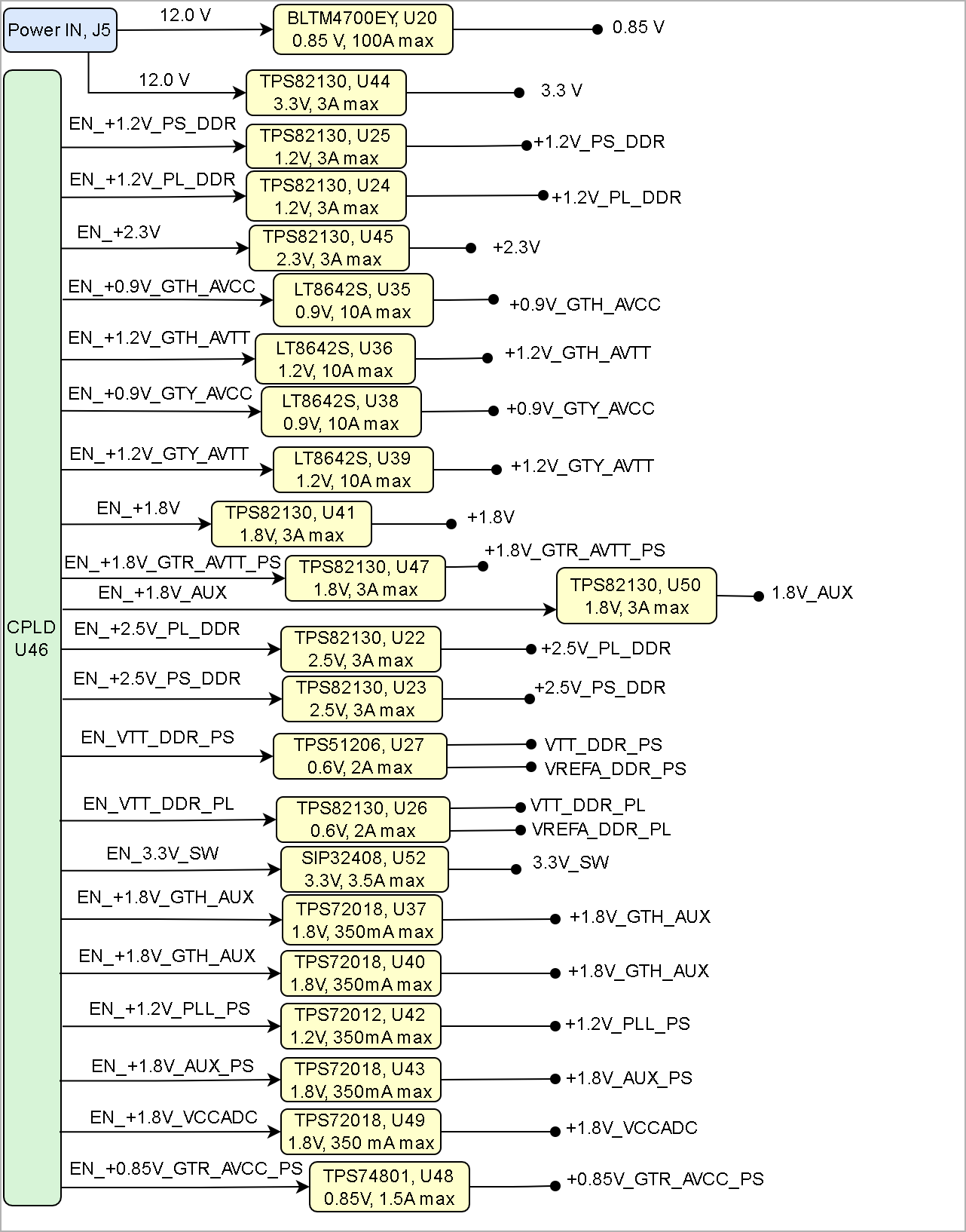
In 'Power and Power-on Sequence' section there are three important digrams which must be drawn: - Power on-sequence
- Power distribution
- Voltage monitoring circuit
|
Power Supply
Power supply with minimum current capability of 3.0 A for system startup is recommended.
Power Consumption
| Scroll Title |
|---|
| anchor | Table_PWR_PC |
|---|
| title | Power Consumption |
|---|
|
| Scroll Table Layout |
|---|
| orientation | portrait |
|---|
| sortDirection | ASC |
|---|
| repeatTableHeaders | default |
|---|
| style | |
|---|
| widths | |
|---|
| sortByColumn | 1 |
|---|
| sortEnabled | false |
|---|
| cellHighlighting | true |
|---|
|
| Power Input Pin | Typical Current |
|---|
| VIN | TBD* |
|
* TBD - To Be Determined
Power Distribution Dependencies
| Scroll Title |
|---|
| anchor | Figure_PWR_PD |
|---|
| title | Power Distribution |
|---|
|
| Scroll Ignore |
|---|
| draw.io Diagram |
|---|
| border | false |
|---|
| |
|---|
| diagramName | TE0865_PWR_PD |
|---|
| simpleViewer | false |
|---|
| width | |
|---|
| links | auto |
|---|
| tbstyle | hidden |
|---|
| diagramDisplayName | |
|---|
| lbox | true |
|---|
| diagramWidth | 641 |
|---|
| revision | 11 |
|---|
|
|
| Scroll Only |
|---|
|
|
Power-On Sequence
| Scroll Title |
|---|
| anchor | Figure_PWR_PS |
|---|
| title | Power Sequency |
|---|
|
| Scroll Ignore |
|---|
| draw.io Diagram |
|---|
| border | false |
|---|
| |
|---|
| diagramName | TE0865_PWR_PS |
|---|
| simpleViewer | false |
|---|
| width | |
|---|
| links | auto |
|---|
| tbstyle | hidden |
|---|
| diagramDisplayName | |
|---|
| lbox | true |
|---|
| diagramWidth | 641 |
|---|
| revision | 4 |
|---|
|
|
| Scroll Only |
|---|
|
|
Voltage Monitor Circuit
The LTM4700 (U20) is a dual 50A or single 100A step-down µModule(power module) DC/DC regulator featuring remote configurability and telemetry-monitoring of power management parameters over standard I2C-based digital interface protocol.
| Scroll Title |
|---|
| anchor | Figure_PWR_VMC |
|---|
| title | Voltage Monitor Circuit |
|---|
|
| Scroll Ignore |
|---|
| draw.io Diagram |
|---|
| border | false |
|---|
| |
|---|
| diagramName | TE0865_PWR_VMC |
|---|
| simpleViewer | false |
|---|
| width | |
|---|
| links | auto |
|---|
| tbstyle | hidden |
|---|
| diagramDisplayName | |
|---|
| lbox | true |
|---|
| diagramWidth | 641 |
|---|
| revision | 4 |
|---|
|
|
| Scroll Only |
|---|
|
|
Power Rails
| Scroll Title |
|---|
| anchor | Table_PWR_PR |
|---|
| title | Module power rails. |
|---|
|
| Scroll Table Layout |
|---|
| orientation | portrait |
|---|
| sortDirection | ASC |
|---|
| repeatTableHeaders | default |
|---|
| style | |
|---|
| widths | |
|---|
| sortByColumn | 1 |
|---|
| sortEnabled | false |
|---|
| cellHighlighting | true |
|---|
|
| Power Rail Name | B2B J1 Pin | B2B J2 Pin | B2B J3 Pin | B2B J4 Pin | Direction | Notes |
|---|
| VCCIO_67 | D10 | - | - | - | In |
| | VCCIO_66 | D20 | - | - | - | In |
| | VCCIO_64 | D35 | - | - | - | In |
| VCCIO_65 | D45 | - | - | - | In |
| | VCCIO_91 | - | A6, | - | - | In |
| | VCCIO_90 | - | B10 | - | - | In |
| | VCCIO_89 | - | A21 | - | - | In |
| | V_IO_CFG | - | A45 | - | - | In |
| | +1.2V_PL_DDR | - | B44 | - | - | Out |
| | VCCIO_68 | - | C29 | - | - | In |
| | VCCIO_88 | - | D44 | - | - | In |
| | +3.3V | - | D60 | - | - | Out |
| | +1.8V | - |
| D60 | - | Out |
|
|
Bank Voltages
| Scroll Title |
|---|
| anchor | Table_PWR_BV |
|---|
| title | Zynq SoC bank voltages. |
|---|
|
| Scroll Table Layout |
|---|
| orientation | portrait |
|---|
| sortDirection | ASC |
|---|
| repeatTableHeaders | default |
|---|
| style | |
|---|
| widths | |
|---|
| sortByColumn | 1 |
|---|
| sortEnabled | false |
|---|
| cellHighlighting | true |
|---|
|
| Schematic Name | | Notes |
|---|
| 64 HP | VCCIO_64 | max 1.8 V |
| | 65 HP | VCCIO_65 | max 1.8 V |
| | 66 HP | VCCIO_66 | max 1.8 V |
| | 67 HP | VCCIO_67 | max 1.8 V |
| | 68 HP | VCCIO_68 | max 1.8 V |
| | 69 HP | VCCIO_69 | 1.2 V |
| | 70 HP | VCCIO_70 | 1.2 V |
| | 71 HP | VCCIO_71 | 1.2 V |
| | 88 HD | VCCIO_88 | max 3.3V | ZU17 Bank 90 HD | | 89 HD | VCCIO_88 | max 3.3 V | ZU17 Bank 91 HD | | 90 HD | VCCIO_88 | max 3.3V | ZU17 Bank 93 HD | | 91 HD | VCCIO_88 | max 3.3V | ZU17 Bank 94 HD | | 128 GTY | MGTAVCC_L | 0.9 V |
| | 129 GTY | MGTAVCC_L | 0.9 V |
| | 224 GTH | MGTAVCC_RS | 0.9 V |
| | 225 GTH | MGTAVCC_RS | 0.9 V |
| | 228 GTH | MGTAVCC_RN | 0.9 V |
| | 229 GTH | MGTAVCC_RN | 0.9 V |
| | 500 PSMIO | VCCO_PSIO0_500 | 1.8 V |
| | 501 PSMIO | VCCO_PSIO0_501 | max 3.3 V |
| | 502 PSMIO | VCCO_PSIO0_502 | 1.8 V |
| | 504 PSDDR | VCCO_PSDDR_504 | 1.2 V |
| | 505 PSGTR | PS_MGTRAVCC | 0.85 V |
|
|
Board to Board Connectors
| Page properties |
|---|
|
- This section is optional and only for modules.
use "include page" macro and link to the general B2B connector page of the module series, For example: 6 x 6 SoM LSHM B2B Connectors
| Include Page |
|---|
| 6 x 6 SoM LSHM B2B Connectors |
|---|
| 6 x 6 SoM LSHM B2B Connectors |
|---|
|
|
| Include Page |
|---|
| 7.5 x 10 ADM6/ADF6 B2B Connectors |
|---|
| 7.5 x 10 ADM6/ADF6 B2B Connectors |
|---|
|
Technical Specifications
Absolute Maximum Ratings
| Scroll Title |
|---|
| anchor | Table_TS_AMR |
|---|
| title | PS absolute maximum ratings |
|---|
|
| Scroll Table Layout |
|---|
| orientation | portrait |
|---|
| sortDirection | ASC |
|---|
| repeatTableHeaders | default |
|---|
| style | |
|---|
| widths | |
|---|
| sortByColumn | 1 |
|---|
| sortEnabled | false |
|---|
| cellHighlighting | true |
|---|
|
| Symbols | Description | Min | Max | Unit | Note |
|---|
| VCCR | Input Supply Voltage | 5.75 | 16 | V | B2B, J5 | | V_IO_CFG | Config Voltage | -0.5 | 3.4 | V | B2B,J3 | | VCCIO_64 | Bank 64 Supply Voltage | -0.5 | 2 | V | B2B,J1 | | VCCIO_65 | Bank 65 Supply Voltage | -0.5 | 2 | V | B2B,J1 | | VCCIO_66 | Bank 66 Supply Voltage | -0.5 | 2 | V | B2B,J1 | | VCCIO_67 | Bank 67 Supply Voltage | -0.5 | 2 | V | B2B,J1 | | VCCIO_68 | Bank 68 Supply Voltage | -0.5 | 2 | V | B2B,J2 | | T_STG | Storage Temperature | -40 | 85 | °C |
|
|
Recommended Operating Conditions
Operating temperature range depends also on customer design and cooling solution. Please contact us for options.
| Scroll Title |
|---|
| anchor | Table_TS_ROC |
|---|
| title | Recommended operating conditions. |
|---|
|
| Scroll Table Layout |
|---|
| orientation | portrait |
|---|
| sortDirection | ASC |
|---|
| repeatTableHeaders | default |
|---|
| style | |
|---|
| widths | |
|---|
| sortByColumn | 1 |
|---|
| sortEnabled | false |
|---|
| cellHighlighting | true |
|---|
|
| Parameter | Min | Max | Units | Reference Document |
|---|
| VCCR | 11.5 | 12.5 | V | See LTM4700 (U20) datasheet. | | V_IO_CFG | 1.14 | 3.4 | V |
| | VCCIO_64 | 0.95 | 1.9 | V |
| | VCCIO_65 | 0.95 | 1.9 | V |
| | VCCIO_66 | 0.95 | 1.9 | V |
| | VCCIO_67 | 0.95 | 1.9 | V |
| | VCCIO_68 | 0.95 | 1.9 | V |
| | T_OPT | 0 | 85 | °C | See components datasheet |
|
Components are mainly classified in 3 temperature groups, according to range specifications: commercial: 0°C - 75°C extended: 0°C - 85°C industrial: -40°C - 85°C
Classification of the module can be locked up here: Article Number Information i.e.: TE0803-03-5D"I"21-AS (The I indicates industrial)
The actual operation temperature range depends on the FPGA/SoC design/utilization and cooling, as well as other variables. Please note: These are only indications!
Physical Dimensions
PCB thickness: 2 mm.
| Scroll Title |
|---|
| anchor | Figure_TS_PD |
|---|
| title | Physical Dimension |
|---|
|
| Scroll Ignore |
|---|
| draw.io Diagram |
|---|
| border | false |
|---|
| |
|---|
| diagramName | TE0865_TS_PD |
|---|
| simpleViewer | false |
|---|
| width | |
|---|
| links | auto |
|---|
| tbstyle | hidden |
|---|
| diagramDisplayName | |
|---|
| lbox | true |
|---|
| diagramWidth | 641 |
|---|
| revision | 2 |
|---|
|
|
| Scroll Only |
|---|
| scroll-pdf | true |
|---|
| scroll-office | true |
|---|
| scroll-chm | true |
|---|
| scroll-docbook | true |
|---|
| scroll-eclipsehelp | true |
|---|
| scroll-epub | true |
|---|
| scroll-html | true |
|---|
| 
|
|
Currently Offered Variants
| Scroll Title |
|---|
| anchor | Table_VCP_SO |
|---|
| title | Trenz Electronic Shop Overview |
|---|
|
| Scroll Table Layout |
|---|
| orientation | portrait |
|---|
| sortDirection | ASC |
|---|
| repeatTableHeaders | default |
|---|
| style | |
|---|
| widths | |
|---|
| sortByColumn | 1 |
|---|
| sortEnabled | false |
|---|
| cellHighlighting | true |
|---|
|
|
Revision History
Hardware Revision History
| Scroll Title |
|---|
| anchor | Figure_RV_HRN |
|---|
| title | Board hardware revision number. |
|---|
|
| Scroll Ignore |
|---|
| draw.io Diagram |
|---|
| border | false |
|---|
| |
|---|
| diagramName | TE0865_RV_HRN |
|---|
| simpleViewer | false |
|---|
| width | |
|---|
| links | auto |
|---|
| tbstyle | hidden |
|---|
| diagramDisplayName | |
|---|
| lbox | true |
|---|
| diagramWidth | 136 |
|---|
| revision | 3 |
|---|
|
|
| Scroll Only |
|---|
|
|
| Scroll Title |
|---|
| anchor | Table_RH_HRH |
|---|
| title | Hardware Revision History |
|---|
|
| Scroll Table Layout |
|---|
| orientation | portrait |
|---|
| sortDirection | ASC |
|---|
| repeatTableHeaders | default |
|---|
| style | |
|---|
| widths | |
|---|
| sortByColumn | 1 |
|---|
| sortEnabled | false |
|---|
| cellHighlighting | true |
|---|
|
| Date | Revision | Changes | Documentation Link |
|---|
| 2021-04-15 | REV01 | Initial Release | REV01 | | 2021-10-21 | REV02 | - Improved PCB trace to simplify production with increased reliability
- All pull down resistors on DCDC enable inputs changed to 1K
| REV02 |
|
Hardware revision number can be found on the PCB board together with the module model number separated by the dash.
Document Change History
| Page properties |
|---|
|
- Note this list must be only updated, if the document is online on public doc!
- It's semi automatically, so do following
Add new row below first Copy "Page Information Macro(date)" Macro-Preview, Metadata Version number, Author Name and description to the empty row. Important Revision number must be the same as the Wiki document revision number Update Metadata = "Page Information Macro (current-version)" Preview+1 and add Author and change description. --> this point is will be deleted on newer pdf export template - Metadata is only used of compatibility of older exports
|
| Scroll Title |
|---|
| anchor | Table_RH_DCH |
|---|
| title | Document change history. |
|---|
|
| Scroll Table Layout |
|---|
| orientation | portrait |
|---|
| sortDirection | ASC |
|---|
| repeatTableHeaders | default |
|---|
| style | |
|---|
| widths | |
|---|
| sortByColumn | 1 |
|---|
| sortEnabled | false |
|---|
| cellHighlighting | true |
|---|
|
| Date | Revision | Contributor | Description |
|---|
| Page info |
|---|
| infoType | Modified date |
|---|
| dateFormat | yyyy-MM-dd |
|---|
| type | Flat |
|---|
|
| | Page info |
|---|
| infoType | Current version |
|---|
| prefix | v. |
|---|
| type | Flat |
|---|
| showVersions | false |
|---|
|
| | Page info |
|---|
| infoType | Modified by |
|---|
| type | Flat |
|---|
| showVersions | false |
|---|
|
| | | 2024-02-07 | | | - Correction Maximum DDR Speed on Key features according AMD Datasheet (still depends assembled ZynqMP)
|
2023-10-24
| | | - Correction Overview Picture GTH B2B connection
| 2023-07-05
| | | - Updated table "CPLD Pin Connections": added signals EN_SOM and PG_SOM; SC_EXT_1 and SC_EXT_4 removed.
- Updated table "Controller signals": PG_VCCINT and EN_VCCINT replaced by PG_SOM and EN_SOM. Description updated respectivelly
- Block diagram updated: added PG_SOM and EN_SOM; SC_EXT_1 and SC_EXT_4 removed.
| | 2022-10-17 | v.67 | JH
| | | 2022-05-30 | v.66 | ED | - Update to the latest version
| -- | all | | Page info |
|---|
| infoType | Modified users |
|---|
| type | Flat |
|---|
| showVersions | false |
|---|
|
| |
|
Disclaimer
| Include Page |
|---|
| IN:Legal Notices |
|---|
| IN:Legal Notices |
|---|
|