Page History
Overview
This guide shows the main components of the TE0802 module and introduces the first steps to get the provided reference design up and running.
This module TE00802 has a Xilinx Zynq Ultrascale+ and several hardware features onboard that allows you to create digital hardware and software designs. For communication and configuration the module board offers a JTAG/UART Interface.
| Scroll Title | |||||||||||||||||||||||||||||||||||||||||||
|---|---|---|---|---|---|---|---|---|---|---|---|---|---|---|---|---|---|---|---|---|---|---|---|---|---|---|---|---|---|---|---|---|---|---|---|---|---|---|---|---|---|---|---|
| |||||||||||||||||||||||||||||||||||||||||||
|
Figure 1: Module TE0802
1 Overview
This guide shows the main components of the TE0802 module and introduces the available script-based reference design to get the board up and running.
|
Prerequisites
| Hardware | Software |
|---|
- TE00802 module
- Micro-USB cable
- Vitis (Vivado included)
- PuTTY (or any other serial communicator)
- TE0802 Reference Design
1.2 Getting Started with the TE0802
The module TE00802 has a Xilinx Spartan-7 FPGA onboard that allows you to create extensive digital hardware and software designs.
Most of the FPGA IOs are spread around the carrier. The TE0717 is assembled with HyperRAM (64 Mbit), QSPI non-volatile Flash memory (64 Mbit) and plenty of IOs which enable great hardware expandability. For communication and configuration the module board offers a JTAG/UART Interface.
This Getting Started Guide shows how to set up the board, attach the jumpers, wire it up and connect it with the software. The TE0802 Test Board description goes into "how to use the provided reference design" and in here we touch the aspect of how to add your own IP to the design. This includes changing the Vivado Block Design, regenerating the bitstream and using the hardware export(.xsa file) in Vitis to develop software that runs on the MicroBlaze.
| Page properties | ||||
|---|---|---|---|---|
| ||||
Old text: The module TE0717 has a Xilinx Spartan-7 FPGA onboard that allows you to create extensive digital hardware and software designs. Most of the FPGA IOs are spread arround the carrier. The TE0717 is assembled with HyperRAM(64 Mbit), QSPI non-volatile Flash memory(64 Mbit) and plenty of IOs which enable great hardware expandability. For communication and configuration the carrier offers a JTAG/UART Interface. This Getting Started Guide shows how to set up the board, attach the jumpers, wire it up and connect it with the software. Over the course of this guide we will go into "how to use the provided reference design" and touch several aspects of "how to modify the design according to your needs". This includes changing the Vivado Block Design, regenerating the bitstream and using the hardware export(.xsa file) in Vitis to develop software that runs on the MicroBlaze. Here we will not build the whole project from scratch since that would go beyond the scope of this guide. |
|
|
Documentation
- Official links to the shop:
- Technical Reference Manual:
- Resources & Reference Designs:
Hardware Features and Overview
| Expand | ||
|---|---|---|
|
| ||||||||||||||||||||||||
| ||||||||||||||||||||||||
| Scroll Title | |||||||||||||||||||||||
|---|---|---|---|---|---|---|---|---|---|---|---|---|---|---|---|---|---|---|---|---|---|---|---|
| |||||||||||||||||||||||
|
Firgure 2: TE0717+TEB0717 Hardware Blockdiagram
Basic IOs<->FPGA connections are as following, Table 1:
FPGA Pin
| Info |
|---|
Information on IO routing and FPGA pin connections can be found in the |
Reference Design - Introduction
| Scroll Ignore | ||||||||||||||
|---|---|---|---|---|---|---|---|---|---|---|---|---|---|---|
| ||||||||||||||
| Page properties | ||||
|---|---|---|---|---|
| ||||
ACHTUNG!!! Hier soll noch entschieden werden, ob hier nur kurz auf das Referenzdesign eingegangen wird und die Inhalte im public doc - test board Beschreibung rein genommen werden bzw ... was hier überhaupt noch sinnvoll reingehört ? |
The provided reference design "TE0802 test board" we are introducing in this Getting started guide interacts with most of the peripheral on the module. It shows as an example how to connect the different parts of the module to simplify the development of your own application. You can use it for your own design but keep in mind the overall FPGA resources and power consumption before deployment. The most important steps to get it up and running from the scratch are explained on TE0802 Test Board. The Download is available here.
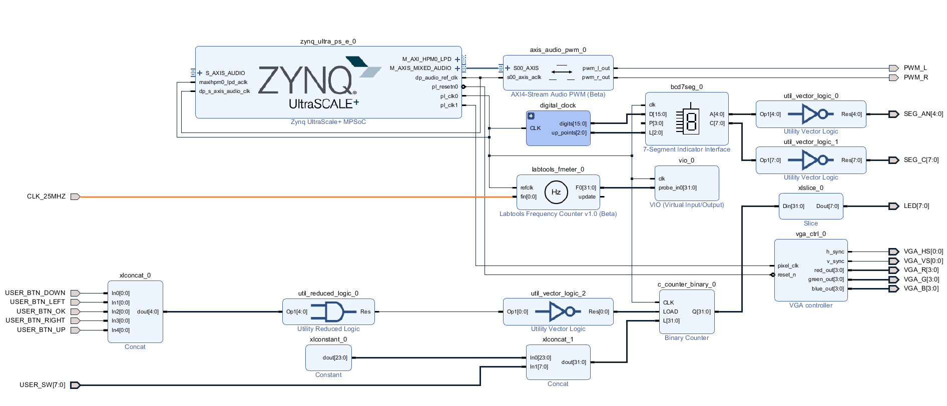
An overview of the components used in this reference design is illustrated in the following figure:
| Scroll Title | ||||||
|---|---|---|---|---|---|---|
| ||||||
 |
Hardware Setup and Power up in QSPI-Boot mode
| Scroll Ignore | ||||||||||||||
|---|---|---|---|---|---|---|---|---|---|---|---|---|---|---|
| ||||||||||||||
Preparations
- Download the source code and configuration files for "TE0802 test_board" reference design. Ensure that your download files match your Vivado version.
Check the settings from DIP-Switch S1 (JTAG):
S1.1 S1.2 S1.3 S1.4 OFF OFF OFF OFF Run _create_win_setup.cmd/_create_linux_setup.sh and follow instructions on shell:
Code Block language bash theme Midnight title _create_win_setup.cmd/_create_linux_setup.sh ------------------------Set design paths---------------------------- -- Run Design with: _create_win_setup -- Use Design Path: <absolute project path> -------------------------------------------------------------------- -------------------------TE Reference Design--------------------------- -------------------------------------------------------------------- -- (0) Module selection guide, project creation...prebuilt export... -- (1) Create minimum setup of CMD-Files and exit Batch -- (2) Create maximum setup of CMD-Files and exit Batch -- (3) (internal only) Dev -- (4) (internal only) Prod -- (c) Go to CMD-File Generation (Manual setup) -- (d) Go to Documentation (Web Documentation) -- (g) Install Board Files from Xilinx Board Store (beta) -- (a) Start design with unsupported Vivado Version (beta) -- (x) Exit Batch (nothing is done!) ---- Select (ex.:'0' for module selection guide):- Press '0' and enter to start "Module Selection Guide"
- Select your assembly version
- validate selection
- press '2' and enter to "create Vivado project" and "create and open delivery binary folder"
- Depending on the preferred application, continue with chapter "Linux in QSPI-Boot mode" or "'Hello Trenz' in QSPI-Boot mode"
Linux in QSPI-Boot mode
- Connect the MicroUSB cable from your module board with your PC
- Connect peripherals to devices
- VGA, display port → monitor
- USB → keyboard
- ...
- Connect the module board with the power supply (5V)
- Power on module board
Program 'u-boot' application on QSPI flash
Code Block language bash theme Midnight title run on Vivado TCL (Script programs BOOT.bin on QSPI flash) TE::pr_program_flash -swapp u-boot- Power off module board
- Copy image.ub, init.sh and boot.scr on SD card (e.g. <project folder>\test_board\_binaries_TE0802-02-2AEV2-A\boot_linux)
Switch the DIP-Switch S1 to QSPI-Boot mode
S1.1 S1.2 S1.3 S1.4 ON OFF OFF OFF - Insert the SD card into the module board
Power on the module board
In case the QSPI Flash is loaded with the reference design, you can connect to the board with a program like PuTTY. Just open up a serial session with baudrate of 115200 and the right COM port (visible in Device Manager).
| Info |
|---|
Information on IO routing and FPGA pin connections can be found in the schematics. |
2 Board Power-Up
2.1 TE0802 Hardware Setup and Power up
Check the Jumper setting
Scroll Title anchor Figure_VHM title-alignment center 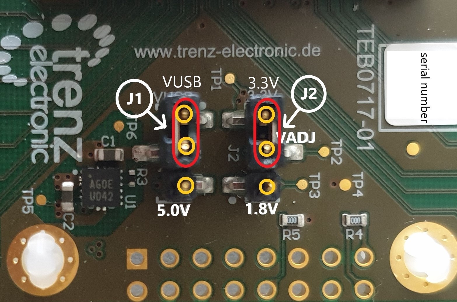
Figure 3: Jumper setting
The Voltage set with Jumper J1 determines the source of the input voltage for the voltages regulator chip U1 to the left of J1. Either 5V from the MicroUSB port(VUSB) or 5V from pin header J4.
With the shown setting of Jumper J2 the voltage VADJ is set to 3.3V that comes from the carriers voltage regulator chip U1. The 1.8V comes from the module. The Voltage VADJ is wired to the module and is used as the BANK34 supply voltage.
- Use a MicroUSB cable to connect your board to the PC.cc
title Terminal example 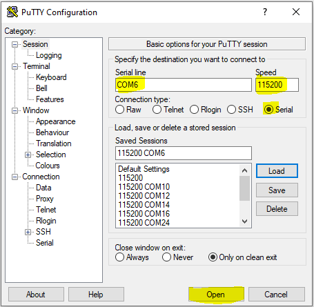
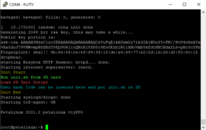
Boot process
Zynq Boot ROM loads FSBL from QSPI into OCM,
- FSBL init PS, programs PL using the bitstream and loads U-boot from QSPI into DDR,
- U-boot loads Linux (image.ub) from SD into DDR
- For usage instructions please refer to chapter Linux application
'Hello Trenz' in QSPI-Boot mode
- Connect the MicroUSB cable from your module board with your PC
Connect the module board with the power supply (5V)
Power on module board
Program 'hello_te0802' application on QSPI flash
Code Block language bash theme Midnight title run on Vivado TCL (Script programs BOOT.bin on QSPI flash) TE::pr_program_flash -swapp hello_te0802Switch the DIP-Switch S1 to QSPI-Boot mode:
S1.1 S1.2 S1.3 S1.4 ON OFF OFF OFF Restart the module boardAll the LEDs are simply routed to the FPGA, hence none of them should be turned on. If the qspi flash on the module is preloaded with a design though, it might be that some LEDs are blinking.
In case the QSPI Flash is loaded with the reference design, you can connect to the board with a program like PuTTY. Just open up a serial session with baud-rate baudrate of 9600 115200 and the right COM-port (visible in Device Manager).
You may need to press the RESET-button.Scroll Title anchor Figure_VHM title-alignment center 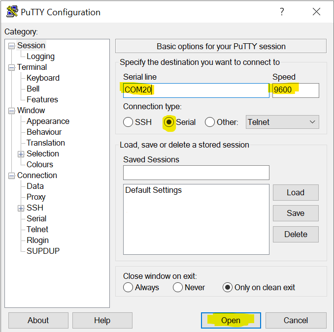
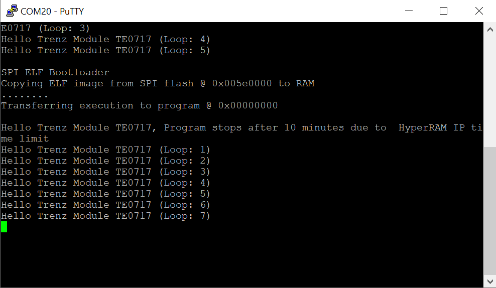
title Figure 4: Terminal(MicroBlaze output)
2.2 Reference Design - Introduction
| Page properties | ||||
|---|---|---|---|---|
| ||||
ACHTUNG!!! Hier soll noch entschieden werden, ob hier nur kurz auf das Referenzdesign eingegangen wird und die Inhalte im public doc - test board Beschreibung reingenommen werden bzw ... was hier überhaupt noch sinnvoll reingehört ? |
We provide a reference design that interacts with most of the peripheral on the module. The provided design "TE0717 test board" shows how to connect the different parts of the module to simplify the development of your own application. You can use it for your own design but keep in mind the overall FPGA resources and power consumption before deployment.
The reference design we are introducing in this guide is "TE0717 test board". The most important steps to get it up and running are explained on TE0717 Test Board. The Download is available here.
The reference design is only usable with the specified Vivado/Vitis version. Always use the same version of Xilinx Software for one Project. (e.g. use reference design 2021.2 with vitis installation 2021.2)
The components of the reference design are illustrated in the following figure:Terminal example 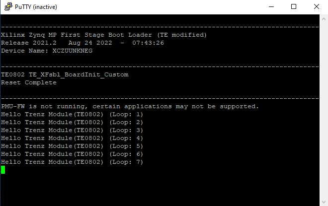
Hardware Setup and Power up in SD-Boot mode
| Scroll Ignore | ||||||||||||||
|---|---|---|---|---|---|---|---|---|---|---|---|---|---|---|
| ||||||||||||||
Linux in SD-Boot mode
- Download the source code and configuration files for "TE0802 test_board" reference design. Ensure that your download files match your Vivado version.
Run _create_win_setup.cmd/_create_linux_setup.sh and follow instructions on shell:
Code Block language bash theme Midnight title _create_win_setup.cmd/_create_linux_setup.sh ------------------------Set design paths---------------------------- -- Run Design with: _create_win_setup -- Use Design Path: <absolute project path> -------------------------------------------------------------------- -------------------------TE Reference Design--------------------------- -------------------------------------------------------------------- -- (0) Module selection guide, project creation...prebuilt export... -- (1) Create minimum setup of CMD-Files and exit Batch -- (2) Create maximum setup of CMD-Files and exit Batch -- (3) (internal only) Dev -- (4) (internal only) Prod -- (c) Go to CMD-File Generation (Manual setup) -- (d) Go to Documentation (Web Documentation) -- (g) Install Board Files from Xilinx Board Store (beta) -- (a) Start design with unsupported Vivado Version (beta) -- (x) Exit Batch (nothing is done!) ---- Select (ex.:'0' for module selection guide):- Press '0' and enter to start "Module Selection Guide"
- Select your assembly version
- validate selection
- press '1' and enter to "create and open delivery binary folder"
- Connect the MicroUSB cable from your module board with your PC
- Connect peripherals to devices
- VGA, display port → monitor
- USB → keyboard
- ...
- Connect the module board with the power supply (5V)
- Copy BOOT.bin, image.ub, init.sh and boot.scr on SD card (e.g. <project folder>\test_board\_binaries_TE0802-02-2AEV2-A\boot_linux)
Switch the DIP-Switch S1 to SD-Boot mode
S1.1 S1.2 S1.3 S1.4 ON ON OFF OFF - Insert the SD card into the module board
Power on the module board
You can connect to the board with a program like PuTTY. Just open up a serial session with baudrate of 115200 and the right COM port (visible in Device Manager).
Scroll Title anchor Figure_VHM title-alignment center
Figure 5: Blockdiagram of the Reference Design
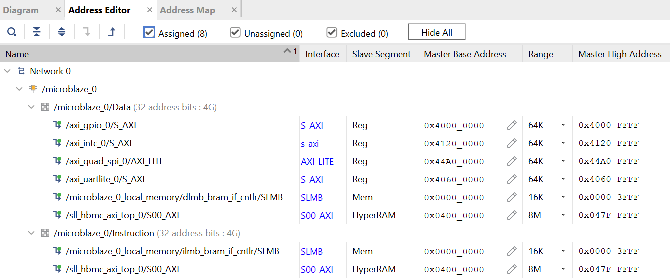
The Cores are connected via the AXI Interface with the MicroBlaze Processor. How they are mapped into the address space can be seen in the address editor:title Terminal example Boot process
Zynq Boot ROM loads FSBL from SD into OCM,
- FSBL init PS, programs PL using the bitstream and loads U-boot from SD into DDR,
- U-boot loads Linux (image.ub) from SD into DDR
- For usage instructions please refer to chapter Linux application
Linux Application
| Scroll Ignore | ||||||||||||||
|---|---|---|---|---|---|---|---|---|---|---|---|---|---|---|
| ||||||||||||||
After the Linux boot is complete, you can use the Linux shell and the connected peripherals
I2C
| Code Block | ||||||
|---|---|---|---|---|---|---|
| ||||||
i2cdetect -l        (Shows a list of the available I2C buses)
i2cdetect -y -r 1 (check I2C 1 Bus) |
Real Time Clock (RTC)
| Code Block | ||||||
|---|---|---|---|---|---|---|
| ||||||
dmesg | grep rtc    (RTC check)
hwclock --test |
Ethernet
| Code Block | ||||||
|---|---|---|---|---|---|---|
| ||||||
udhcpc              (ETH0 check)
ifconfig (shows the configuration of the network interface) |
USB
| Code Block | ||||||
|---|---|---|---|---|---|---|
| ||||||
lsusb (USB check) |
PCIe (M.2 SSD)
| Code Block | ||||||
|---|---|---|---|---|---|---|
| ||||||
lspci (PCIe check) |
Audio
| Code Block | ||||||
|---|---|---|---|---|---|---|
| ||||||
aplay /<link to mounted sd card>/<filename>.wav (e.g. aplay /run/mount/sd/<filename>.wav) |
| Info |
|---|
|
VGA
- connect VGA to monitor and adjust source (it shows test pattern)
Display Port
- second linux console output will be shown on the monitor, when boot process is finished.
- connect keyboard to TE0802 USB, to interact with the second console
- petalinux login: root
- password: root
Webserver
Expand title insert IP on web browser to start web interface 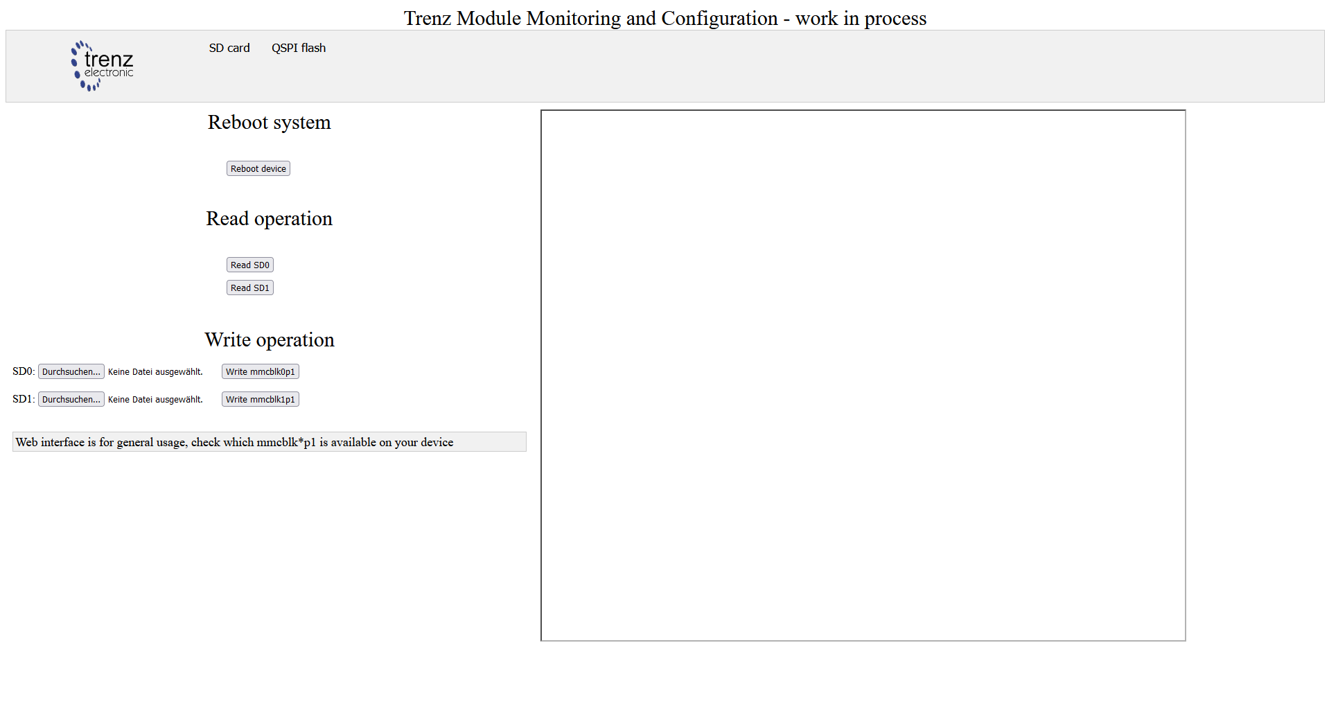
Startup Script
- If there is a start script named 'init.sh' on the SD card, it is loaded and executed shortly before the Linux boot process is completed.
- User bash code can be inserted on 'init.sh'
Monitoring input clock (25MHz)
- Open Vivado HW-Manager and add VIO signal to dashboard (*.ltx located on prebuilt folder)
changed Value from 25MHz CLK to unsigned. Note: Frequency Counter is inaccurate and displayed unit is Hz
Scroll Title anchor Figure_VHM title-alignment center
title
Figure 6: Vivado Address Editor - Address Mapping
For example the AXI GPIO IP Core which has a LED1 connected to it, can be controlled with software(C/C++) by raising the bits mapped to the address 0x4000 0000.
The VIO Core enables you to control connected IOs via the Vivado Hardware Manager(like LED2).
Vivado Hardware Manager 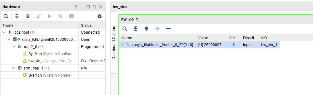
userLEDs
- The user LEDs indicate a binary counter, which is reset by pressing one of the cross buttons
7-Segment LCD Display
- LCD is connected to counter
DIP-Switch
- Determines the reset start value from the binary counter of userLEDs
Notes
Document Revision History
| Expand | |||||||||||||||||||||||||||||||||||||||||||||||||||||||||||||||||||||
|---|---|---|---|---|---|---|---|---|---|---|---|---|---|---|---|---|---|---|---|---|---|---|---|---|---|---|---|---|---|---|---|---|---|---|---|---|---|---|---|---|---|---|---|---|---|---|---|---|---|---|---|---|---|---|---|---|---|---|---|---|---|---|---|---|---|---|---|---|---|
| |||||||||||||||||||||||||||||||||||||||||||||||||||||||||||||||||||||
|
| Scroll Only | ||
|---|---|---|
|
| Scroll pdf ignore | ||||||
|---|---|---|---|---|---|---|
|
Overview
Content Tools