Page History
...
- Some Programmable Device: MCU, CPU, CPLD, FPGA, SoC
- Working Programming or Configuration interface or means to boot the Programmable Device
- Timing Source (Clock), can be external or internal, must be be enabled
- Active Power to all required power domains of the Programmable Device
- Release of main Reset
- LED Connected to some user controllable I/O Port of the Programmable Device
- LED must be assembled with right polarity and proper current limiting resistor
- Valid I/O Voltage applied to the I/O Bank with the user LED
| Warning |
|---|
| If any of those requirements are missing |
...
| you may encounter problems with LED Blinky. |
Programmable Device
Timing Source
...
If we do not know how to access the time/clock source or if we are not sure if the clock is enabled and running we have an potential problem and we can not proceed to the LED Blinky unless we have identified an active/enabled accessible clock source we can use for timing.
FPGA Devices
GT Clock
Gigabit Transceiver Clock may also be used as FPGA Fabric clock.
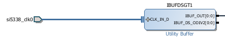
Clock buffers for GT Clock in Xilinx 7 Series Devices (example from TE0745 design)
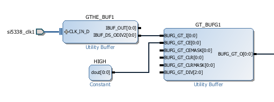
Clock buffers for GT Clock in Ultrascale Devices (example from TE0841 design)
ZYNQ Devices
In Zynq System the main System Clock is connected PS (Processing Subsystem) and is not directly available to the PL (Programmable Logic - FPGA) unless the PS has enabled it during FSBL boot process. So if we have a generic Zynq Board then we can not expect to have clocks available to the FPGA until the Processing system has provided them. There may be clocks available to the PL that are active when the PS is not booted but this not a requirement.
If our goal is to make a LED to blink (from PL in Zynq Device), then the safest way is to use FPGA Configuration Master Clock this clock is always available and accessible in the same way, we do not need to know any specifics to the board we have and we do not depend on PS init done by FSBL.
ZYNQ MPSoC Devices
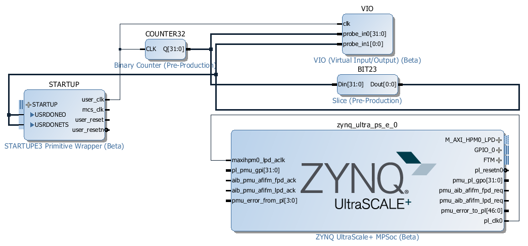
This design blinks a LED connected to DONE pin and also a VIO Pin, on any Zynq MPSoC device, without using any clocks provided by the externally, and without the use of PS supplied clocks. LED Toggle rate is about 2 Hz.
Valid I/O Voltage
It is very common that modern Integrated Circuits have separate power supply pins for I/O Voltage. That voltage if applied control the output levels from the device, if the Voltage is too low or missing then it is not possible to have enough current from the device I/O Pin to make a LED Lit.
FPGA and SoC SoM's can have fixed and user controlled Voltages for the I/O Banks. It is important to assure that the I/O Bank that controls the LED has a valid Supply Voltage applied.If
| Note |
|---|
| NOTE: Missing VCCIO Voltage will not cause AXI GPIO to freeze, no matter if it is connected to MicroBlaze or Zynq Processing Block. |
| Note |
|---|
| NOTE: Changing I/O Standard will not change the Bank Supply Voltage or enable it. |
you are not sure about the I/O Banks Voltage supplies then there are some options to try.
DONE LED
If there is on board LED directly connected to FPGA "DONE" output, then it is also possible to control it as long as it is possible to configure the FPGA (or PL portion of Zynq). For Zynq the PS subsystem is not needed if configuration is done via JTAG.
...
| MIO LED | DONE LED | User LED PL | Notes | |
|---|---|---|---|---|
| TE0710 | - | |||
| TE0711 | - | |||
| TE0712 | - | No* | Yes* | LED's are routed to PL I/O by System Control CPLD |
| TE0714 | - | No | Yes | One fixed LED on PL,1.8V or 3.3V I/O Voltage always present |
| TE0720 | MIO7 | Yes, Fixed | Yes* | System control CPLD can remap the LED functions during FSBL |
| TE0725 | - | Yes | Yes | LED's power always available |
| TE0729 | MIO7 | Yes | - | |
| TE0741 | - | |||
| TE0745 | MIO | - | ||
| TE0782 | ||||
| TE0841 | - | - | Yes |
...
| Base | User LED's | Notes |
|---|---|---|
| TE0701 | up to 8 max | All LED's controlled by the System Control CPLD, some require user I/O Bank voltage |
| TE0703 | 2* | User supplied I/O Voltage |
| TE0705 | ||
| TE0706 | 0 | Can use RJ45 LED's as PL User LED's |
| TEB0729 |
Blinky Examples
MicroBlaze MCS
TBD
MicroBlaze
TBD
Arduino F32C
F32C is an Open Source Soft Processor and SoC system that has ready to use support for Arduino IDE (using Arduino IDE package manager). More details on installation into Arduino IDE can be found here. F32C project is hosted at github f32c/f32c.
...
There is no need to have any Xilinx tools installed or any toolchain/compiler either.
| SoM | Variant | Clock | RAM KBlinky LED is: | Available | Test Setup | Notes | |
|---|---|---|---|---|---|---|---|
| TE0710 | A35 and larger | 100MHz | 128 | NOW | TE0701 | ||
| TE0711 | A35 and larger | 100MHz | 128 | NOW | TE0701 | ||
| TE0712 | all | 100MHz | 128 | 8 | NOW | TE0701 | |
| TE0713 | all | 100MHz | 128 | ||||
| TE0714 | 100MHz | 128 | NOW | ||||
| TE0720 | soon | ||||||
| TE0722 | 100Mhz | soon | |||||
| TE0723 | soon | ||||||
| TE0725 | A35 and larger | 100MHz | 128 | 8 | NOW | TE0790 | |
| TE0726 | soon | ||||||
| TE0741 | all | 128 | NOW | ||||
| TE0841 | KU35 | 100MHz | 128 | 8 | NOW | TE0703 modified 1.8V |
F32C_demo availability - designs and prebuilt images ready to be used with Arduino IDE.
...
This is Arduino IDE screenshot after downloading LED Blinky sketch to F32C inside FPGA, selected generic FPGA board with 128K RAM and 100MHz Clock. After download the on-board LED on the FPGA/SoC SoM will blink.
Troubleshooting Tips
If you are not sure to what pins the LED(s) are connected it is possible to create a "dummy" FPGA design with "UNUSED PIN PULLUP" option. If FPGA is loaded with bitfile then any LED that is connected in active high configuration will be on, if the I/O Bank is powered. The internal pullup current is sufficient to make most modern LED to be lit (not very bright).
If you know that there are LED's connected to FPGA and they do not get lit with "unused pin pullup" FPGA design, then most likely the I/O Bank with the LED's has no power.
Overview
Content Tools