Page History
...
All parts cover at least industrial temperature range of -40°C to +85°C. The module operating temperature range depends on customer design and cooling solution. Please contact us for options .Contact us and for modified PCB-equipping due increasing cost-performance-ratio and prices for large-scale order.
...
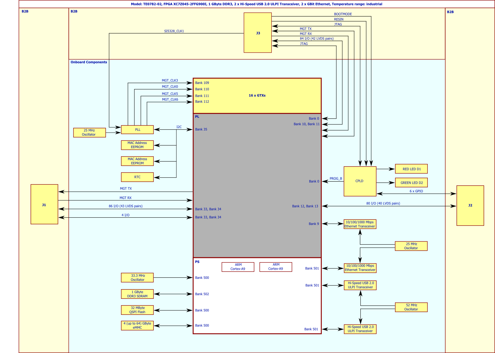
- 2 x Gbps Ethernet PHY transceiver
- 16-Bit wide 2 x 512 MByte DDR3 SDRAM
- 32 MByte QSPI Flash Memory for configuration, operation and to store data
- eMMC (4 GByte in standard configuration)
- 2 x USB PHY transceiver
- 16 GTX high-performance transceiver lanes
- powerful switch-mode power supplies for all on-board voltages
- large number of configurable I/Os is provided via rugged high-speed stacking strips
Block Diagramm
Key Features
- Xilinx Zynq-7 XC7Z035, XC7Z045 or XC7Z100 SoM
- Rugged for shock and high vibration
- Dual ARM Cortex-A9 MPCore
- 1 GByte DDR3 SDRAM (2 x 16-Bit wide 512 MByte DDR3 SDRAM)
- 32 MByte QSPI Flash memory
- 2 x Hi-Speed USB2.0 ULPI transceiver PHY
- 2 x Gigabit (10/100/1000 Mbps) Ethernet transceiver PHY
- 4 GByte eMMC (optional up to 64GByte)
- 2 x MAC-Address EEPROMs
- optional 2 x 8 MByte HyperRAM (max 2 x 32 MByte HyperRAM) or optional 2 x 32 64 MByte HyperFLASH
- Temperature compensated RTC (real-time clock)
- Si5338 PLL for GTX Transceiver clocks
- Plug-on module with 3 x 160-pin high-speed strips
- 16 GTX high-performance transceiver lanes
- GT transceiver clock inputs
- 254 FPGA I/O's (125 LVDS pairs)
- On-board high-efficiency DC-DC converters
- System management
- eFUSE bit-stream encryption
- AES bit-stream encryption
- Evenly-spread supply pins for good signal integrity
- User LED
...
Signals, Interfaces and Pins
System
...
Controller CPLD I/O Pins
Special purpose pins to configure and operate the System Controller CPLD (IC U14) used by TE0782
| Name | Note |
|---|---|
| BOOTMODE | user configurable (CPLD) |
| CONFIGX | user configurable (CPLD) |
| JTAGENB | JTAG operation |
| RESIN | System-reset |
| CLPD_GPIO0 | user GPIO |
| CLPD_GPIO1 | user GPIO |
| CLPD_GPIO2 | user GPIO |
| CLPD_GPIO3 | user GPIO |
| CLPD_GPIO4 | user GPIO |
| CLPD_GPIO5 | user GPIO |
Small CPLD controls some functions of the SoM, this CPLD can be updated by the end user if support is designed on customer base.
Boot Modes
TE0782 supports primary boot from
...
| Note |
|---|
JTAGENB pin in J3 should be kept low or grounded for normal operation. |
Clocking
Silabs Multisynth PLL Si5338 can deliver GT reference clocks to all 4 GT Banks. Additionally a GT Reference clock can be generated on the base board for any of the 4 GT Banks. There is reference clock available on the TE0782 for Si5338, there is no need to supply a master reference clock from the base.
| Clock | Frequency | IC | ZYNQ PS / PL | Notes |
|---|---|---|---|---|
| PS | ||||
| Clock | Frequency | IC | FPGA | Notes |
| PS CLK | 33.3333 MHz | U61 | BANK500, PS_CLK | PS Subsystem main clock |
| 10/100/1000 Mbps ETH PHYs reference | 25 MHz | U11 | - | |
| USB PHY reference | 52 MHz | U7 | - | |
PLL reference | 25 MHz | U3 | - | |
GT REFCLK1 | - | B2B connector | BANK110, Pin AC7/AC8 | Externally supplied from base |
GT REFCLK4 | - | B2B connector | BANK111, Pin U7/U8 | Externally supplied from base |
quad programmable clock (I2C) SI5338A | user | U2- | BANK110, Pin AA8/AA7 BANK109, Pin AF10/AF9 BANK111, Pin W8/W7 BANK112, Pin N8/N7 | GT REFCLK0 GT REFCLK3 GT REFCLK5 GT REFCLK6 |
Processing System (PS) Peripherals
| Peripheral | IC | Designator | ZYNQ PS / PL | MIO | Notes | |
|---|---|---|---|---|---|---|
| QSPI Flash | S25FL256SAGBHI20 | U38 | QSPI0 | MIO1...MIO6 | - | |
| Ethernet0 ETH0 10/100/1000 Mbps PHY | 88E1512-A0-NNP2I000 | U18 | ETH0; GPIO BANK35 | MIO16...MIO27, MIO52, MIO53 | - | |
| Ethernet0 ETH0 10/100/1000 Mbps PHY Reset | GPIO | MIO7 | ETH1_RESET33 (MIO7) -> CPLD -> ETH1_RESET | |||
| Ethernet1 ETH1 10/100/1000 Mbps PHY | 88E1512-A0-NNP2I000 | U20 | GPIO BANK9, BANK35 | - | - | PHY can be used with soft Ethernet MAC IP also |
| ETH1 Ethernet1 10/100/1000 Mbps PHY Reset | GPIO BANK35, Pin B15 | - | - | |||
| USB0 | USB3320C-EZK | U4 | USB0 | MIO28...MIO39 | - | |
| USB0 Reset | GPIO | MIO0 | OTG_RESET33 (MIO0) -> CPLD -> OTG_RESET | |||
| USB1 | USB3320C-EZK | U8 | USB1 | MIO40...MIO51 | - | |
| USB1 Reset | GPIO | MIO0 | OTG_RESET33 (MIO0) -> CPLD -> OTG_RESET | |||
| Clock PLL | Si5338 | U2 | I2C | BANK35, Pin L14/L15 | Low jitter phase locked loop | |
| e-MMC (embedded e-MMC) | MTFC4GMVEA-4M IT | U15 | SDIO0 | MIO10...MIO15 | - | |
| HyperFlash RAM | S26KS512SDPBHI00x | U9 | GPIO BANK35 | - | optional 2 x 8 MByte HyperRAM (max 2 x 32 MByte HyperRAM) or optional 2 x 32 64 MByte HyperFLASH | |
| HyperFlash RAM | S26KS512SDPBHI00x | U12 | GPIO BANK35 | - | as above | |
| EEPROM I2C | 24LC128-I/ST | U26 | GPIO BANK35, Pin L14/L15 | - | - | |
| EEPROM I2C | 24AA025E48T-I/OT | U22 | GPIO BANK35, Pin L14/L15 | - | MAC Address | |
| EEPROM I2C | 24AA025E48T-I/OT | U24 | GPIO BANK35, Pin L14/L15 | - | MAC Address | |
| RTC | ISL12020MIRZ | U17 | GPIO BANK35, Pin L14/L15 | - | Temperature compensated real time clock | |
| RTC Interrupt | ISL12020MIRZ | U17 | - | - | RTC_INT -> CPLD |
...
| MIO | Configured as | B2B | Notes |
|---|---|---|---|
| 0 | OTG-RST33 | - | connected to CPLD |
| 1 | QSPI0 | - | SPI Flash-CS |
| 2 | QSPI0 | - | SPI Flash-DQ0 |
| 3 | QSPI0 | - | SPI Flash-DQ1 |
| 4 | QSPI0 | - | SPI Flash-DQ2 |
| 5 | QSPI0 | - | SPI Flash-DQ3 |
| 6 | QSPI0 | - | SPI Flash-SCK |
| 7 | ETH1_RESET33 | - | connected to CPLD |
| 8 | GPIO | - | connected to CPLD and Pull-Up 3.3V |
| 9 | GPIO | - | connected to CPLD |
| 10 | MMC-D0 | - | - |
| 11 | MMC-CMD | - | - |
| 12 | MMC-CCLK | - | - |
| 13 | MMC-D1 | - | - |
| 14 | MMC-D2 | - | - |
| 15 | MMC-D3 | - | - |
| 16..27 | ETH0 | - | Ethernet RGMII PHY |
| 28..39 | USB0 | - | USB0 ULPI PHY |
| 40...51 | USB1 | - | USB1 ULPI PHY |
| 52 | ETH0 MDC | - | - | 53 | ETH0 MDIO | - | -
| 40...51 | USB1 | - | USB1 ULPI PHY |
| 52 | ETH0 MDC | - | - |
| 53 | ETH0 MDIO | - | - |
Pin Definitions
Pins named _vrn and _vrp are connected to ZYNQ PL HP Bank special purpose pins VRN/VRP. If needed they can be connected to DCI calibration resistors on the base. If not, then those pins can be used as general purpose I/O.
Bank B35 has 100 ohm DCI calibration resistors installed on TE0782, it is also possible to "borrow" the DCI calibration from B35 for banks B34, and B33. For detailed usage of the DCI check Xilinx documentation.
I2C Interface
The on-board I2C components are connected to BANK35, Pin L15 (I2C_SDA) and to BANK35, Pin L14 (I2C_SCL).
...
LED's
D1 - Onboard RED LED
| Frequency of LED-Toggling [1/2.6sec] | Status |
|---|---|
| 1 | Power problem |
| 2 | MGT Power problem |
| 3 | Reset from mainboard |
| 4 | FPGA not programmed |
This function depend on the CPLD revision.
...
ETH1 PHY connection:
| PHY PIN | ZYNQ PS / PL | System Controller CPLD | Notes |
|---|---|---|---|
| MDC/MDIO | MIO52, MIO53 | - | - |
| LED0 | BANK35, Pin B12 | - | - |
| LED1 | BANK35, Pin C12 | - | - |
| Interrupt | BANK35, Pin A15 | - | - |
| CONFIG | BANK35, Pin F14 | - | - |
| RESETn | - | Pin 53 | ETH1_RESET33 (MIO7) -> CPLD -> ETH1_RESET |
| RGMII | MIO16..MIO27 | - | |
| MDI | - | - | on B2B J2 connector |
ETH2 PHY connection:
| PHY PIN | ZYNQ PS / PL | System Controller CPLD | Notes |
|---|---|---|---|
| MDC/MDIO | BANK35, Pin C17/B17 | - | - |
| LED0 | BANK35, Pin K15 | - | - |
| LED1 | BANK35, Pin B16 | - | - |
| Interrupt | BANK35, Pin A17 | - | - |
| CONFIG | BANK35, Pin E15 | - | Pin connected to GND, PHY Address is strapped to 0x00 by default |
| RESETn | BANK35, Pin B15 | - | - |
| RGMII | BANK9 | - | - |
| MDI | - | - | on B2B J2 connector |
...
USB0 PHY connection:
| PHY PinZynq Pin | ZYNQ PS / PL | CPLD | B2B Name (J2) | Notes |
|---|---|---|---|---|
| ULPI | MIO28..39 | - | - | Zynq USB0 MIO pins are connected to the PHY |
| REFCLK | - | - | - | 52MHz from on board oscillator (U7) |
| REFSEL[0..2] | - | - | - | 000 GND, select 52MHz reference Clock |
| RESETB | MIO0 | OTG_RESET33 | - | OTG_RESET33 -> CPLD -> OTG_RESET |
| CLKOUT | MIO36 | - | - | Connected to 1.8V selects reference clock operation mode |
| DP,DM | - | - | USB1_D_P, USB1_D_N | USB Data lines |
| CPEN | - | - | VBUS1_V_EN | External USB power switch active high enable signal |
| VBUS | - | - | USB1_VBUS | Connect to USB VBUS via a series resistor. Check reference schematic |
| ID | - | - | OTG1_ID | For an A-Device connect to ground, for a B-Device left floating |
...
USB1 PHY connection:
| PHY PinZynq Pin | ZYNQ PS / PL | CPLD | B2B Name (J2) | Notes |
|---|---|---|---|---|
| ULPI | MIO40..51 | - | - | Zynq USB1 MIO pins are connected to the PHY |
| REFCLK | - | - | - | 52MHz from on board oscillator (U7) |
| REFSEL[0..2] | - | - | - | 000 GND, select 52MHz reference Clock |
| RESETB | MIO0 | OTG_RESET33 | - | OTG_RESET33 -> CPLD -> OTG_RESET |
| CLKOUT | MIO48 | - | - | Connected to 1.8V selects reference clock operation mode |
| DP,DM | - | - | USB2_D_P, USB2_D_N | USB Data lines |
| CPEN | - | - | VBUS2_V_EN | External USB power switch active high enable signal |
| VBUS | - | - | USB2_VBUS | Connect to USB VBUS via a series resistor. Check reference schematic |
| ID | - | - | OTG2_ID | For an A-Device connect to ground, for a B-Device left floating |
...
Two Microchip 24AA025E48 EEPROMs (U22 and U24) are used on the TE0782. They contain globally unique 48-bit node addresses, that are compatible with EUI-48(TM) and EUI-64(TM). The devices are organized as two blocks of 128 x 8-bit memory. One of those blocks stores the 48-bit node address and is write protected, the other block is available for application use. Those are accessible by the I2C slave address 0x50 for MAC-Address1 (U22), 0x51 for MAC-Address2 (U24) .
Power
For startup, a power supply with minimum current capability of 3A is recommended.
VIN and 3.3VIN can be connected to the same source (3.3 V).
Power Supplies
Input Power Supply
| Power Rail | Net name | Voltage | I max | Notes |
|---|---|---|---|---|
| Standby power | C3.3V | 3.3V | 100mA | System Control CPLD Power |
| Main power | VIN | 12V | TBD | Main power for all on-board DCDC Regulators |
Supply Voltage | Voltage Range | note | ||
Vin | 3.3 V to 5.5 V | Typical 200 mA, depending on customer design and connections | ||
| Vin 3.3V | 3.3 V | Typical 50 mA, depending on customer design and connections |
Bank Voltages
| Bank | Voltage | max. Value | note |
|---|---|---|---|
| 0 | 3,3 V | - | FPGA Configuration |
| 502 | 1,5 V | - | DDR3-RAM Port |
| 109 / 110 / 111 / 112 | 1,2 V | - | FPGA MGT |
| 500 / 501 | 3,3 V | - | MIO Banks |
| 9 | 1,8 V | - | ETH2 RGMII |
| 10 | user | 3,3 V | B2B name: VCCIO_10 |
| 11 | user | 3,3 V | B2B name: VCCIO_11 |
| 12 | user | 3,3 V | B2B name: VCCIO_12 |
| 13 | user | 3,3 V | B2B name: VCCIO_13 |
| 33 | user | 3,3 V | B2B name: VCCIO_33 |
| 34 | user | 3,3 V | B2B name: VCCIO_34 |
| 35 | 1,8 V | - | Hyper-RAM, Ethernet, I2C |
...
| Parameter | Min | Max | Units | Notes | Reference document |
|---|---|---|---|---|---|
| Vin supply voltage | 2.5 | 5.5 | V | ||
| Vin33 supply voltage | 3.135 | 3.465 | V | ||
| VBat supply voltage | 2.7 | 5.5 | V | ||
| PL IO Bank supply voltage for HR I/O banks (VCCO) | 1.14 | 3.465 | V | Xilinx document DS191 | |
| I/O input voltage for HR I/O banks | (*) | (*) | V | (*) Check datasheet | Xilinx document DS191 and DS187 |
| Voltage on Module JTAG pins | 3.135 | 3.465 | V | VCCO_0 is 3.3 V nominal |
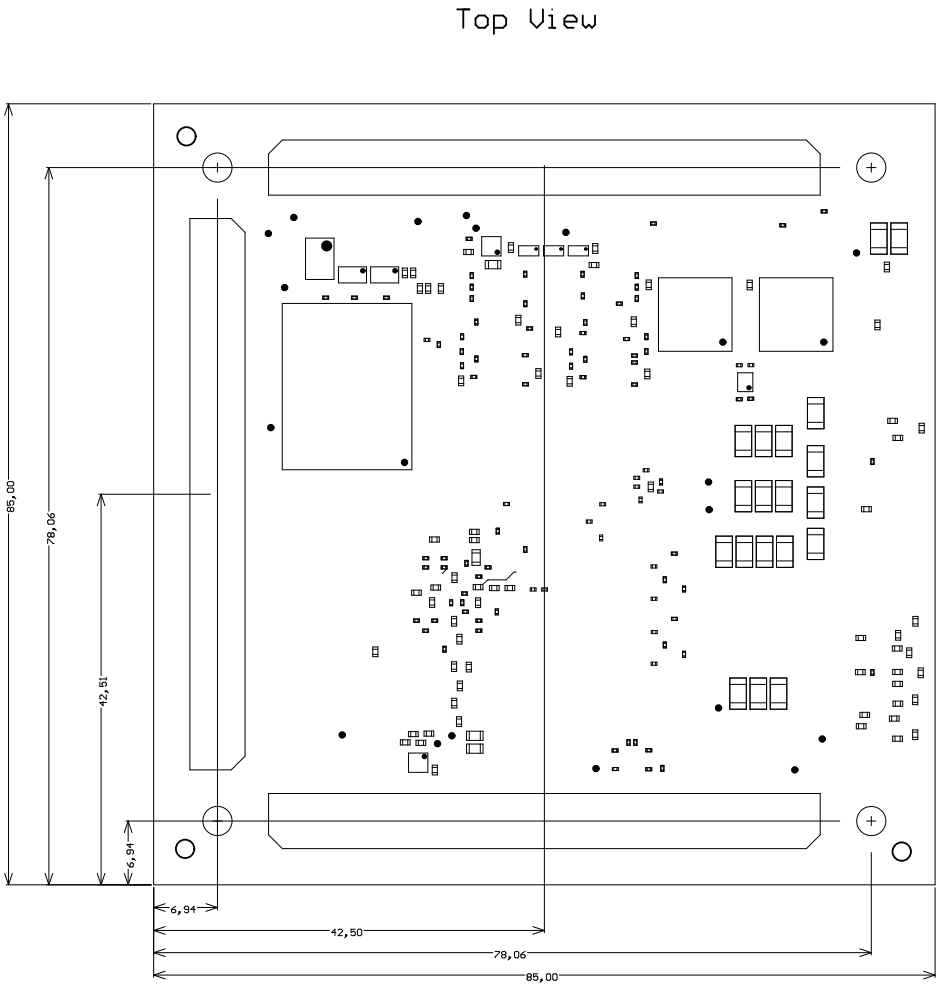
Physical Dimensions
...
Please download the assembly diagram for exact values.
Module size: 85 mm × 85 mm for exact numbers.
Mating height with standard connectors: 8mm5 mm
PCB thickness: 1.6mmHighest part on PCB: approx. 2.5 mm. Please download the step model for exact numbers.,7 mm
All dimensions are shown in mm.
Weigt | Part |
|---|---|
60 g | Plain module |
Temperature Ranges
Commercial grade modules
...
All parts are at least industrial temperature range of -40°C to +85°C. The module operating temperature range depends on customer design and cooling solution. Please contact us for options.
...
Weigt
...
Part
...
g
...
Plain module
...
Document Change History
| date | revision | authors | description |
|---|---|---|---|
| 2016-06-27 | v10 | initial release |
...
Overview
Content Tools