| Scroll Table Layout |
|---|
| orientation | landscape |
|---|
| sortDirection | ASC |
|---|
| repeatTableHeaders | default |
|---|
| sortByColumn | 1 |
|---|
| sortEnabled | false |
|---|
| cellHighlighting | true |
|---|
|
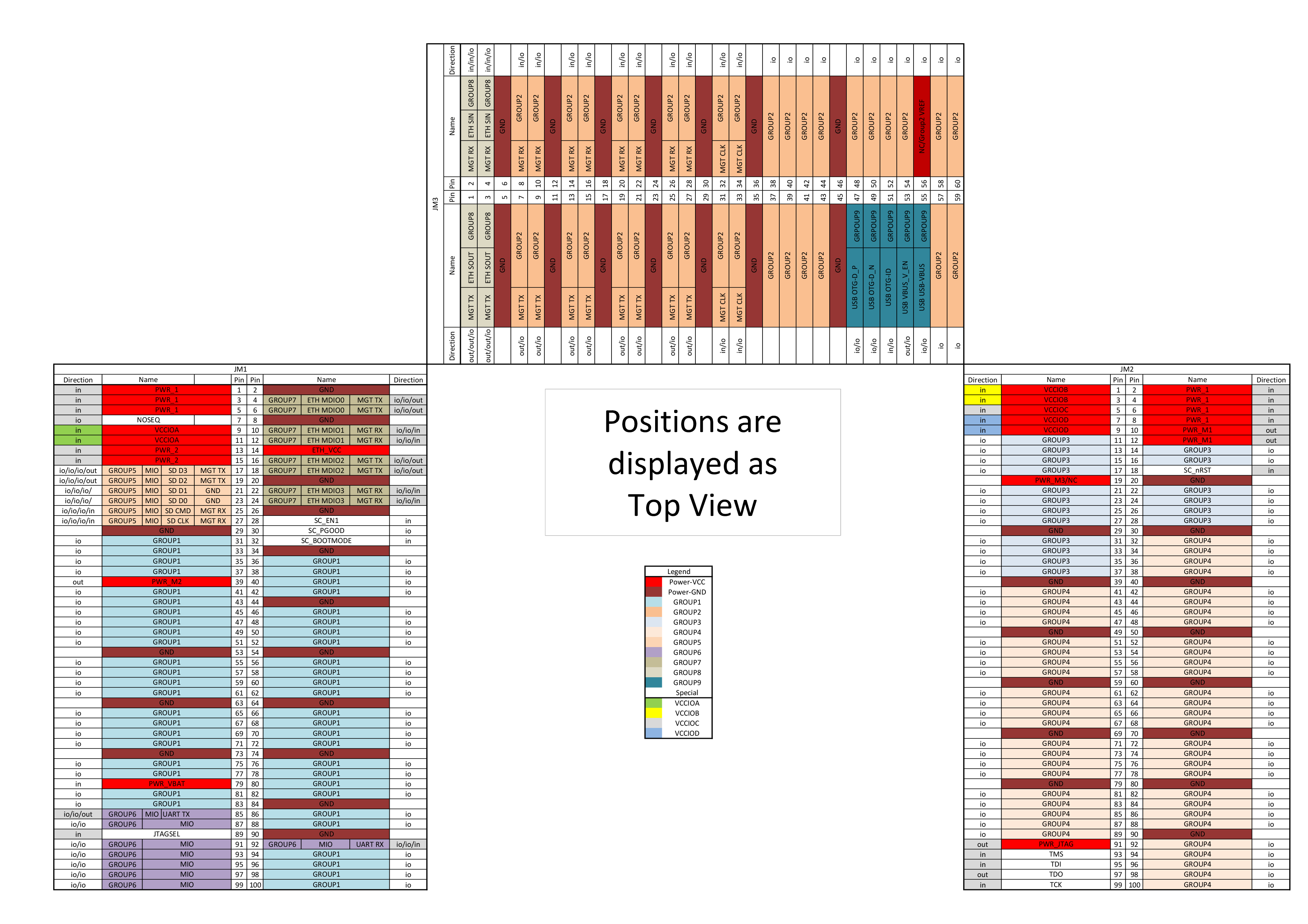
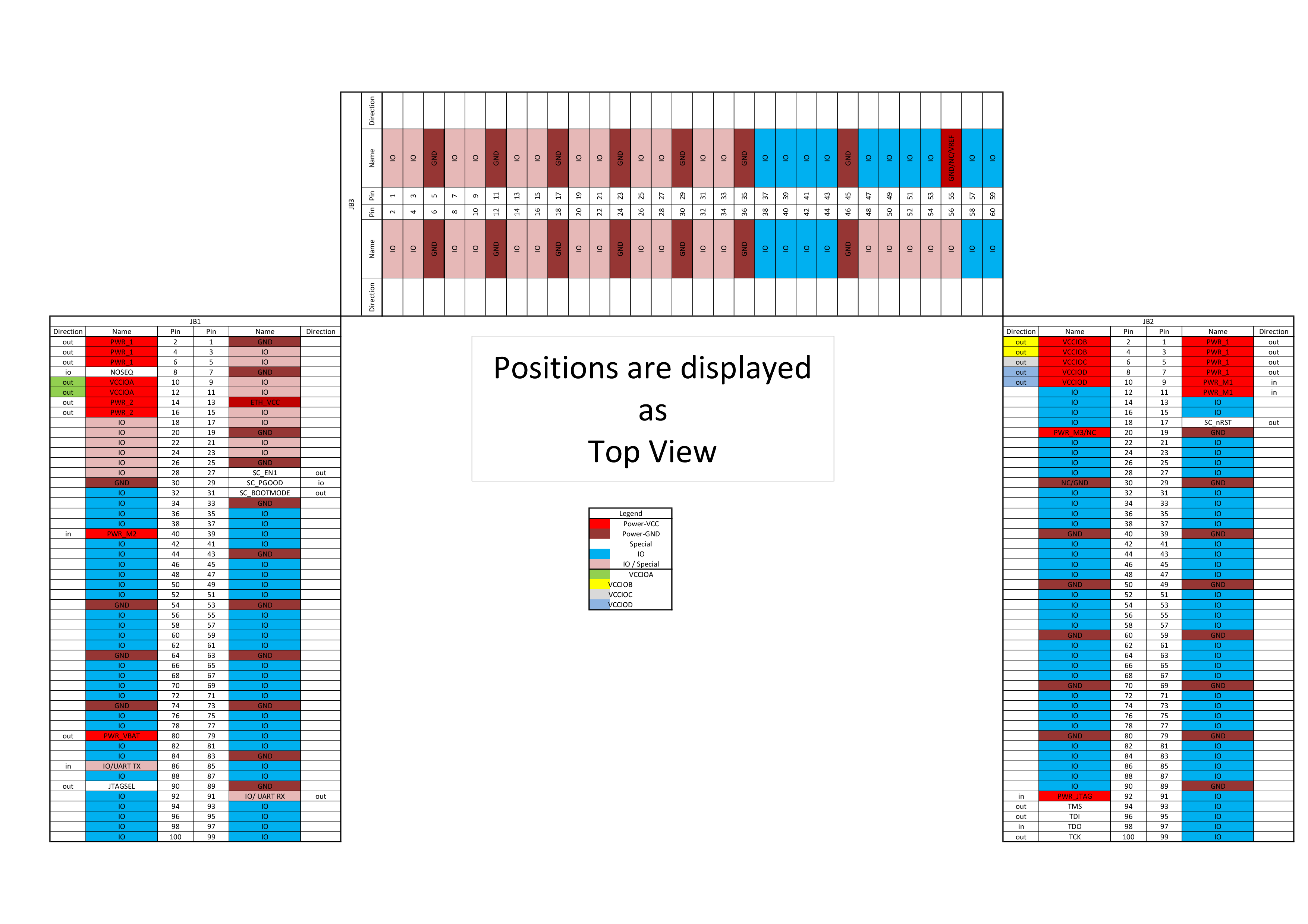
| IO Voltage | B2B Connector | Carrier Boards |
|---|
| Name | Direction* | JB1 | JB2 | TE0701 | TE0703 Rev01 - Rev04 | TE0703 Rev 05 | TE0705 | TE0706 | TEBA0841 | TEBA0841 REV01 | Pin | Pin | Schematic Name | Value,Option,Comp. | Schematic Name | Value,Option,Comp. | Schematic Name | Value,Option,Comp. | Schematic Name | Value,Option,Comp. | Schematic Name | Value,Option,Comp. | Schematic Name | Value,Option,Comp. | Schematic Name | Value,Option,Comp. | | PWR_1 | out | 2,4,6 | 1,3,5,7 | 5V0 | 5V | 3.3V | 3.3V | 3.3V | 3.3V | 5V0 | 5V | 3.3V | 3.3V | 3.3V | use ext. 3.3V power supply | 3.3V | use ext. 3.3V power supply | | VCCIOA | out | 10,12 | VIOTB | FMC_VADJ 2V5 3.3VOUT | VCCIO35 | R23→M3.3VOUT J1B-B1 | VCCIOA | J5→M3.3VOUT, M1.8VOUT R23→M3.3VOUT J1-B1 | VIOTB | FMC_VADJ 2V5 3.3VOUT | VCCIO35 | R20->M3.3VOUT/J6B-B32 | VCCIOA | J26→ M1.8VOUT, 2.5V, 3.3V_OUT J20-6,J20-45 | VCCIOA | J26→ M1.8VOUT, 2.5V, 3.3V_OUT
J20-6,J20-45 | VCCIOD | out | 8,10 | VIOTB | FMC_VADJ 2V5 3.3VOUT | VCCIO13 | R26→M3.3VOUT J2B-B1 | VCCIOD | J10→M3.3VOUT, M1.8VOUT R26→M3.3VOUT J2B-B1 |
| VIOTB | FMC_VADJ 2V5 3.3VOUT | VCCIO13VCCIO35 | R22->M3 R23→M3.3VOUT /J6BJ1B-B1 | VCCIOD | VCCIOA | J5→M3.3VOUT, M1.8VOUT R23→M3.3VOUT J1-B1 | VIOTB | FMC_VADJ 2V5 3.3VOUT | VCCIO35 | R20->M3.3VOUT/J6B-B32 | VCCIOA | J26→ M1.8VOUT, J27→ M1.8VOUT, 2.5V, 3.3V_OUT J17J20-6,J17J20-45 | VCCIODVCCIOA | J27→ J26→ M1.8VOUT, 2.5V, 3.3V_OUT
J17J20-6,J17J20-45PWR_2 | | VCCIOD | out |
| 148,163V3IN10 | VIOTB | FMC_VADJ 2V5 3. 3V3VOUT | VCCIO13 | 3.3V | 3.3V | 3.3V | 3.3V | 3V3IN | 3.3V | 3.3V | 3.3V | 3.3V | use ext. 3.3V power supply | 3.3V | use ext. 3.3V power supply | R26→M3.3VOUT J2B-B1 | VCCIOD | J10→M3.3VOUT, M1.8VOUT R26→M3.3VOUT J2B-B1 | VIOTB | FMC_VADJ 2V5 3.3VOUT | VCCIO13 | R22->M3.3VOUT/J6B-B1 | VCCIOD | J27→ M1.8VOUT, 2.5V, 3.3V_OUT J17-6,J17-45 | VCCIOD | J27→ M1.8VOUT, 2.5V, 3.3V_OUT J17-6,J17-45 | | PWR_2 | out | 14,16 |
| 3V3IN | 3.3V | 3.3V | 3.3V | 3.3V | 3.3V | 3V3IN | 3.3V | 3.3V | 3.3V | 3.3V | use ext. 3.3V power supply | 3.3V | use ext. 3.3V power supply | | VCCIOB | out |
| 2,4 | VCCIOB | out | 2,4 | no name / VIOTA
| FMC_VADJ 2V5 3.3VOUT | VCCIO34 | J5→M3.3VOUT J1B-B32 | VCCIOB | J8→M3.3VOUT,M1.8VOUT J2B-B32 | VIOTB | FMC_VADJ 2V5 3.3VOUT | 1.8V | 1.8V | VCCIOB | J5→ M1.8VOUT, 2.5V, 3.3V_OUT | VCCIOB | NC | VCCIOC | out | 6 | no name / VIOTA
| FMC_VADJ 2V5 3.3VOUT | VCCIO33VCCIO34 | R25→M3J5→M3.3VOUT J2BJ1B-B32 | VCCIOCVCCIOB | J9→M3J8→M3.3VOUT,M1.8VOUT R25→M3.3VOUT J2B-B32 | VIOTB | FMC_VADJ 2V5 3.3VOUT | VCCIO33 | R21->M3.3VOUT | VCCIOC | 1.8V | 1.8V | VCCIOB | J5→ J6→ M1.8VOUT, 2.5V, 3.3V_OUT | VCCIOB | NC | | VCCIOC | NC | PWR_M1 | in | | out |
| 6 | no name / VIOTA
| FMC_VADJ 2V5 9,113.3VOUT 3.3V | VCCIO33 | 3 R25→M3.3VOUT | 3.3V | M3.3VOUT | 3.3V | 3.3VOUT | 3.3V | M3.3VOUT | 3.3V | 3.3V_OUT | 3.3V | J2B-B32 | VCCIOC | J9→M3.3VOUT, M1.8VOUT R25→M3.3VOUT J2B-B32 | VIOTB | FMC_VADJ 2V5 3.3VOUT | VCCIO33 | R21->M3.3VOUT | VCCIOC | J6→ M1.8VOUT, 2.5V, 3.3V_OUT | VCCIOC | 3.3VNC | | PWR_M2M1 | in | 40 | VIOB | 1.8V | M1.8VOUT | 1.8V | M1.8VOUT | 1.8V | VIOB | 1.8V | M1.8VOUT | 1.8V | M1.8VOUT | 1.8V | M1.8VOUT | 1.8V |
| 9,11 | 3.3VOUT | 3.3V | 3.3VOUT | 3.3V | M3.3VOUT | 3.3V | 3.3VOUT | 3.3V | M3.3VOUT | 3.3V | 3.3V_OUT | 3.3V | 3.3V_OUT | 3.3V | | PWR_M2 | in | 40 |
| VIOB | 1.8V | M1.8VOUT | 1.8V | M1.8VOUT | 1.8V | VIOB | 1.8V | M1.8VOUT | 1.8V | M1.8VOUT | 1.8V | M1.8VOUT | 1.8V | | PWR_M3 | in |
| 20 | PWR_M3 | in | 20 | NC | NC |
| NC |
| NC |
| NC |
| NC |
|
| NC |
| NC | | PWR_VBAT | out | 80 |
| VBAT | B1 | VBAT | J7 | VBAT | J7 | NC |
| VBAT | J9 | VBAT | NC | VBAT | NC | | in |
| 92 | VCCJTAG |
| VCCJTAG |
| VCCJTAG |
| VCCJTAG |
| VCCJTAG |
| VCCJTAG |
| VCCJTAG | NC |
Power comparison of all 4x5 carrier boards. *Power direction based on carrier boards view.There are 4 variable user supplied I/O voltages (VCCIOA, VCCIOB, VCCIOC and VCCIOD). PWR_1 and PWR_2 are fixed from carrier boards. PWR_M1 and PWR_M2 normally use default value from module. NC=Not Connected Attention: On some carrier boards the user supplied I/O voltages are connected together (red colored schematic names). |