...
| Scroll Title |
|---|
| title | Module B2B FPGA-Banks and Voltages |
|---|
|
| Scroll Table Layout |
|---|
| orientation | landscape |
|---|
| sortDirection | ASC |
|---|
| repeatTableHeaders | default |
|---|
| sortByColumn | 1 |
|---|
| sortEnabled | false |
|---|
| cellHighlighting | true |
|---|
|
| Group | 1 | 2 | 3 | 4 | 5 | 6 | 7 | 8 | 9 | special |
|---|
| Module Model | Bank | IOs | Type | Voltage | Bank | IOs | Type | Voltage | Bank | IOs | Type | Voltage | Bank | IOs | Type | Voltage | Bank | IOs | Type | Voltage | Bank | IOs | Type | Voltage | Bank | IOs | Type | Voltage |
|
|
| | TE0710 | B15 | 48 | HR | VCCIOA | - | - | - | - | - | - | - | - | B34 | 50 | HR | VCCIOD | B16 | 6 | HR | 3.3V | B14 | 8 | HR | 3.3V | 2x 100Mbit ETH |
|
|
|
|
|
| | TE0711 | B15 | 48 | HR | VCCIOA | B34 | 36 | HR | VCCIOB | B14 | 18 | HR | 3.3V | B35 | 50 | HR | VCCIOD | B16 | 6 | HR | 1.8V | B14 | 8 | HR | 3.3V | B34 | 8 | HR | VCCIOB | B34(4) | USB |
| | TE0712 | B16 | 48 | HR | VCCIOA | B13 | 20 | HR | VCCIOB | B14 | 18 | HR | 3.3V | B15 | 50 | HR | VCCIOD | B13 | 6 | HR | VCCIOB | B14 | 8 | HR | 3.3V | 1x 100Mbit ETH / B13 | 4 | HR | VCCIOB |
| B14 | 4x GTP on G2 | | TE0713 |
|
|
|
|
|
|
|
|
|
|
|
|
|
|
|
|
|
|
|
|
|
|
|
|
|
|
|
|
|
| 4x GTP on G2 | TE0715 -xx-15
with Z-7015
Z-7012S
| B13 | 48 | HR | VCCIOA | B34 | 16 | HR | VCCIOC | B34 | 18 | HR | VCCIOC | B35 | 50 | HR | VCCIOD | B501 | 6 | MIO | 1.8V | B500 | 8 | MIO | 3.3V | 1x Gbit ETH |
|
|
| SGMII | USB | 4x GTP on G2 | TE0715-xx-30
with Z-7030 | B13 | 48 | HR | VCCIOA | B34 | 16 | HP | VCCIOC | B34 | 18 | HP | VCCIOC | B35 | 50 | HP | VCCIOD | B501 | 6 | MIO | 1.8V | B500 | 8 | MIO | 3.3V | 1x Gbit ETH |
|
|
| SGMII | USB | 4x GTP on G2 | | TE0720 | B35 | 48 | HR | VCCIOA | B34 | 36 | HR | VCCIOB | B33 | 18 | HR | VCCIOC | B13 | 50 | HR | VCCIOD | B501 | 6 | MIO | 1.8V | B500 | 8 | MIO | 3.3V | 1x Gbit ETH |
|
|
| SGMII | USB |
| | TE0820* | B66 | 48 | HP | VCCIOA | B65 | 16 | HP | VCCIOC | B65 | 18 | HP | VCCIOC | B64 | 50 | HP | VCCIOD | B501 | 6 | MIO | 3.3V | B501 | 8 | MIO | 3.3V | 1x Gbit ETH |
|
|
| SGMII | USB | 4x GTR on G2 | | TE0821* | B26 | 48 | HD | VCCIOA | B65 | 16 | HP | VCCIOC | B65 | 18 | HP | VCCIOC | B24 | 48 | HD | VCCIOD | B501 | 6 | MIO | 3.3V | B501 | 8 | MIO | 3.3V | 1x Gbit ETH |
|
|
| SGMII | USB | 4x GTR on G2 | | TE0823* | B66 | 48 | HP | VCCIOA | B65 | 16 | HP | VCCIOC | B65 | 18 | HP | VCCIOC | B64 | 50 | HP | VCCIOD | B501 | 6 | MIO | 3.3V | B501 | 8 | MIO | 3.3V | 1x Gbit ETH |
|
|
| SGMII | USB | 4x GTR on G2 | | TE0741 | B13 | 48 | HR | VCCIOA | B16 | 16 | HR | VCCIOB | B15 | 18 | HR | VCCIOC | B12 | 50 | HR | VCCIOD | 1x GTX | 1 Lane |
|
| B14 | 8 | HR | 3.3V | 2x GTX | 2 Lanes |
|
| 1x GTX |
| 4x GTX on G2 | | TE0742* |
|
|
|
|
|
|
|
|
|
|
|
|
|
|
|
|
|
|
|
|
|
|
|
|
|
|
|
|
|
|
| | TE0841 | B64 | 48 | HR | VCCIOA | B66 | 16 | HP | VCCIOB | B68 | 18 | HP | VCCIOC | B67 | 50 | HP | VCCIOD | 1x GTH | 1 Lane |
|
| B65 | 8 | HR | 3.3V | 2x GTH | 2 Lanes |
|
| 1x GTH |
| 4x GTH on G2 | | TE0842* |
|
|
|
|
|
|
|
|
|
|
|
|
|
|
|
|
|
|
|
|
|
|
|
|
|
|
|
|
|
|
|
I/O resource comparison for all 4x5 modules. There are maximum 4 user supplied I/O voltages (VCCIOA, VCCIOB, VCCIOC and VCCIOD). *Attention: Maximum supply voltage for HP banks is 1.8V. |
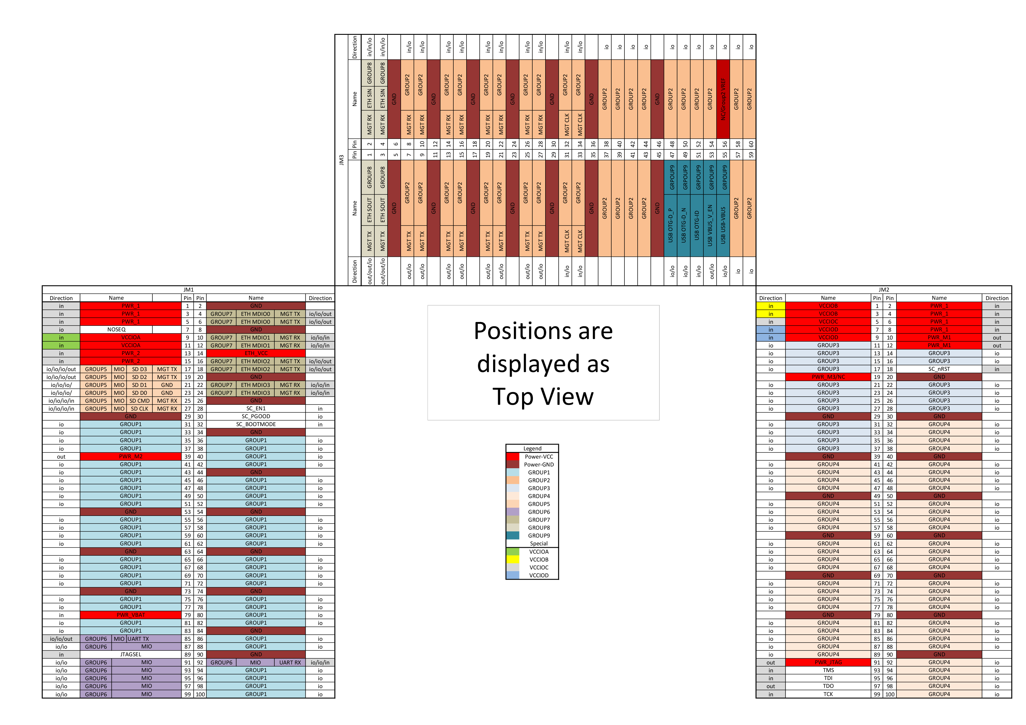
Module Pinout Overview
| Scroll Title |
|---|
| title | Module basic power and group pin assignment, recommended to verify with Schematics |
|---|
|
|
...
| Scroll Title |
|---|
| title | Power Pin Connection on different Carrierboards |
|---|
|
| Scroll Table Layout |
|---|
| orientation | landscape |
|---|
| sortDirection | ASC |
|---|
| repeatTableHeaders | default |
|---|
| sortByColumn | 1 |
|---|
| sortEnabled | false |
|---|
| cellHighlighting | true |
|---|
|
| IO Voltage | B2B Connector | Carrier Boards |
|---|
| Name | Direction* | JB1 | JB2 | TE0701 | TE0703 Rev01 - Rev04 | TE0703 Rev 05 | TE0705 | TE0706 | TEBA0841 | TEBA0841 REV01 |
|
| Pin | Pin | Schematic Name | Value,Option,Comp. | Schematic Name | Value,Option,Comp. | Schematic Name | Value,Option,Comp. | Schematic Name | Value,Option,Comp. | Schematic Name | Value,Option,Comp. | Schematic Name | Value,Option,Comp. | Schematic Name | Value,Option,Comp. | | PWR_1 | out | 2,4,6 | 1,3,5,7 | 5V0 | 5V | 3.3V | 3.3V | 3.3V | 3.3V | 5V0 | 5V | 3.3V | 3.3V | 3.3V | use ext. 3.3V power supply | 3.3V | use ext. 3.3V power supply | | VCCIOA | out | 10,12 |
| VIOTB | FMC_VADJ 2V5 3.3VOUT | VCCIO35 | R23→M3.3VOUT J1B-B1 | VCCIOA | J5→M3.3VOUT, M1.8VOUT R23→M3.3VOUT J1-B1 | VIOTB | FMC_VADJ 2V5 3.3VOUT | VCCIO35 | R20->M3.3VOUT/J6B-B32 | VCCIOA | J26→ M1.8VOUT, 2.5V, 3.3V_OUT J20-6,J20-45 | VCCIOA | J26→ M1.8VOUT, 2.5V, 3.3V_OUT
J20-6,J20-45 | | VCCIOD | out |
| 8,10 | VIOTB | FMC_VADJ 2V5 3.3VOUT | VCCIO13 | R26→M3.3VOUT J2B-B1 | VCCIOD | J10→M3.3VOUT, M1.8VOUT R26→M3.3VOUT J2B-B1 | VIOTB | FMC_VADJ 2V5 3.3VOUT | VCCIO13 | R22->M3.3VOUT/J6B-B1 | VCCIOD | J27→ M1.8VOUT, 2.5V, 3.3V_OUT J17-6,J17-45 | VCCIOD | J27→ M1.8VOUT, 2.5V, 3.3V_OUT J17-6,J17-45 | | PWR_2 | out | 14,16 |
| 3V3IN | 3.3V | 3.3V | 3.3V | 3.3V | 3.3V | 3V3IN | 3.3V | 3.3V | 3.3V | 3.3V | use ext. 3.3V power supply | 3.3V | use ext. 3.3V power supply | | VCCIOB | out |
| 2,4 | no name / VIOTA
| FMC_VADJ 2V5 3.3VOUT | VCCIO34 | J5→M3.3VOUT J1B-B32 | VCCIOB | J8→M3.3VOUT,M1.8VOUT J2B-B32 | VIOTB | FMC_VADJ 2V5 3.3VOUT | 1.8V | 1.8V | VCCIOB | J5→ M1.8VOUT, 2.5V, 3.3V_OUT | VCCIOB | NC | | VCCIOC | out |
| 6 | no name / VIOTA
| FMC_VADJ 2V5 3.3VOUT | VCCIO33 | R25→M3.3VOUT J2B-B32 | VCCIOC | J9→M3.3VOUT, M1.8VOUT R25→M3.3VOUT J2B-B32 | VIOTB | FMC_VADJ 2V5 3.3VOUT | VCCIO33 | R21->M3.3VOUT | VCCIOC | J6→ M1.8VOUT, 2.5V, 3.3V_OUT | VCCIOC | NC | | PWR_M1 | in |
| 9,11 | 3.3VOUT | 3.3V | 3.3VOUT | 3.3V | M3.3VOUT | 3.3V | 3.3VOUT | 3.3V | M3.3VOUT | 3.3V | 3.3V_OUT | 3.3V | 3.3V_OUT | 3.3V | | PWR_M2 | in | 40 |
| VIOB | 1.8V | M1.8VOUT | 1.8V | M1.8VOUT | 1.8V | VIOB | 1.8V | M1.8VOUT | 1.8V | M1.8VOUT | 1.8V | M1.8VOUT | 1.8V | | PWR_M3 | in |
| 20 | NC |
| NC |
| NC |
| NC |
| NC |
|
| NC |
| NC | | PWR_VBAT | out | 80 |
| VBAT | B1 | VBAT | J7 | VBAT | J7 | NC |
| VBAT | J9 | VBAT | NC | VBAT | NC | | in |
| 92 | VCCJTAG |
| VCCJTAG |
| VCCJTAG |
| VCCJTAG |
| VCCJTAG |
| VCCJTAG |
| VCCJTAG | NC |
Power comparison of all 4x5 carrier boards. *Power direction based on carrier boards view.There are 4 variable user supplied I/O voltages (VCCIOA, VCCIOB, VCCIOC and VCCIOD). PWR_1 and PWR_2 are fixed from carrier boards. PWR_M1 and PWR_M2 normally use default value from module. NC=Not Connected Attention: On some carrier boards the user supplied I/O voltages are connected together (red colored schematic names). |
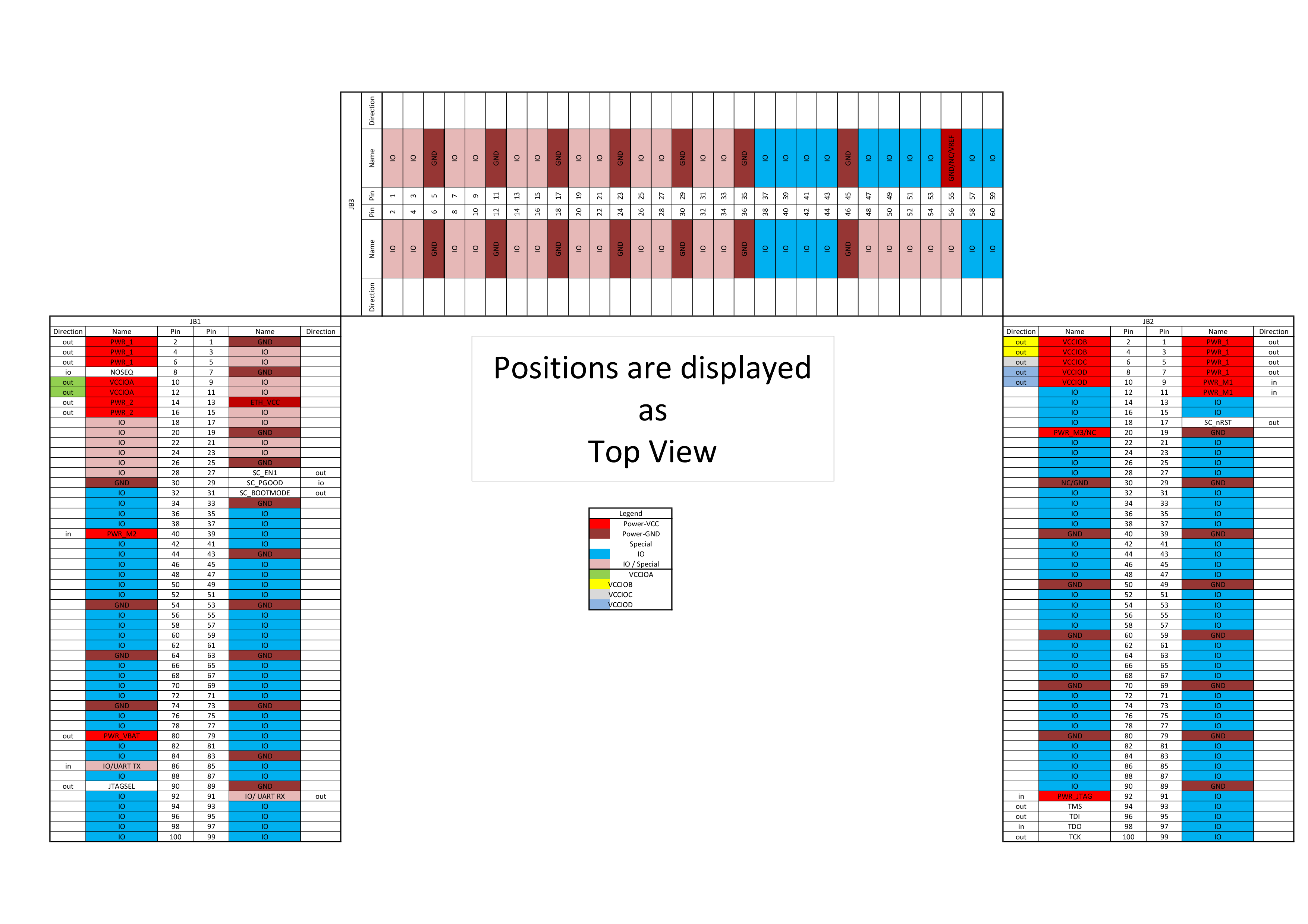
Carrier Pinout Overview
| Scroll Title |
|---|
| title | Carrierboard basic power and group pin assignment (Top View), recommended to verify with Schematics |
|---|
|
|
...
| Scroll Title |
|---|
| title | 4x5 Module Controller IOs |
|---|
|
| Scroll Table Layout |
|---|
| orientation | landscape |
|---|
| sortDirection | ASC |
|---|
| repeatTableHeaders | default |
|---|
| sortByColumn | 1 |
|---|
| sortEnabled | false |
|---|
| cellHighlighting | true |
|---|
|
| Name | Module B2B Pin | Carrier B2B Pin | Direction (Module view) | Description | Recommendation |
|---|
| JTAGSEL | JM1-89 | JB1-90 | in | JTAG Chain multiplexer. Low FPGA, High CPLD. For module with CPLD only. | Connect Pulldown on carrier.
DIP switch possible. | | SC_EN1 | JM1-28 | JB1-27 | in | Module power. Set high to enable module power. Note: Power management depends on module. Sometimes this is a only used as Power ON Reset like SC_nRST | Connect Pullup on carrier.
DIP switch possible | | SC_NOSEQ | JM1-7 | JB1-8 | in / inout | Module Power management. Set high to disable CPLD power management. Note: Power management depends on module and not all modules support extended power management with CPLD. | Connect Pullup or Pulldown force to GND over zero ohm resistor on carrier.
DIP switch possible. | | SC_PGOOD | JM1-30 | JB1-29 | out / inout | Power Good signal. Is Low, if SC_EN1 is set to zero or if power is not ready, otherwise high impedance output. Note: Power management depends on module.
On newer Firmware SC_PGOOD will be used as Additionally Boot Mode Pin. | Connect Pullup on carrier.
Do not use this signal to enable FPGA Bank voltages. It's only for monitoring. To Enable FPGA Banks, use 3.3V(PWR_M1) or 1.8V(PWR_M2) module output. | | SC_BOOTMODE | JM1-32 | JB1-31 | in | Boot Mode selection Pin for Zynq module only. Default low for primary SD boot and high for primary QSPI boot. Note: Depends also on module CPLD firmware | Connect Pullup on carrier.
DIP switch possible. | | SC_nRST | JM2-18 | JB2-17 | in | Low active module reset. Pin force Power one reset on FPGA/SoC. Note: Depending from module CPLD or voltage supervisor is used. | Connect Pullup on carrier.
DIP switch possible. |
|
Remove 4x5 module
| Widget Connector |
|---|
| url | https://www.youtube.com/watch?v=uisv2dWbktc |
|---|
|
...
- Controller IOs are 3.3V IOs
|
Remove 4x5 module
4 x 5 SoMs Handling and Usage Precautions
...
Compatibility Guide
Ethernet LED'S
...
Solution A: connect to 3.3V out from the module, option compatible to all modules except those with HP banks (TE0715-01-30)
Solution B: connect to 1.8V out from the module, option compatible with all modules.
...