Page History
...
See page "4 x 5 cm carriers" to get information about the SoMs supported by the TE0701 Carrier Board.
Main Components
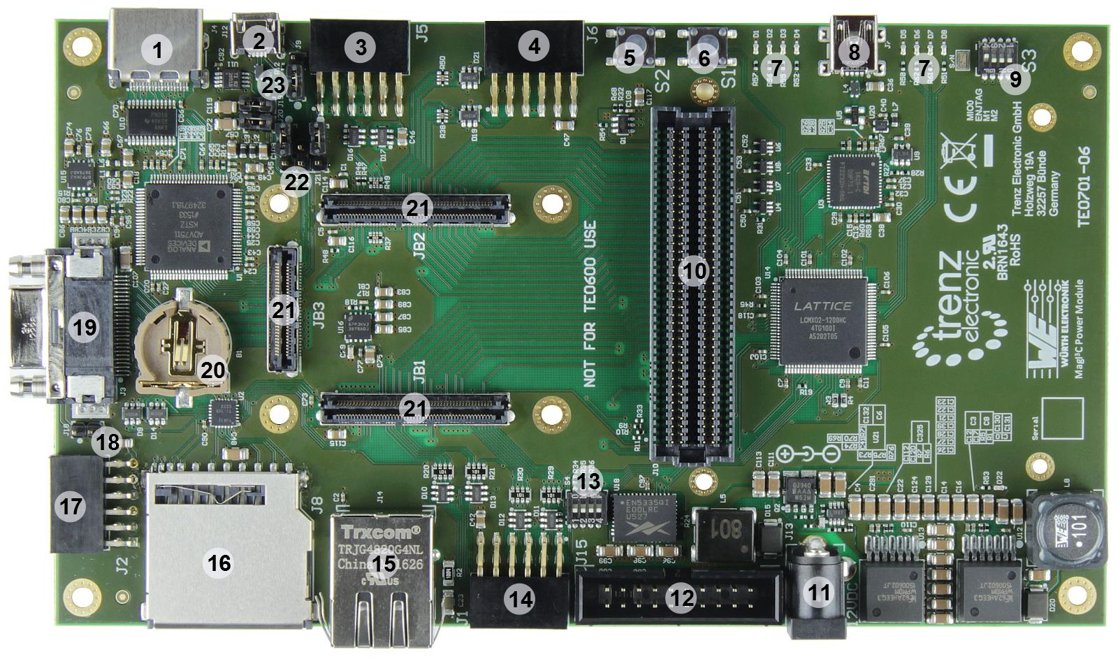
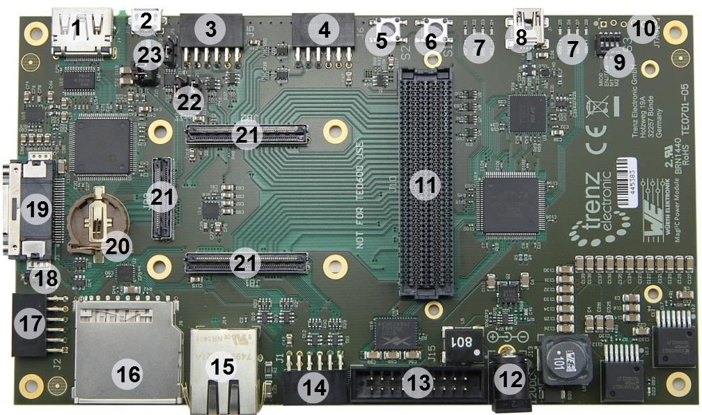
Figure 1: 4x5 SoM carrier board TE0701-0506
TE0701-05 (REV 0506):
- HDMI Connector (1.4 HEAC Support)
- Micro USB Connector (Device, Host or OTG Modes)
Pmod Connector for Zynq-module PL (4 LVDS-pairs, max. VCCIO-Voltage 3,3Vvoltage VIOTA)
- Pmod Connector for Zynq-module PL (4 LVDS-pairs, max. VCCIO-Voltage voltage FMC_VADJ)
- User Push Button S2 ("RESTART" button by default)
- User Push Button S1 ("RESET" button by default)
- User LEDs (function mapping depends on firmware of System-Controller-CPLD)
- Mini USB Connector (USB JTAG and UART Interface)
- User 4-bit DIP Switch
- Direct access to System-Controller-CPLD JTAG-Interface (Solder Pads, pin-strip need to be mounted)
- VITA 57.1 compliant FMC LPC Connector with digitally programmable FMC VADJ Power Supply
- Barrel jack for 12V Power Supply
- ARM JTAG Connector (DS-5 D-Stream) - PJTAG to EMIO multiplexing needed
- User 4-bit DIP Switch (provides the possibility to set voltage FMC_VADJ)
- Pmod Connector (J1, 3.3V): mapped to 8 Zynq PS MIO0-bank-pins (MIO0, MIO9 to MIO15) when using TE0720 (same mapping as on Zedboard), 6 pins (MIO10 to MIO15) are additionally connected to TE0701 System-Controller-CPLD Carrier Controller
- RJ45 GbE Connector
- SD Card Connector - Zynq SDIO0 Bootable SD port
- Pmod Connector (J2, 3.3V): 6 pins (PX0 to PX5) can be multiplexed by Texas Instruments TXS02612RTWR SDIO Port Expander to SD Card pins (MIO1 bank when using TE0720)MIO-pins of Zynq-module, 2 pins are connected to TE0701 System-Controller-CPLD (PX6 and PX7)
- Jumper J18
- Mini CameraLink Connector
- Battery holder for CR1220 (RTC backup voltage)
- Trenz 4x5 module Socket (3x Samtec LSHM Series Connectors)
- Jumper J16, J17, J21
- Jumper J9, J19, J20
...
- Overvoltage-, undervoltage- and reversed- supply-voltage-protection
- Barrel jack for 12V power suppysupply
- Carrier Board System-Controller-CPLD Lattice MachXO2 1200HC, programable by Mini-USB JTAG-Interface J7
- JTAG-Interface of System-Controller-CPLD directly accessible by additional connector J23, pin strip has to be mounted on existing solder pads
- Zynq-module programable by ARM-JTAG-Interface-Connector (J15) or by System-Controller-CPLD via Mini-USB JTAG-Interface J7 or JTAG-Interface on FMC-Connector J10
- Mini CameraLink
- RJ45 Gigabit Ethernet Jack with 2 integrated LEDs.
- FPGA Mezzanine Card (FMC) Connector J10 for acces to Zynq-Module's LVDS-pairs, operable with adjustable IO-voltage FMC_VADJ
- USB JTAG- and UART-Interface (FTDI FT2232HQ) with Mini-USB-Connector J7
- ADV7511 HDMI Transmitter with HDMI-Connector J4
- 8 x user LEDs routed to System-Controller-CPLD, 8 x red
- 2 x user-push button routed to System-Controller-CPLD; by default configured as system "RESET" and "RESTART" button (depends on CPLD-Firmware)
- 2 x 4-bit DIP-Switch for base-board-configuration , (3 switches routed to System-Controller-CPLD, 3 switches to set voltage FMC_VADJ, 1 switch routed to Zynq-module (MIO0), 1 switch enables Mini-USB JTAG-Interface J7
- PMOD-Connectors to access Zynq-Module's LVDS-pairs and MIO-Pins
- Micro SD card socket, can be used to boot system
- Zynq-Module-SDIO-Port also accessible by PMOD-Connector J2 via SDIO Port Expander
- Micro-Micro-USB-Interface (J12) connected to Zynq-module (Device, Host or OTG modes)
- Trenz 4x5 module Socket (3 x Samtec LSHM series connectors)
...
Micro SD Card socket is not directly wired to the B2B connector pins, but through a Texas Instruments TXS02612 SDIO Port Expander, which is needed for voltage translation due to the different voltage levels of the Micro SD Card and MIO-bank 501 of the Xilinx Zynq-module. The Micro SD Card has 3.3V signallingsignal voltage level, but the MIO Bank 501 -bank on the Xilinx Zynq-module chip is set to has VCCIO 1.8V.
The Micro SD Card Socket MIO-bank of the Zynq-module is also accessible by PMOD-Connector J2, which is configurible configurable by the "SEL_SD"-signal of the System-Controller-CPLD. The connector J2 has VCCIO 3.3V.
Dual channel USB to UART/FIFO
...
| Note |
|---|
LED5 (L5) to LED8 (L8) are operating only when the corresponding power supply VIOTB (i.e., bank 1 of the on-board CPLD) is switched on. This can be accomplished on the one hand by connecting the FMC power supply FMC_VADJ to VIOTB (J21: 1,2-3), which is the default option, or on the other hand by connecting either 2.5V (J17: 1,2-3) or 3.3V (J17: 1-2,3) to VIOTB (J21: 1-2,3). Please note that for the first default option, the FMC power supply must be manually switched on set by the , e.g., Zynq FPGA on the TE0720 (user. For detailed information how to set the voltage FMC_VADJ via I2C, please refer to the documentation of the TE0701 Sytem-Controller-CPLD). |
One green LED D22 shows the avaibility availability of the 3.3V supply voltage of the TE0701 Carrier Board.
...
On the TE0701 Carrier Board there are two push buttons (S1 and S2) and are and are routed to the System-Controller-CPLD and available to the user. The default PB mapping of the push buttons is as follows:
| Name | Default Mapping: | ||
|---|---|---|---|
| S1 | If S1 is pushed, the active-low RESet IN (RESIN) signal will be asserted. Note: This reset can also be forced by the FTDI USB-to-JTAG interface. | ||
| S2 | If S2 is pushed, the active-high Power ON (PON) signal (that is internally pulled-up) will be deasserted, which can be considered as a "RESTART" button to switch off (push button) and on (release button) all on-module power supplies (except 3.3VIN). Note: The capability to be enabled the first time will become active shortly after Power on Reset (POR).
|
The functionality of the push buttons depends on the CPLD-firmware. For detailed information of the function of the push buttons, please refer to the documentation of the TE0701 Sytem-Controller-CPLD.
Ethernet
TE0701 has a RJ45 Gigabit Ethernet MAGJACK (J14) with two LED'sLEDs.
On-board Ethernet jack J14 pins are routed to B2B connector JB1. The center tap of the Magnetics is not connected to module's B2B connector.
PHY LED's LEDs are not connected directly to the module's B2B connectors as the 4x5 module have no dedicated PHY LED pins assigned. PHY LED's are connected to the TE0701 System-Controller-CPLD, that can route those LED's to some module's I/O Pins. In that case the module CPLD has to map the PHY LEDs to corresponding pins.With initial Carrier Controller design, one RJ45 LED (the right one) is connected to module NOSEQ pin that functions as PHY LED output on TE0720 with default settings. The other LED is connected to a pin of the I2C-to-GPIO-module and can be controlled by the control register of this module on the Systen-Controller-
CPLD if desiredSee documentation of the TE0701 Sytem-Controller-CPLD to get information of the function of the PYH LEDs.
Pmod Slots
J5 and J6 Pmod signal routing is done as differential pairs for pins 1-2, 3-4, 7-8, 9-10.
Please use Master Pinout Table table as primary reference for the pin mapping information.
...
On the TE0701 carrier boards (TE0701-03 and higher revisions) different hardware/software different VCCIO configurations can be chosen by 6 7 jumpers and one dedicated 4-bit DIP-switch :S4.
The purpose Figure 2 shows the position of the jumpers on the Carrier Board and their default configuration at delivery condition:
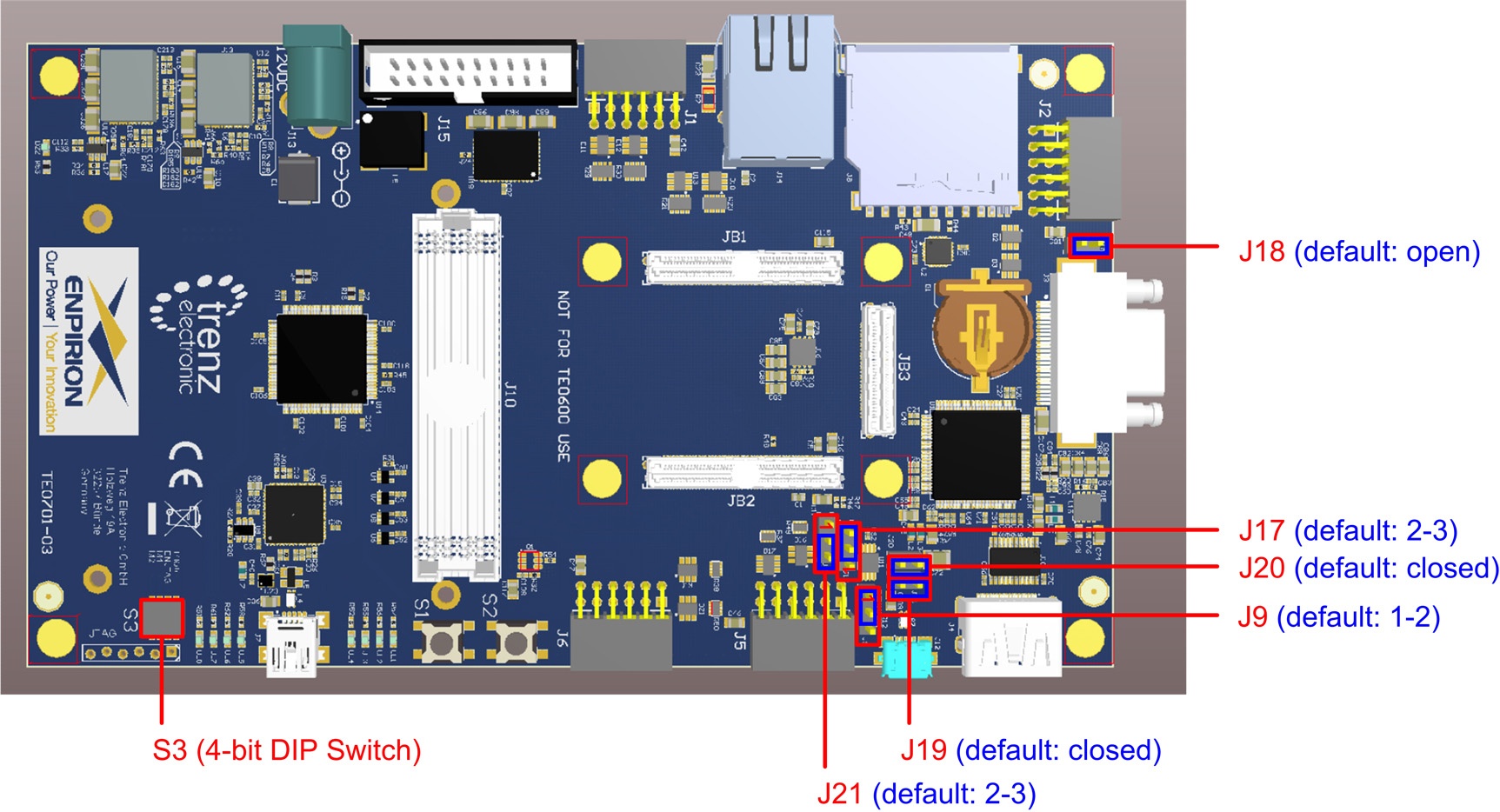
Figure 2: TE0701 Jumper Configurations of TE0701-03 and higher revisions.
The purpose of the jumpers and the DIP switch of the Carrier Board will be explained and the DIP-switch S4 of the Carrier Board will be explained in the following sections.
...
Additionally, the VCCIO33 and VCCIO34 supply voltages of the Zynq FPGA (on bank 33 and bank 34, respectively) can be selected either to be 3.3V (J17:1-2, 3) or 2.5V (J17: 1, 2-3). The latter is the default setting (i.e., VCCIO33=VCCIO34=2.5V). By removing jumper J17 and setting jumper J16 VCCIO33 and VCCIO34 will be set to the adjustable voltage FMC_VADJ.
Furthermore, the VCCIO13 supply voltage (bank 13) can be selected to be either identical to bank 33/34 (J21: 1-2, 3; jumper J16 removed) or to be FMC_VADJ (J21: 1, 2-3). Again, the latter is the default setting (i.e., VCCIO13=FMC_VADJ).
...
| Note |
|---|
There is also the possibility to select fixed FMC_VADJ voltages by the DIP-switch S3S4. Therefore, there is no need to configure any bits on the 8-bit control register of the I2C-to-GPIO-module of the System-Controller-CPLD. Note: Switch S4-4 is routed to the System-Controller-CPLD, the functionality depends on the CPLD-firmware. |
Table 3 shows the switch-configuration of the DIP-switch S3 S4 to set the voltage FMC_VADJ.
Note: The configuration of FMC_VADJ depends on the used firmware of the System-Controller-CPLD. For detailed information, refer to the documentation of the TE0701 Sytem-Controller-CPLD.
S4-1 | S4-2 | S4-3 | M1 | M2 | FMC_VADJ Value |
|---|---|---|---|---|---|
| OFF | OFF | OFF | 13.8V3V | ||
| ON | OFFON | OFF | 2.5V | ||
| OFF | ON | OFF | 31.3V8V | ||
| ON | ON | OFF | 1.5V | ||
| OFF | OFF | ON | I2C Controlled1.25V |
Table 3: Switch S3 S4 positions for fixed values of the FMC_VADJ voltage
Configuring 12V Power Supply Pin on the CameraLink Connector
...
On the TE0701 the 5.0V and 3.3V power supply rails are generated by high performance DC-DC-converters from the external 12V supply. While the 3.3V plane supplies several on-board components (e.g., Lattice CPLD and FTDI Dual USB UART/FIFO IC), the 5V plane is mainly provided for to power supply of the module to be carried (e.g., TE0720 Zynq SoC module). For the latter, however, special considerations must be taken (see TE0720 Power Supply). Therefore, the on-module system controller (SC) must be provided with information about the power-on-reset (POR) process, namely, the following control signals EN1, RESIN, and NOSEQ. And the SC provides, in turn, the status signal PGOOD down to the on-board Sytem-Controller-CPLD.
| Signal | Description | ||
|---|---|---|---|
| EN1 | This CPLD output active-high signal is a “power on (PON)” signal that is usually HIGH (weak pull-up), except, the user push button S2 is pressed, which forces the related signal to be LOW (ground). EN1 enables (EN1=’1’) and disables (EN1=’0’) the power supplies on the carried module, respectively. | ||
| RESIN | This signal is controlled by the user push button S1 on the TE0701 and is forwarded directly to the SC, where it is latched together with the EN1 signal as well as the “all power rails OK” signal (1.0V and 1.8V for core; 1.5V and VTT for RAM, and 3.3V).
When RESIN (alias user push button S1) is not pushed and simultaneously the EN1 signal is asserted (EN='1') and all power rails are ok, the active-high Zynq power-on-reset signal PS_POR_B is asserted. | ||
| NOSEQ | This CPLD signal can be used to enable or disable the power sequencing mode. If the active-high NOSEQ signal is set to HIGH (NOSEQ='1') then the 1.0V and 1.8V power supplies on the carried module will be forced to be enabled. In normal mode (NOSEQ='0') the 3.3V power supply is turned on after the 1.0V and 1.8V supplies have stabilized (see TE0720 Power Supply). The latter is the default mode, i.e., for the NOSEQ pin of the SC the internal pull-down is activated. After booting, the NOSEQ pin can be used as general-purpose I/O pin. For example, the SC (REV 0.02) maps the Ethernet PHY LED0 to NOSEQ by default. However, this mapping can be changed by software after boot. | ||
| PGOOD | This active-high signal (with internal pull-up) is a status input to the CPLD about the current status of the power supply rails on the carried module (e.g., TE0720). It is routed to user LED3, which is switched on when the on-module power supply rails are not ok. |
...
All dimensions are given in mm.
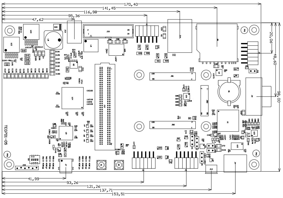
Figure 3: Physical Dimensions of the TE0701-05 carrier board
Operating Temperature Ranges
...
| date | revision | authors | description |
|---|---|---|---|
| 2016-11-29 | Ali Naseri | TRM update due to new revision 06 of the carrier board. | |
| 2016-11-28 | 1.0 | Ali Naseri | TRM adjustment to the newest revision (05) of TE0701 Carrier Board. |
| 2014-02-18 | 0.2
| Sven-Ole Voigt | TE0701-03 (REV3) updated |
| 2014-01-05 | 0.1 | Sven-Ole Voigt | Initial release |
All |
...
| Date | Revision | Notes | PCN | Documentation link |
|---|---|---|---|---|
| - | 01 | Prototype | ||
| - | 02 | Prototype | ||
| - | 03 | changed DC/DC converters | ||
| - | 04 | |||
| - | 05 | improved manufacturing | TRM-TE0701-05 | |
| - | 06 | additional Jumper J16 and switch S4 for setting VCCIO FMC_VADJ. |
Figure 4: Hardware revisionn revision Number
Hardware revision number is printed on the PCB board next to the module model number separated by the dash.
...
Overview
Content Tools