Page History
| Scroll Ignore |
|---|
Download PDF version of this document.
|
| Scroll pdf ignore | |
|---|---|
Table of Contents
|
...
Programmable unit | Content | Notes |
|---|---|---|
| Xilinx Artix-7 FPGA | Not programmed | U1 |
| System Controller CPLD | Programmed | U3 |
| SPI Flash OTP area | Empty | U4 |
SPI Flash main array | Empty | U4 |
| SPI Flash Quad Enable bit | Set | U4 |
Microchip 11AA02E48 | Globally unique EUI-48 (Ethernet MAC address) | U7 |
| Programmable quad clock generator, Silicon Labs Si5338 | Programmed, CLK1A - 50M, CLK2 - 125M, CLK3 - 50M | U2 |
Signals, Interfaces and Pins
...
The Si5338 can be programmed to change the output frequency of the FPGA clocks (the Ethernet clock must remain at 50 MHz). An I2C bus is connected between the FPGA (master) and clock generator (slave). Proper logic needs to be created in the FPGA to exercise the I2C bus with the correct data. See the reference design section for more information.
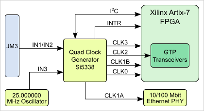
| CLK Output | FPGA Bank | FPGA Pin | IO Standard | Net Name | Default Frequency REV 01, REV 02 | Default Frequency REV 03 and higher | Notes |
|---|---|---|---|---|---|---|---|
| CLK0 | 35 | K4/J4 | DIFF_SSTL15 | CLK0_P/N |
| Off | 100MHz LVDS18 | NB! Since PCB REV02. | |||||
| CLK1A | - | - | CLK50M | 50 MHz | 50MHz CMOS33 | PHY chip RMII reference clock. | |
| CLK1B | 34 | R4 | CLK50M2 | Off |
50MHz CMOS33 | NB! Since PCB REV02. | ||||||
| CLK2 | 216 | F6/E6 | Auto | MGT_CLK0_P/N | 125 MHz | 125MHz LVDS18 | GTP transceiver clock. |
| CLK3 | 35 | H4/G4 | DIFF_SSTL15 | PLL_CLK_P/N | 50 MHz | 50MHz LVDS18 |
Certain B2B connector pins are connected to the FPGA pins which are capable of handling clocking signals from the user’s PCB (baseboard). See schematics B2B page for additional information.
...
| Parameter | Min | Max | Units | Reference Document |
|---|---|---|---|---|
| VIN supply voltage | 2.4 | 5.5 | V | EP53F8QI datasheet. |
| 3.3VIN supply voltage | 2.9 | 5.5 | V | TPS748 datasheet. |
| HR I/O banks supply voltage (VCCO) | 1.14 | 3.465 | V | Xilinx datasheet DS181 |
| HR I/O banks input voltage | -0.20 | VCCO + 0.2 | V | Xilinx datasheet DS181 |
Operating Temperature Ranges
Commercial grade: 0°C to +70°C.
Industrial grade: -40°C to +85°C.
Operating temperature range depends also on customer design and cooling solution. Please contact us for options.
| Note |
|---|
| Assembly variants for higher storage temperature range are available on request. |
| Page break |
|---|
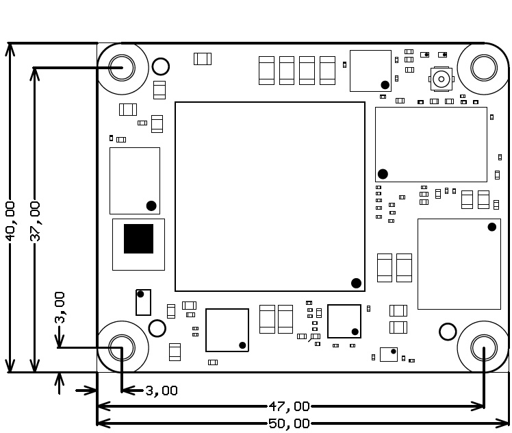
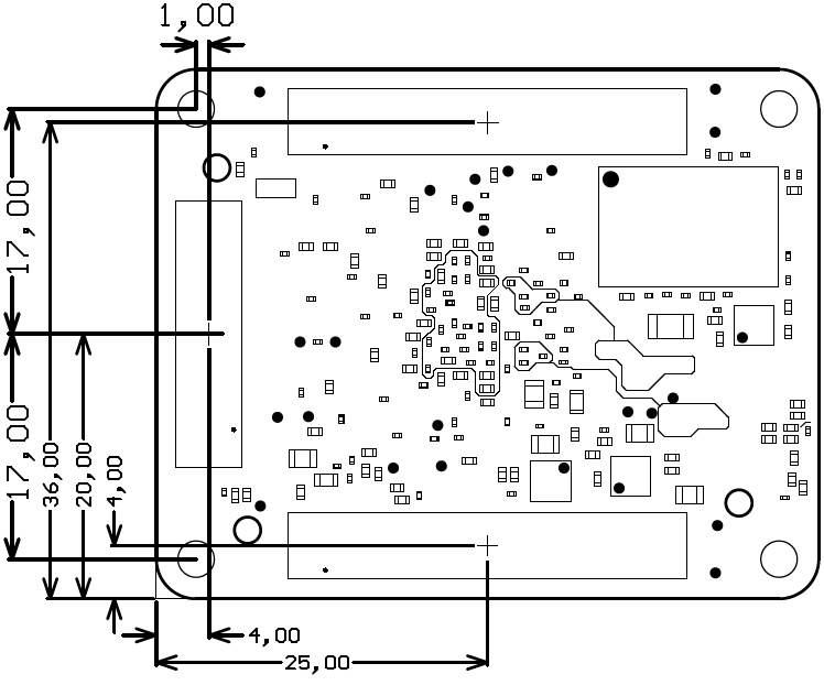
Physical Dimensions
- Module size: 50 mm × 40 mm. Please download the assembly diagram for exact numbers.
- Mating height with standard connectors: 8mm
- PCB thickness: 1.6mm
- Highest part on PCB: approx. 2.5mm. Please download the step model for exact numbers.
All dimensions are shown in millimeters.
Weight
16 - 27 g, Plain module (depends on variant).8.8 g, Set of nuts and bolts.variant).
8.8 g, Set of nuts and bolts.
Currently Offered Variants
| Page properties | ||||
|---|---|---|---|---|
| ||||
Set correct link to the shop page overview table of the product on English and German. Example for TE0706: ENG Page: https://shop.trenz-electronic.de/en/search?sSearch=TE0706 DEU Page: https://shop.trenz-electronic.de/de/search?sSearch=TE0706 |
| Scroll Title | ||||||||||||||||||||||
|---|---|---|---|---|---|---|---|---|---|---|---|---|---|---|---|---|---|---|---|---|---|---|
| ||||||||||||||||||||||
| ||||||||||||||||||||||
Revision History
Hardware Revision History
...
Date | Revision | Contributors | Description | ||||||||||||||||||||||||||
|---|---|---|---|---|---|---|---|---|---|---|---|---|---|---|---|---|---|---|---|---|---|---|---|---|---|---|---|---|---|
|
|
| Updated Download link for this document | ||||||||||||||||||||||||||
2022-12-22 | v.31 |
| |||||||||||||||||||||||||||
| 2020-07-03 | v.23 | John Hartfiel |
| ||||||||||||||||||||||||||
| 2019-01-10 | v.22 | John Hartfiel |
| ||||||||||||||||||||||||||
| 2017-12-15 | v.18 | John Hartfiel |
| ||||||||||||||||||||||||||
| 2017-12-12 | v.15 | John Hartfiel |
| ||||||||||||||||||||||||||
| 2017-05-29 | v.13 | Jan Kumann |
| ||||||||||||||||||||||||||
| 2017-03-01 | v.7 | John Hartfiel |
| ||||||||||||||||||||||||||
| 2017-01-26 | v.3 | Jan Kumann |
| ||||||||||||||||||||||||||
| 2017-01-20 | v.2 | Jan Kumann |
| ||||||||||||||||||||||||||
| 2013-12-02 | v.1 | Antti Lukats |
| ||||||||||||||||||||||||||
| -- | all |
|
|
Disclaimer
| Include Page | ||||
|---|---|---|---|---|
|
Overview
Content Tools