Table of Contents
Overview
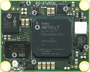
Trenz Electronic TE0712 is an industrial-grade FPGA module integrating a Xilinx Artix-7 FPGA, a 10/100 Mbit Ethernet transceiver, 1 GByte of DDR3 SDRAM, 32 MByte Flash memory for configuration and operation, and powerful switching-mode power supplies for all on-board voltages. Numerous configurable I/Os are provided via rugged high-speed strips. All this on a tiny footprint, smaller than a credit card size at very competitive price. All Trenz Electronic SoMs in 4 x 5 cm form factor are mechanically compatible.
Key Features
- Xilinx Artix-7 FPGA (15T to 200T) supported by the free Xilinx Vivado WebPACK software
- Both industrial and commercial temperature ranges available
- Rugged for high shock resistance and high vibration
- 1 GByte DDR3 32-bit SDRAM
- 10/100 Mbit Ethernet PHY
- MAC address EEPROM
- 32 MByte QSPI Flash memory (with XiP support)
- Programmable clock generator
- Transceiver clock (default 125 MHz)
- Fabric clock (default 200 MHz)
- Transceiver clock (default 125 MHz)
- Plug-on module with 2 × 100-pin and 1 × 60-pin high-speed hermaphroditic strips
- 158 FPGA I/Os (78 differential pairs) available via board-to-board connectors (quantity depends on assembly variant)
- 4 GTP (high-performance transceiver) lanes
- GTP (high-performance transceiver) clock input
- On-board high-efficiency DC-DC converters
- 12A x 1.0V power rail
- 1.5A x 1.8V power rail
- 1.5A x 1.5V power rail
- System management and power sequencing
- eFUSE bit-stream encryption
- AES bit-stream encryption
- User configurable LEDs
- Evenly-spread supply pins for good signal integrity
Additional assembly options are available for cost or performance optimization upon request.
Block Diagram
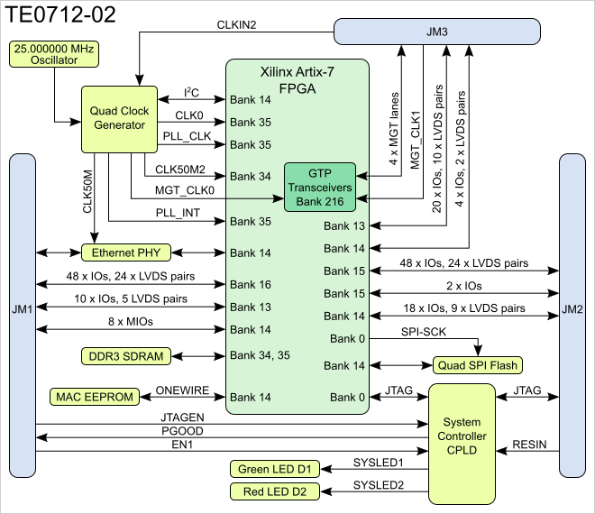
Main Components
Programmable oscillator @25 MHz, SiTime SiT8008, U9
Programmable quad clock generator, Silicon Labs Si5338, U2
10/100 Mbps Ethernet PHY transceiver, Texas Instruments TLK106, U5
Xilinx Artix-7 FPGA XC7A series, U1
32 MByte QSPI Flash memory, Cypress S25FL256S, U4
4 Gbit DDR3 SDRAM, Intelligent Memory IM4G16D3EABG, U15
System Controller CPLD, Lattice Semiconductor MachXO2-256HC, U3
4 Gbit DDR3 SDRAM, Intelligent Memory IM4G16D3EABG, U19
Serial EEPROM, Microchip 11AA02E48, U7
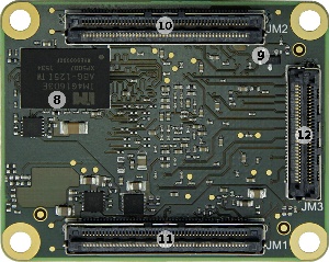
- Samtec Razor Beam™ LSHM-150 B2B connector, JM2
- Samtec Razor Beam™ LSHM-150 B2B connector, JM1
- Samtec Razor Beam™ LSHM-150 B2B connector, JM3
- 12A Enpirion EN63A0QI PowerSoC DC-DC converter, U14
- Green LED (SYSLED1), D1
- Red LED (SYSLED2), D2
Initial Delivery State
Programmable unit | Content | Notes |
|---|---|---|
| Xilinx Artix-7 FPGA | Not programmed | U1 |
| System Controller CPLD | Programmed | U3 |
| SPI Flash OTP area | Empty | U4 |
SPI Flash main array | Empty | U4 |
| SPI Flash Quad Enable bit | Set | U4 |
Microchip 11AA02E48 | Globally unique EUI-48 (Ethernet MAC address) | U7 |
| Programmable quad clock generator, Silicon Labs Si5338 | Programmed, CLK1A - 50M, CLK2 - 125M, CLK3 - 50M | U2 |
Signals, Interfaces and Pins
Board to Board (B2B) I/Os
FPGA bank number and number of I/O signals connected to the B2B connector:
| FPGA Bank | B2B Connector | I/O Signal Count | Voltage Level | Notes |
|---|---|---|---|---|
| 13 | JM1 | 10 | VCCIO13 | Supplied by the baseboard. Not available on XC7A35T assembly variant. |
| 13 | JM3 | 20 | VCCIO13 | Supplied by the baseboard. Not available on XC7A35T assembly variant. |
| 14 | JM1 | 8 | 3.3V | |
| 14 | JM2 | 18 | 3.3V | |
| 14 | JM3 | 4 | 3.3V | |
| 15 | JM2 | 48 | VCCIO15 | Supplied by the baseboard. |
| 15 | JM2 | 2 | VCCIO15 | Supplied by the baseboard. |
| 16 | JM1 | 48 | VCCIO16 | Supplied by the baseboard. |
Please refer to the Pin-out tables page for additional information.
JTAG Interface
JTAG access to the Xilinx Artix-7 FPGA and System Controller CPLD devices is provided through B2B connector JM2.
JTAG Signal | B2B Pin |
|---|---|
| TMS | JM2-93 |
| TDI | JM2-95 |
| TDO | JM2-97 |
| TCK | JM2-99 |
JTAGEN pin in B2B connector JM1 is used to select JTAG access for FPGA or SC CPLD:
| JTAGEN | JTAG Access To |
|---|---|
| Low | Artix-7 FPGA |
| High | System Controller CPLD |
System Controller I/O Pins
Special purpose pins are connected to System Controller CPLD and have following default configuration:
| Pin Name | Mode | Function | Default Configuration |
|---|---|---|---|
| PGOOD | INOUT | Power good | Active low when EN1 is low or module power is invalid otherwhise high impedance |
| JTAGEN | Input | JTAG select | Low for normal operation, high for System Controller CPLD access. |
| EN1 | Input | Power Enable | When forced low, pulls POR_B low to emulate power on reset. |
| NOSEQ | - | No function | Not used. |
| MODE | - | No function | Not used. |
Purpose of this IOs depends in the CPLD Firmware, please check also CPLD Firmware description, see: TE0712 CPLD
On-board LEDs
The TE0712 module has 2 LEDs which are connected to the System Controller CPLD. Once FPGA configuration has completed these can be used by the user's design.
| LED | Color | SC Signal | SC Pin | Notes |
|---|---|---|---|---|
| D1 | Green | SYSLED1 | 9 | Exact function depends on System Controller CPLD firmware. |
| D2 | Red | SYSLED2 | 8 | Exact function depends on System Controller CPLD firmware. |
Clocking
Si5338 programmable clock generator is used to generate different clocks with 25 MHz oscillator connected to pin IN3. The Si5338 can alternatively be clocked using pins IN1 and IN2 which are connected to B2B connector JM3 (CLKIN2).
The Si5338 can be programmed to change the output frequency of the FPGA clocks (the Ethernet clock must remain at 50 MHz). An I2C bus is connected between the FPGA (master) and clock generator (slave). Proper logic needs to be created in the FPGA to exercise the I2C bus with the correct data. See the reference design section for more information.
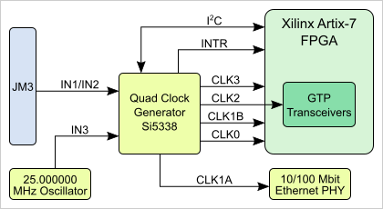
| CLK Output | FPGA Bank | FPGA Pin | IO Standard | Net Name | Default Frequency REV 01, REV 02 | Default Frequency REV 03 and higher | Notes |
|---|---|---|---|---|---|---|---|
| CLK0 | 35 | K4/J4 | DIFF_SSTL15 | CLK0_P/N | Off | 100MHz LVDS18 | NB! Since PCB REV02. |
| CLK1A | - | - | CLK50M | 50 MHz | 50MHz CMOS33 | PHY chip RMII reference clock. | |
| CLK1B | 34 | R4 | CLK50M2 | Off | 50MHz CMOS33 | NB! Since PCB REV02. | |
| CLK2 | 216 | F6/E6 | Auto | MGT_CLK0_P/N | 125 MHz | 125MHz LVDS18 | GTP transceiver clock. |
| CLK3 | 35 | H4/G4 | DIFF_SSTL15 | PLL_CLK_P/N | 50 MHz | 50MHz LVDS18 |
Certain B2B connector pins are connected to the FPGA pins which are capable of handling clocking signals from the user’s PCB (baseboard). See schematics B2B page for additional information.
On-board Peripherals
32 MByte Quad SPI Flash Memory
On-board QSPI flash memory S25FL256S (U14) is used to store initial FPGA configuration. Besides FPGA configuration, remaining free flash memory can be used for user application and data storage. All four SPI data lines are connected to the FPGA allowing x1, x2 or x4 data bus widths. Maximum data rate depends on the selected bus width and clock frequency used.
SPI Flash QE (Quad Enable) bit must be set to high or FPGA is unable to load its configuration from flash during power-on. By default this bit is set to high at the manufacturing plant.
System Controller CPLD
System Controller CPLD (Lattice MachXO2-256HC, U3) is used to control FPGA configuration process. The FPGA is held in reset (by driving the PROG_B signal low) until all power supplies have stabilized.
By driving signal RESIN to low you can reset the FPGA. This signal can be driven from the user’s baseboard PCB via the B2B connector JM2 pin 18.
Input EN1 is also gated to FPGA reset, should be open or pulled up for normal operation. By driving EN1 low, on-board DC-DC converters will be not turned off.
User can create their own System Controller design using Lattice Diamond software. Once created it can be programmed into CPLD via JTAG interface.
DDR3 SDRAM
The TE0712-02 SoM has two 4 Gbit volatile DDR3 SDRAM ICs (U15 and U19) for storing user application code and data.
- Part number: IM4G16D3FABG-125I
- Supply voltage: 1.5V
- Organization: 32M words x 16 bits x 8 banks
- Memory speed: limited by Xilinx Artix-7 speed grade and MIG
Configuration of the DDR3 memory controller in the FPGA should be done using the MIG tool in the Xilinx Vivado Design Suite IP catalog.
Ethernet PHY
The 10/100 Mbps Ethernet PHY TLK106 (U5) by Texas Instruments is connected to the FPGA bank 14 using Reduced Media Independent Interface standard (RMII). The RMII standard has reduced set of data lines (two rather than four) and a higher clock frequency (50 MHz rather than 25 MHz) compared to the Media Independent Interface standard (MII). A management interface is also available allowing access to registers in the PHY chip. Transmit and receive signals are connected to the B2B connector JM1. The magnetics and RJ-45 jack must be placed on the user's PCB (baseboard).
FPGA Ethernet Signals
| FPGA Pin | Signal Name | Signal Description |
|---|---|---|
| N17 | ETH-RST | Ethernet reset, active-low. |
| N15 | LINK_LED | Ethernet LED pin indication mode: in mode 1 - LINK, in mode 2 - ACT. |
| R16 | MDC | Ethernet management clock. |
| P17 | MDIO | Ethernet management data. |
| P14 | ETH_TX_D0 | Ethernet transmit data 0. Output to Ethernet PHY. |
| P15 | ETH_TX_D1 | Ethernet transmit data 1. Output to Ethernet PHY. |
| R14 | ETH_TX_EN | Ethernet transmit enable. |
| N13 | ETH_RX_D0 | Ethernet receive data 0. Input from Ethernet PHY. |
| N14 | ETH_RX_D1 | Ethernet receive data 0. Input from Ethernet PHY. |
| P20 | ETH_RX_DV | Ethernet receive data valid. |
All signals are connected to the FPGA bank 14 and correspond to LVCMOS33 standard.
MAC Address EEPROM
TE0712-02 module has a 2 Kbit Serial Electrically Erasable PROM (EEPROM, U7). It provides pre-programmed 48-bit Extended Unique Identifier (EUI-48™) to identify network hardware MAC address which is write-protected to ensure tamper-proof designs. This SEEPROM can be accessed by UNI/O® serial interface bus using Manchester encoding techniques. The clock and data are combined into a single, serial bit stream (SCIO), where the clock signal is extracted by the receiver to correctly decode the timing and value of each bit. The bus is controlled by a master device (Xilinx Artix-7) which determines the clock period, controls the bus access and initiates all operations, while the SEEPROM works as a slave. Refer to Microchip's 11AA02E48 datasheet for more information.
Power and Power-On Sequence
Power Supply
Single 3.3V power supply (for both VIN and 3.3VIN power rails) with minimum current capability of 3A for system startup is recommended.
Power Consumption
Typical module power consumption is between 2-3W. Exact power consumption is to be determined.
TE0712-02 module can also be powered by split 5V/3.3V power sources if preferred. In such case apply 5V to B2B connectors VIN pins and 3.3V to 3.3VIN pins, although lowest power consumption is achieved when powering the module from single 3.3V supply. When using split 5V/3.3V supplies the power consumption (and heat dissipation) will rise due to the DC-DC converter efficiency (it decreases when VIN/VOUT ratio rises).
Power-On Sequence
For the highest efficiency of the on-board DC-DC regulators, it is recommended to use same 3.3V power source for both VIN and 3.3VIN power rails. Although VIN and 3.3VIN can be powered up in any order, it is recommended to power them up simultaneously.
It is important that all baseboard I/Os are 3-stated at power-on until 3.3V is present on B2B connector JM2 pins 10 and 12, meaning that all on-module voltages have become stable and module is properly powered up.
See Xilinx datasheet DS181 - "Artix-7 FPGAs Data Sheet: DC and AC Switching Characteristics" for additional information. User should also check related baseboard documentation when choosing baseboard design for TE0712 module.
3.3Vout or 1.8Vout from the module can be used to enable power supply for variable bank power and periphery, see also
4 x 5 SoM Integration Guide#4x5SoMIntegrationGuide-4x5ModuleControllerIOs
Power Rails
Power Rail Name | B2B Connector JM1 Pin | B2B Connector JM2 Pin | Direction | Notes |
|---|---|---|---|---|
VIN | 1, 3, 5 | 2, 4, 6, 8 | Input | SoM supply voltage (from the baseboard). |
| 3.3VIN | 13, 15 | - | Input | SoM supply voltage (from the baseboard). |
| 1.5V | - | 19 | Output | Module internal 1.5V level. |
1.8V | 39 | - | Output | Module internal 1.8V level. Maximum 300mA available. |
| 3.3V | - | 10, 12 | Output | Module internal 3.3V level. |
| 3.3V | 14 | Output | Module internal 3.3V level. Not on all 4x5 modules | |
| VCCIO13 | - | 1, 3 | Input | High-Range bank supply voltage (from the baseboard). |
| VCCIO15 | - | 7, 9 | Input | High-Range bank supply voltage (from the baseboard). |
| VCCIO16 | 9, 11 | - | Input | High-Range bank supply voltage (from the baseboard). |
| VREF_JTAG | - | 91 | Output | JTAG reference voltage (3.3V). |
Board to Board Connectors
These connectors are hermaphroditic. Odd pin numbers on the module are connected to even pin numbers on the baseboard and vice versa.
4 x 5 modules use two or three Samtec Razor Beam LSHM connectors on the bottom side.
- 2 x REF-189016-02 (compatible to LSHM-150-04.0-L-DV-A-S-K-TR), (100 pins, "50" per row)
- 1 x REF-189017-02 (compatible to LSHM-130-04.0-L-DV-A-S-K-TR), (60 pins, "30" per row) (depending on module)
Connector Mating height
When using the same type on baseboard, the mating height is 8mm. Other mating heights are possible by using connectors with a different height
| Order number | Connector on baseboard | compatible to | Mating height |
|---|---|---|---|
| 23836 | REF-189016-01 | LSHM-150-02.5-L-DV-A-S-K-TR | 6.5 mm |
| LSHM-150-03.0-L-DV-A-S-K-TR | LSHM-150-03.0-L-DV-A-S-K-TR | 7.0 mm | |
| 23838 | REF-189016-02 | LSHM-150-04.0-L-DV-A-S-K-TR | 8.0 mm |
| LSHM-150-06.0-L-DV-A-S-K-TR | LSHM-150-06.0-L-DV-A-S-K-TR | 10.0mm | |
| 26125 | REF-189017-01 | LSHM-130-02.5-L-DV-A-S-K-TR | 6.5 mm |
| LSHM-130-03.0-L-DV-A-S-K-TR | LSHM-130-03.0-L-DV-A-S-K-TR | 7.0 mm | |
| 24903 | REF-189017-02 | LSHM-130-04.0-L-DV-A-S-K-TR | 8.0 mm |
| LSHM-130-06.0-L-DV-A-S-K-TR | LSHM-130-06.0-L-DV-A-S-K-TR | 10.0mm |
Connectors.
The module can be manufactured using other connectors upon request.
Connector Speed Ratings
The LSHM connector speed rating depends on the stacking height; please see the following table:
| Stacking height | Speed rating |
|---|---|
| 12 mm, Single-Ended | 7.5 GHz / 15 Gbps |
| 12 mm, Differential | 6.5 GHz / 13 Gbps |
| 5 mm, Single-Ended | 11.5 GHz / 23 Gbps |
| 5 mm, Differential | 7.0 GHz / 14 Gbps |
Speed rating.
Current Rating
Current rating of Samtec Razor Beam™ LSHM B2B connectors is 2.0A per pin (2 adjacent pins powered).
Connector Mechanical Ratings
- Shock: 100G, 6 ms Sine
- Vibration: 7.5G random, 2 hours per axis, 3 axes total
Manufacturer Documentation
Technical Specifications
Absolute Maximum Ratings
Parameter | Min | Max | Units | Reference Document |
|---|---|---|---|---|
VIN supply voltage | -0.3 | 6.5 | V | EP53F8QI datasheet. |
| 3.3VIN supply voltage | -0.3 | 6.0 | V | TPS748 datasheet. |
| HR I/O banks supply voltage (VCCO) | -0.5 | 3.6 | V | Xilinx datasheet DS181 |
| HR I/O banks input voltage | -0.4 | VCCO + 0.55 | V | Xilinx datasheet DS181 |
| GTP transceivers Tx/Rx input voltage | -0.5 | 1.26 | V | Xilinx datasheet DS181 |
Storage temperature | -55 | 100 | °C | See IM4G16D3EABG datasheet. |
Recommended Operating Conditions
| Parameter | Min | Max | Units | Reference Document |
|---|---|---|---|---|
| VIN supply voltage | 2.4 | 5.5 | V | EP53F8QI datasheet. |
| 3.3VIN supply voltage | 2.9 | 5.5 | V | TPS748 datasheet. |
| HR I/O banks supply voltage (VCCO) | 1.14 | 3.465 | V | Xilinx datasheet DS181 |
| HR I/O banks input voltage | -0.20 | VCCO + 0.2 | V | Xilinx datasheet DS181 |
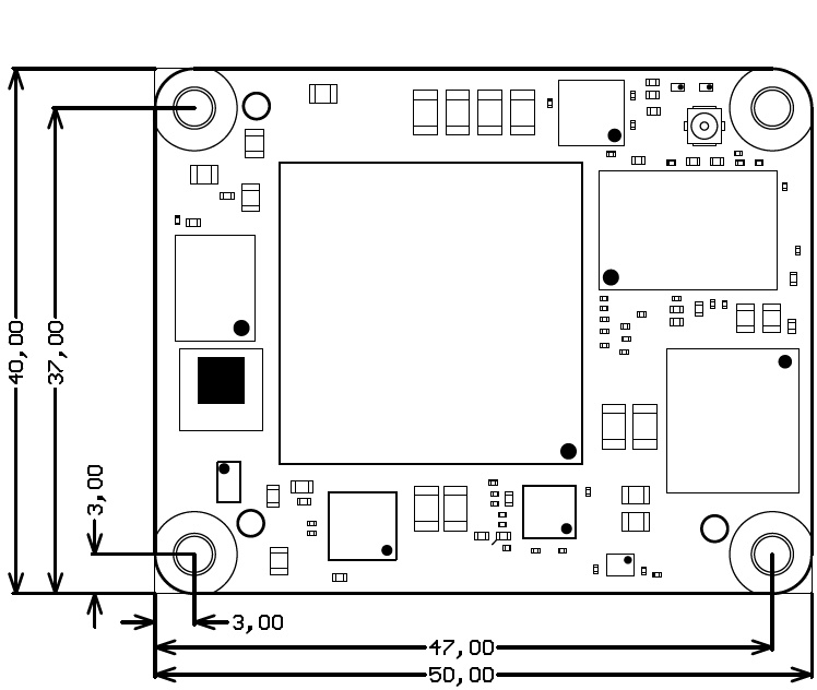
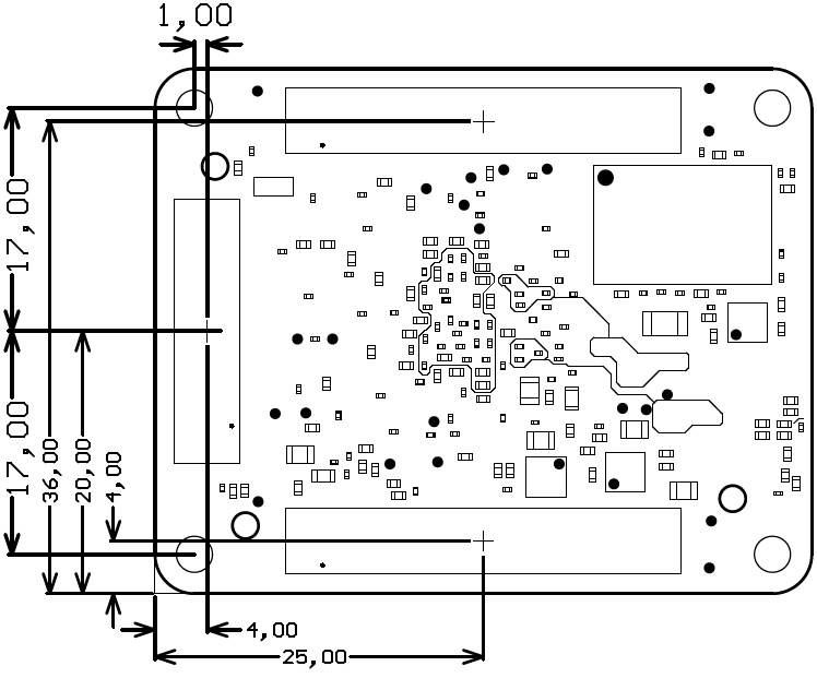
Physical Dimensions
- Module size: 50 mm × 40 mm. Please download the assembly diagram for exact numbers.
- Mating height with standard connectors: 8mm
- PCB thickness: 1.6mm
- Highest part on PCB: approx. 2.5mm. Please download the step model for exact numbers.
All dimensions are shown in millimeters.
Weight
16 - 27 g, Plain module (depends on variant).
8.8 g, Set of nuts and bolts.
Currently Offered Variants
| Trenz shop TE0712 overview page | |
|---|---|
| English page | German page |
Trenz Electronic Shop Overview
Revision History
Hardware Revision History
| Date | Revision | Notes | PCN | Documentation Link |
|---|---|---|---|---|
| 2016-12-09 | 02 | Second production revision | Click to see PCN | TE0712-02 |
| 2013-12-02 | 01 | First production revision | TE0712-01 |
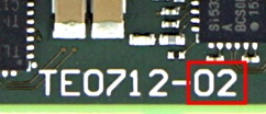
Hardware revision number is printed on the PCB board together with the module model number separated by the dash.
Document Change History
Date | Revision | Contributors | Description |
|---|---|---|---|
Updated Download link for this document | |||
2022-12-22 | v.31 |
| |
| 2020-07-03 | v.23 | John Hartfiel |
|
| 2019-01-10 | v.22 | John Hartfiel |
|
| 2017-12-15 | v.18 | John Hartfiel |
|
| 2017-12-12 | v.15 | John Hartfiel |
|
| 2017-05-29 | v.13 | Jan Kumann |
|
| 2017-03-01 | v.7 | John Hartfiel |
|
| 2017-01-26 | v.3 | Jan Kumann |
|
| 2017-01-20 | v.2 | Jan Kumann |
|
| 2013-12-02 | v.1 | Antti Lukats |
|
| -- | all |
|
Disclaimer
Data Privacy
Please also note our data protection declaration at https://www.trenz-electronic.de/en/Data-protection-Privacy
Document Warranty
The material contained in this document is provided “as is” and is subject to being changed at any time without notice. Trenz Electronic does not warrant the accuracy and completeness of the materials in this document. Further, to the maximum extent permitted by applicable law, Trenz Electronic disclaims all warranties, either express or implied, with regard to this document and any information contained herein, including but not limited to the implied warranties of merchantability, fitness for a particular purpose or non infringement of intellectual property. Trenz Electronic shall not be liable for errors or for incidental or consequential damages in connection with the furnishing, use, or performance of this document or of any information contained herein.
Limitation of Liability
In no event will Trenz Electronic, its suppliers, or other third parties mentioned in this document be liable for any damages whatsoever (including, without limitation, those resulting from lost profits, lost data or business interruption) arising out of the use, inability to use, or the results of use of this document, any documents linked to this document, or the materials or information contained at any or all such documents. If your use of the materials or information from this document results in the need for servicing, repair or correction of equipment or data, you assume all costs thereof.
Copyright Notice
No part of this manual may be reproduced in any form or by any means (including electronic storage and retrieval or translation into a foreign language) without prior agreement and written consent from Trenz Electronic.
Technology Licenses
The hardware / firmware / software described in this document are furnished under a license and may be used /modified / copied only in accordance with the terms of such license.
Environmental Protection
To confront directly with the responsibility toward the environment, the global community and eventually also oneself. Such a resolution should be integral part not only of everybody's life. Also enterprises shall be conscious of their social responsibility and contribute to the preservation of our common living space. That is why Trenz Electronic invests in the protection of our Environment.
REACH, RoHS and WEEE
REACH
Trenz Electronic is a manufacturer and a distributor of electronic products. It is therefore a so called downstream user in the sense of REACH. The products we supply to you are solely non-chemical products (goods). Moreover and under normal and reasonably foreseeable circumstances of application, the goods supplied to you shall not release any substance. For that, Trenz Electronic is obliged to neither register nor to provide safety data sheet. According to present knowledge and to best of our knowledge, no SVHC (Substances of Very High Concern) on the Candidate List are contained in our products. Furthermore, we will immediately and unsolicited inform our customers in compliance with REACH - Article 33 if any substance present in our goods (above a concentration of 0,1 % weight by weight) will be classified as SVHC by the European Chemicals Agency (ECHA).
RoHS
Trenz Electronic GmbH herewith declares that all its products are developed, manufactured and distributed RoHS compliant.
WEEE
Information for users within the European Union in accordance with Directive 2002/96/EC of the European Parliament and of the Council of 27 January 2003 on waste electrical and electronic equipment (WEEE).
Users of electrical and electronic equipment in private households are required not to dispose of waste electrical and electronic equipment as unsorted municipal waste and to collect such waste electrical and electronic equipment separately. By the 13 August 2005, Member States shall have ensured that systems are set up allowing final holders and distributors to return waste electrical and electronic equipment at least free of charge. Member States shall ensure the availability and accessibility of the necessary collection facilities. Separate collection is the precondition to ensure specific treatment and recycling of waste electrical and electronic equipment and is necessary to achieve the chosen level of protection of human health and the environment in the European Union. Consumers have to actively contribute to the success of such collection and the return of waste electrical and electronic equipment. Presence of hazardous substances in electrical and electronic equipment results in potential effects on the environment and human health. The symbol consisting of the crossed-out wheeled bin indicates separate collection for waste electrical and electronic equipment.
Trenz Electronic is registered under WEEE-Reg.-Nr. DE97922676.
Overview
Content Tools