Page History
| HTML |
|---|
<!--
Template Revision 1.4 beta
--> |
| Scroll Ignore |
|---|
| Scroll pdf ignore | |
|---|---|
Table of Contents
|
Overview
| Scroll Only (inline) |
|---|
Refer to https://wiki.trenz-electronic.de/display/PD/ |
...
TE0720+TRM for online version of this manual and additional technical documentation of the product. |
The Trenz Electronic TE0720 is an industrial-grade SoM (System on Module) based on Xilinx Zynq-7000 SoC (XC7Z020 or XC7Z014S) with up to 1 GB of DDR3/L SDRAM, 32MB of SPI flash memory, Gigabit Ethernet PHY transceiver, a USB PHY transceiver and powerful switching-mode power supplies for all on-board voltages. A large number of configurable I/Os is provided via rugged high-speed stacking strips. See also Variants Currently in Production section.
Key Features
- Xilinx XC7Z SoC (XC7Z020 or XC7Z014S)
- Processing system (PS):
- XC7Z020: Dual-core ARM Cortex-A9 MPCore™ with CoreSight™
- XC7Z014S: Single-core ARM Cortex-A9
Unified 512 KByte L2 cache
256 KByte on-chip memory
54 multiplexed I/O pins (MIOs)
- Programmable Logic- MPCore™ with CoreSight™
- L1 cache: 32 KByte instruction, 32 KByte data per processor
- L2 cache: Unified 512 KByte
- Programmable logic (PL): Artix-7 FPGA
- Programmable logic cells
560 KByte extensible block RAM (140x 36 Kbit BRAM blocks)
220 programmable DSP slices
Dual 12-bit 1Msps AD converter
200- : 85K (XC7Z020), 65K (XC7Z014S)
- Block RAM: 4.9 MByte (XC7Z020), 3.8 MByte (XC7Z014S)
- DSP slices: 220 (XC7Z020), 170 (XC7Z014S)
- Peak DSP performance: 276 GMACs (XC7Z020), 187 GMACs (XC7Z014S)
- 2x 12 bit, MSPS ADCs with up to 17 differential inputs
- Processing system (PS):
- 54 multiuse I/O (MIO) pins
- 152 High-Range (HR) I/O pins (SelectIO interfaces)
- System Controller CPLD (Lattice LCMXO2-1200HC)
- Up to 1 GByte DDR3/L SDRAM memory , (2 x 256 Mbit x 16 (, 32-bit wide data bus).
- 32 MByte Quad SPI Flash memory
- Gigabit Ethernet transceiver PHY (Marvell 88E1512)
- MAC address serial EEPROM with EUI-48™ node identity (11AA02E48)
- Highly integrated Highly Integrated full-featured hi-speed USB 2.0 ULPI transceiver (Microchip USB3320C-EZK)
- 3-axis accelerometer and 3-axis magnetometer (ST Microelectronics LSM303DTR) (Not installedOptional!)
- Real time clock with embedded crystal (Intersil ISL12020M): ±5ppm accuracy
- Atmel CryptoAuthentication element (Atmel ATSHA204A)
- Up to 32 GByte eMMC, usually 4 GByte, depends on module variant and assembly option
- User LED 1 (Green), user LED 2 (Red), user LED 3 - FPGA DONE (Green)
- 1.5A, PowerSoC DC-DC step-down converter (Enpirion EP53F8QI) for 1.8V power supply
- 1.5A, PowerSoC DC-DC step-down converter (Enpirion EP53F8QI) for 1.5V power supply
- 4A PowerSoC DC-DC step-down converter (Enpirion EN6347) for 1.0V power supply
- On-board high-efficiency DC-DC converters for all voltages used
- Trenz Trenz 4 x 5 module socket connector connectors (3 x Samtec LSHM series connectors)
- Evenly spread supply pins for good signal integrity
- Rugged for shock and high vibration
Additional assembly options are available for cost or performance optimization upon request.
| Page break |
|---|
Block Diagram
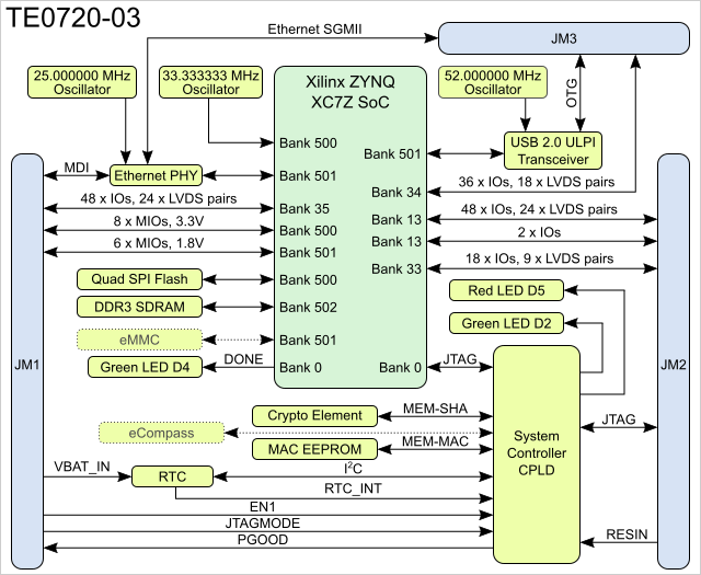
Figure 1: TE0720-03 block diagram.
Components and connections marked with dashed lines are optional or may be missing on some module variants, please contact us for additional information.
Main Components
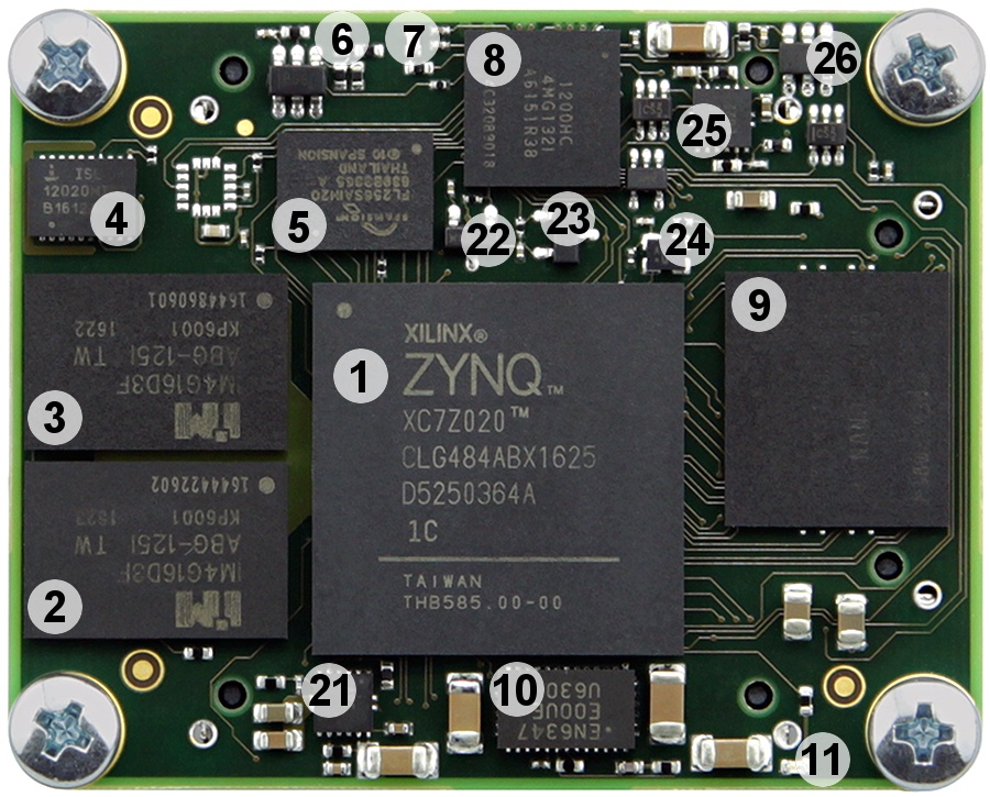
Figure 2: Main components of the module.
- Xilinx Zynq XC7Z SoC, U5
- 4 Gbit DDR3/L SDRAM, U13
- 4 Gbit DDR3/L SDRAM, U12
- Low-power RTC with battery backed SRAM, U20
- 32 MByte Quad SPI Flash memory, U7
- Red LED (LED1LED2), D5
- Green LED (LED2LED1), D2
- System Controller CPLD, U19
- eMMC NAND Flash, U15
- 4A high-efficiency PowerSoC DC-DC step-down Converter converter (1V), U1
- Green LED (DONE), D4
- B2B connector Samtec Razor Beam™ LSHM-130, JM3
- B2B connector Samtec Razor Beam™ LSHM-150, JM1
- B2B connector Samtec Razor Beam™ LSHM-150, JM2
- Hi-speed USB 2.0 ULPI transceiver, U18
- Gigabit Ethernet (GbE) transceiver, U8
- Low-power programmable oscillator @ 52.000000 MHz (OTG-RCLK), U14
- Low-power programmable oscillator @ 33.333333 MHz (PS-CLK), U6
- Low-dropout regulator (VBATT), U24
- DDR termination regulator, U4
- 1.5A PowerSoC DC-DC step-down converter with integrated inductor (1.5V), U2
- Atmel CryptoAuthentication chip, U10
- 2Kbit UNI/O® serial EEPROM with EUI-48™ node identity, U17
- Low-power programmable oscillator @ 25.000000 MHz (ETH-CLK), U9
- 1.5A PowerSoC DC-DC step-down converter with integrated inductor (1.8V), U3
- 3A PFET load switch with configurable slew rate (3.3V), Q1
...
Storage device name | IC | Content | Notes |
|---|---|---|---|
Quad SPI Flash | U7 | Empty | - |
| eMMC NAND Flash | U15 | Empty | - |
| 11AA02E48T EEPROM | U17 | Pre-programmed globally unique, 48-bit node address (MAC) | - |
| System Controller CPLD | U19 | Standard firmware. | Download firmware |
Signals, Interfaces and Pins
Board to Board (B2B) I/Os
I/O signals connected to the SoC's IO bank and B2B connector:
Table 1: Initial state of programmable devices on delivery of the module.
Boot Process
By default the TE-0720 supports QSPI and SD Card boot modes which is controlled by the MODE input signal from the B2B JM1 connector.
MODE Signal State | Boot Mode |
|---|---|
High or open | QSPI |
Low or connected to the ground | SD Card |
Table 14: Boot modes.
Signals, Interfaces and Pins
Board to Board (B2B) I/Os
PL I/O signal connections between Zynq SoC's I/O banks and B2B connectors, 152 HR GPIOs total.
| Bank | Type | Voltage | B2B | I/O Count | Bank | Type | B2B Connector | I/O Signal Count | Voltage | Notes |
|---|---|---|---|---|---|---|---|---|---|---|
| 13 | HR GPIO | VCCIO13 | JM2 | 48 | I/Os, 24 LVDS pairs | VCCIO13 | ||||
| 13 | HR GPIO | VCCIO13 | JM2 | 2 I/Os | VCCIO13 | B13_IO0 and B13_IO25 | ||||
| 33 | HR GPIO | VCCIO33 | JM2 | 18 | I/Os, 9 LVDS pairs | VCCIO33 | ||||
| 34 | HR GPIO | VCCIO34 | JM3 | 36 | I/Os, 18 LVDS pairsVCCIO34 | |||||
| 35 | HR GPIO | VCCIO35 | JM1 | 48 | I/Os, 24 LVDS pairs | VCCIO35 | 500 | MIO | JM1 | 8 MIOs
Table 2: General PL I/O to B2B connectors information.
PS MIO bank 500 and 501 signal connections to B2B JM1 connector, 14 PS MIOs total.
| MIO | B2B Pin | Bank | Voltage | Notes |
|---|---|---|---|---|
| 0 | JM1-87 | 500 | 3.3V |
For detailed information about the pin-out, please refer to the Pin-out tables.
JTAG Interface
JTAG access to the Xilinx Zynq and to the System Controller CPLD is provided through B2B connector JM2.
...
JTAG Signal
...
B2B Connector Pin
...
| Note |
|---|
| JTAGMODE pin 89 in B2B connector JM1 is used to select which device is accessible. Low - Xilinx Zynq, High - System Controller CPLD. |
| Page break |
|---|
System Controller I/O Pins
Special purpose pins are connected to System Controller CPLD and have following default configuration:
...
| 9 | JM1-91 | 500 | 3.3V | |
| 10 | JM1-95 | 500 | 3.3V | |
| 11 | JM1-93 | 500 | 3.3V | |
| 12 | JM1-99 | 500 | 3.3V | |
| 13 | JM1-97 | 500 | 3.3V | |
| 14 | JM1-92 | 500 | 3.3V | Also wired to U19-M4 |
| 15 | JM1-85 | 500 | 3.3V | Also wired to U19-N4 |
| 40 | JM1-27 | 501 | 1.8V | Zynq SoC SD0 |
| 41 | JM1-25 | 501 | 1.8V | Zynq SoC SD0 |
| 42 | JM1-23 | 501 | 1.8V | Zynq SoC SD0 |
| 43 | JM1-21 | 501 | 1.8V | Zynq SoC SD0 |
| 44 | JM1-19 | 501 | 1.8V | Zynq SoC SD0 |
| 45 | JM1-17 | 501 | 1.8V | Zynq SoC SD0 |
Table 3: General PS MIO connections information.
For detailed information about the pin-out, please refer to the Pin-out tables.
JTAG Interface
JTAG access to the Zynq SoC and System Controller CPLD is provided through B2B connector JM2.
JTAG Signal | B2B Connector Pin |
|---|---|
| TMS | JM2-93 |
| TDI | JM2-95 |
| TDO | JM2-97 |
| TCK | JM2-99 |
Table 4: JTAG pins connection.
| Note |
|---|
| JTAGMODE pin 89 in B2B connector JM1 is used to switch access between devices, low selects Zynq SoC, high selects System Controller CPLD. |
System Controller CPLD I/O Pins
Special purpose pins are connected to System Controller CPLD and have following default configuration:
| Pin Name | Mode | Function | Default Configuration |
|---|---|---|---|
| RESIN | Input | Reset input | Active low reset input, default mapping forces POR_B reset to Zynq PS. |
| PGOOD | Output | Power good | Active high when all on-module power supplies are working properly. |
| MODE | Input | Boot mode | Force low for boot from the SD card. Latched at power-on only, not during soft reset! |
| EN1 | Input | Power enable | High enables the DC-DC converters and on-board supplies. Not used if NOSEQ is high. |
| NOSEQ | Input | Power sequencing | Forces the 1.0V and 1.8V DC-DC converters always ON when high. |
| JTAGMODE | Input | JTAG select | Keep low for FPGA JTAG access. |
| MIO7 | Input/Output | GPIO | Connected to System Controller CPLD pin P11, function depends on firmware |
Table 5: System Controller CPLD special purpose pins description.
| Page break |
|---|
Quad SPI Interface
Quad SPI Flash (U7) is connected to the Zynq PS QSPI0 interface via PS MIO bank 500, pins MIO1..6.
| MIO | Signal Name | U7 Pin |
|---|---|---|
| 1 | SPI-CS | C2 |
| 2 | SPI-DQ0/M0 | D3 |
| 3 | SPI-DQ1/M1 | D2 |
| 4 | SPI-DQ2/M2 | C4 |
| 5 | SPI-DQ3/M3 | D4 |
| 6 | SPI-SCK/M4 | B2 |
Table 6: Quad SPI interface MIOs and pins.
eMMC Interface
The TE0720 has on-board eMMC memory device (U15) except TE0720-03-1CR variant. At least three different eMMC devices have been used, please contact Trenz Electronic for more specific information.
| MIO | Signal Name | U15 Pin |
|---|---|---|
| 46 | MMC-D0 | H3 |
| 47 | MMC-CMD | W5 |
| 48 | MMC-CLK | W6 |
| 49 | MMC-D1 | H4 |
| 50 | MMC-D2 | H5 |
| 51 | MMC-D3 | J2 |
Table 7: eMMC interface MIOs and pins.
| Page break |
|---|
Ethernet Interface
The Marvell Alaska 88E1512 (U8) is a physical layer device containing a single Gigabit Ethernet transceiver and three separate major electrical interfaces: MDI interface to copper cable, SERDES/SGMII interface and RGMII interface. RGMII interface is connected to the Zynq SoC PS bank 501 MIO pins, see tables below.
SGMII (SFP copper or fiber) pins are routed to the B2B connector JM3 and MDI pins are routed to the B2B connector JM1 (see table below).
Ethernet PHY to B2B connections
| PHY Signal | B2B Pin | PHY Signal | B2B Pin | |
|---|---|---|---|---|
| SOUT_N | JM3-1 | PHY_MDI1_P | JM1-10 | |
| SOUT_P | JM3-3 | PHY_MDI1_N | JM1-12 | |
| SIN_N | JM3-2 | PHY_MDI2_P | JM1-16 | |
| SIN_P | JM3-4 | PHY_MDI2_N | JM1-18 | |
| PHY_MDI0_P | JM1-4 | PHY_MDI3_P | JM1-22 | |
| PHY_MDI0_N | JM1-6 | PHY_MDI3_N | JM1-24 |
Table 8: Ethernet PHY to B2B connections.
Ethernet PHY to Zynq SoC PS MIO ETH0 connections
| PHY Signal | SoC MIO | PHY Signal | SoC MIO | |
|---|---|---|---|---|
| ETH-TXCK | 16 | ETH-RXCK | 22 | |
| ETH-TXD0 | 17 | ETH-RXD0 | 23 | |
| ETH-TXD1 | 18 | ETH-RXD1 | 24 | |
| ETH-TXD2 | 19 | ETH-RXD2 | 25 | |
| ETH-TXD3 | 20 | ETH-RXD3 | 26 | |
| ETH-TXCTL | 21 | ETH-RXCTL | 27 | |
| ETH-MDC | 52 | ETH-MDIO | 53 |
Table 9: Ethernet PHY to Zynq SoC connections.
| Page break |
|---|
USB Interface
Hi-speed USB ULPI PHY is provided by USB3320 from Microchip (U18). The ULPI interface is connected to the Zynq SoC PS USB0 via MIO28..39, bank 501.
| USB PHY Signal | Wired to | SoC MIO |
|---|---|---|
| OTG-DATA4 | U18-7 | 28 |
| OTG-DIR | U18-31 | 29 |
| OTG-STP | U18-29 | 30 |
| OTG-NXT | U18-2 | 31 |
| OTG-DATA0 | U18-3 | 32 |
| OTG-DATA1 | U18-4 | 33 |
| OTG-DATA2 | U18-5 | 34 |
| OTG-DATA3 | U18-6 | 35 |
| OTG-CLK | U18-1 | 36 |
| OTG-DATA5 | U18-9 | 37 |
| OTG-DATA6 | U18-10 | 38 |
| OTG-DATA7 | U18-13 | 39 |
Table 10: USB ULPI PHY to Zynq SoC connections.
USB PHY connection
| USB PHY Pin | SC CPLD Pin | B2B Name | Notes |
|---|---|---|---|
| REFSEL0..2 | - | - | Reference clock frequency select, all set to GND = 52.000000 MHz. |
| RESETB | B14, bank 1 | - | Active low reset. |
| CLKOUT | - | - | ULPI output clock connected to Zynq PS MIO36. |
| DP, DM | OTG-D_P, OTG-D_N | USB data lines. | |
| CPEN | VBUS_V_EN | External USB power switch active high enable signal. | |
| VBUS | - | USB-VBUS | Connect to USB VBUS via a series of resistors, see reference schematic. |
| ID | - | OTG-ID | For A-device connect to the ground, for B-device leave floating. |
| SPK_L | M5, bank 2 | - | In USB audio mode a switch connects the DM pin to the SPK_L. |
| SPK_R | M8, bank 2 | - | In USB audio mode a switch connects the DP pin to the SPK_R. |
Table 11: USB ULPI PHY connections.
I2C Interface
On-board I2C devices are connected to the System Controller CPLD which acts as a I2C bus repeater for the Zynq SoC. System Controller CPLD signals X1, X3 and X7 are routed to Zynq SoC bank 34. Exact functionality depends on the System Controller CPLD firmware.
| Signal Name | SC CPLD Pin | SoC Pin | Notes |
|---|---|---|---|
| X1 | F1 | L16 | SCL, I2C clock. |
| X5 | J1 | P22 | SDA, I2C data out. |
| X7 | M1 | N22 | SDA, I2C data in. |
Table 12: Zynq SoC to System Controller CPLD I2C bus.
| I2C Device | I2C Address | IC | Notes |
|---|---|---|---|
| ISL12020M RTC | 0x6F | U20 | RTC registers. |
| ISL12020M SRAM | 0x57 | U20 | Battery backed RAM in RTC IC. |
| LSM303D | 0x1D | U22 | Optional, not soldered on current production variants. |
Table 13: I2C slave device addresses.
On-board Peripherals
System Controller CPLD
The System Controller CPLD (U19) is provided by Lattice Semiconductor LCMXO2-1200HC (MachXO2 product family). The System Controller CPLD is the central system management unit where essential control signals are logically linked by the implemented logic in System Controller CPLD firmware, which generates output signals to control the system, the on-board peripherals and the interfaces. Also interfaces like JTAG and I2C between the on-board peripherals and to the Zynq SoC are by-passed, forwarded and controlled.
Other tasks of the System Controller CPLD are monitoring of the power-on sequence and to indicate the programming state of the Zynq SoC FPGA.
For more detailed information, refer to the TE0720 System Controller CPLD firmware page.
DDR Memory
By default TE0720 module has two DDR3/L SDRAM chips arranged into 32-bit wide memory bus providing total on-board memory size up to 1 GBytes. Size of memory depends on the module variant, refer to the variants table.
Quad SPI Flash Memory
On-board 32-MByte QSPI flash memory S25FL256S (U7) is used to store initial FPGA configuration. Besides FPGA configuration, remaining free flash memory can be used for user application and data storage. All four SPI data lines are connected to the FPGA allowing x1, x2 or x4 data bus widths. Maximum data rate depends on the selected bus width and clock frequency used.
| Note |
|---|
SPI Flash QE (Quad Enable) bit must be set to high or FPGA is unable to load its configuration from flash during power-on. By default this bit is set to high at the manufacturing plant. |
eMMC Flash Memory
eMMC Flash memory device(U15) is connected to the Zynq PS MIO bank 501 pins MIO46..MIO51 (see also Variants Currently in Production for options). Depending on the module variant, different make and model of eMMC chips are available.
Gigabit Ethernet PHY
On-board Gigabit Ethernet PHY is provided with Marvell Alaska 88E1512 IC (U8). The Ethernet PHY RGMII interface is connected to the Zynq Ethernet0 PS GEM0. I/O voltage is fixed at 1.8V for HSTL signalling. The reference clock input of the PHY is supplied from an on-board 25.000000 MHz oscillator (U9), the 125MHz output clock signal CLK_125MHZ is connected to the pin G13 of the System Controller CPLD chip (U19).
| PHY Signal | SC CPLD Pin |
|---|---|
| ETH-MDC | L14 |
| ETH-MDIO | K14 |
| PHY_LED0 | F14 |
| PHY_LED1 | D12 |
| PHY_LED2 | C13 |
| PHY_CONFIG | C14 |
| ETH-RST | E14 |
| CLK_125MHZ | G13 |
Table 15: Ethernet PHY to SC CPLD connections.
| Page break |
|---|
High-speed USB ULPI PHY
Hi-speed USB ULPI PHY is provided with USB3320 from Microchip. The ULPI interface is connected to the Zynq PS USB0 via MIO28..39, bank 501 (see also section. The I/O voltage is fixed at 1.8V and PHY reference clock input is supplied from the on-board 52.000000 MHz oscillator (U14).
RTC - Real Time Clock
Temperature compensated Intersil ISL12020M IC is used for Real Time Clock (U20). Battery voltage must be supplied to the module VBAT_IN pin from the carrier board to use battery backed functionality. Battery backed registers can be accessed over I2C bus at slave address of 0x6F. General purpose RAM is at I2C slave address 0x57. RTC IC is supported by Linux so it can be used as hwclock device.
MAC-Address EEPROM
A Microchip 2Kbit 11AA02E48 serial EEPROM (U17) is connected to the System Controller CPLD pin M14 via single-I/O UNI/O serial interface and contains pre-programmed globally unique 48-bit node address compatible with EUI-48TM specification. Chip is programmed at the factory with a globally unique node address stored in the upper 1/4 of the memory array and write-protected through the STATUS register. The remaining 1,536 bits are available for application use.
Atmel CryptoAuthentication Chip
The ATSHA204A Atmel CryptoAuthenticationTM chip (U10) is connected to the System Controller CPLD pin N14 via single-wire interface providing various security functions and features such as anti-counterfeiting, firmware/media protection, password validation, secure session key exchanging, secure data storage and more. Refer to the product datasheet for more information.
eCompass module
Optionally TE0720 module can be fitted with ultra-compact high-performance eCompass device (LSM303D, U22) featuring 3D accelerometer and 3D magnetometer.
Oscillators
| Source | Signal | Frequency | Destination | Pin Name | Notes |
|---|---|---|---|---|---|
| U6 | PS-CLK | 33.333333 MHz | U5 | PS_CLK_500 | Zynq SoC PS subsystem main clock. |
| U14 | OTG-RCLK | 52.000000 MHz | U18 | REFCLK | USB3320C PHY reference clock. |
| U9 | ETH-CLK | 25.000000 MHz | U8 | XTAL_IN | 88E1512 PHY reference clock. |
Table 16: Oscillators.
On-board LEDs
| LED | Color | Connected to | Description and Notes |
|---|---|---|---|
| D2 | Green | LED1 | Controlled by System Controller CPLD firmware. |
| D4 | Green | DONE | |
| D5 | Red | LED2 | Controlled by System Controller CPLD firmware. |
Table 17: On-board LEDs
On-board LEDs
...
Clocking
...
PS-CLK
...
33.333333 MHz
...
U6
...
PS_CLK_500
...
PS subsystem main clock.
...
OTG-RCLK
...
52.000000 MHz
...
-
...
USB3320C reference clock.
...
| Page break |
|---|
Default MIO Mapping
...
| Page break |
|---|
Gigabit Ethernet
On-board Gigabit Ethernet PHY is provided with Marvell Alaska 88E1512 IC (U8). The Ethernet PHY RGMII interface is connected to the Zynq Ethernet0 PS GEM0. I/O voltage is fixed at 1.8V for HSTL signalling. SGMII (SFP copper or fiber) can be used directly with the Ethernet PHY, as the SGMII pins are available on the B2B connector JM3. The reference clock input of the PHY is supplied from an on-board 25.000000 MHz oscillator (U9), the 125MHz output clock signal CLK_125MHZ is connected to the pin G13 of the System Controller CPLD chip (U19).
Ethernet PHY connection
...
| Page break |
|---|
USB Interface
USB PHY is provided by USB3320 from Microchip. The ULPI interface is connected to the Zynq PS USB0 via MIO28..39, bank 501. The I/O voltage is fixed at 1.8V and reference clock input of the PHY is supplied from the on-board 52.000000 MHz oscillator (U14).
USB PHY connection
...
The schematics for the USB connector and required components is different depending on the USB usage. USB standard A or B connectors can be used for host or device modes. A mini-USB connector can be used for USB device mode. A micro-USB connector can be used for device mode, OTG mode or host mode.
I2C Interface
On-board I2C devices are connected to the System Controller CPLD, device slave addresses are listed in the table below:
...
Boot Process
By default the TE-0720 supports QSPI and SD Card boot modes which is controlled by the MODE input signal from the B2B JM1 connector.
...
MODE Signal State
...
High or open
...
SD Card
...
Low or connected to the ground
...
QSPI
On-board Peripherals
32 MByte Quad SPI Flash Memory
On-board QSPI flash memory S25FL256S (U7) is used to store initial FPGA configuration. Besides FPGA configuration, remaining free flash memory can be used for user application and data storage. All four SPI data lines are connected to the FPGA allowing x1, x2 or x4 data bus widths. Maximum data rate depends on the selected bus width and clock frequency used.
| Note |
|---|
SPI Flash QE (Quad Enable) bit must be set to high or FPGA is unable to load its configuration from flash during power-on. By default this bit is set to high at the manufacturing plant. |
Processing System (PS) Peripherals
...
MIO16..27
MIO52..53
...
1) Different make and model may be installed on different module variants.
RTC - Real Time Clock
Temperature compensated Intersil ISL12020M IC is used for Real Time Clock (U20). Battery voltage must be supplied to the module VBAT_IN pin from the carrier board to use battery backed functionality. Battery backed registers can be accessed over I2C bus at slave address of 0x6F. General purpose RAM is at I2C slave address 0x57. RTC IC is supported by Linux so it can be used as hwclock device.
MAC-Address EEPROM
A Microchip 2Kbit 11AA02E48 serial EEPROM (U17) is connected to the System Controller CPLD and contains globally unique 48-bit node address which is compatible with EUI-48TM specification. Upper 1/4 of the memory array contains 48-bit node address and is write protected.
Power and Power-On Sequence
...
| Power Input Pin | Typical Current |
|---|---|
| VIN | TBD* |
| 3.3VIN | TBD* |
Table 18: Power Consumption.
* TBD - To Be Determined soon with reference design setup.
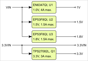
Power Distribution Diagram
.
Power Distribution Diagram
Figure 3: Power distribution diagram.
| Note |
|---|
Current rating of Samtec Razor Beam™ LSHM B2B connectors is 2.0A per pin (2 adjacent pins powered). |
| Page break |
|---|
Power-On Sequence
For highest efficiency of the on-board DC-DC regulators, it is recommended to use same single 3.3V power source for both VIN and 3.3VIN power rails. Although VIN and 3.3VIN can be powered up in any order, it is recommended to power them up simultaneously.
It is important that all carrier board I/Os are 3-stated at power-on until System Controller CPLD sets PGOOD signal high (B2B connector JM1, pin 30), or 3.3V is present on B2B connector JM2 pins 10 and 12, meaning that all on-module voltages have become stable and module is properly powered up.
Use 3.3V or 1.8V output to enable external power supplies or power switches which are used to supply FPGA banks.
See also Xilinx datasheet DS187 for additional information. User should also check related carrier board documentation when choosing carrier board design for TE0720 module.
...
NOSEQ input signal from the carrier board can be used to control output of the two DC-DC converters U1 and U3. It works in conjunction with the System Controller CPLD firmware controlled ON_1V0 and ON_1V8 input signals of the U21 and U25 gate ICs.
|
|
| If NOSEQ input signal from the carrier board is low (logical 0), signals ON_1V0 and ON_1V8 can be driven by System Controller CPLD to control outputs of the U1 and U3 DC-DC converters. | If NOSEQ input signal from the carrier board is high (logical 1), state of the ON_1V0 and ON_1V8 signals is irrelevant and DC-DC converters U1 and U3 outputs are always enabled. |
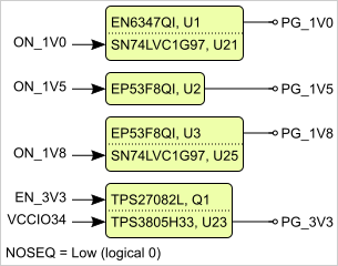
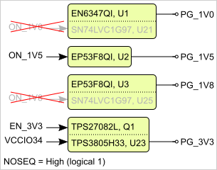
Figure 4: Power sequencing.
| Note |
|---|
Initial state of the ON_1V0 and ON_1V8 signals and therefore also functionality of the NOSEQ signal depend on the System Controller CPLD firmware. |
| Page break |
|---|
Power Rails
B2B Name | B2B JM1 Pins | B2B JM2 Pins | Direction | Note |
|---|---|---|---|---|
| VIN | 1, 3, 5 | 2, 4, 6, 8 | Input | Supply voltage from carrier board. |
| 3.3VIN | 13, 15 | 91- | Input | Supply voltage from carrier board. JM2-91 is VREF_JTAG.. |
| JTAG VREF | - | 91 | Output | JTAG reference voltage. Attention: Net name on schematic is "3.3VIN" |
| VCCIO35 | 9, 11 | - | Input | High range bank voltage from carrier board. |
| VCCIO33 | - | 5 | Input | High range bank voltage from carrier board. |
| VCCIO13 | - | 7, 9 | Input | High range bank voltage from carrier board. |
| VCCIO34 | - | 1, 3 | Input | High range bank voltage from carrier board. |
| VBAT_IN | 79 | - | Input | RTC battery-buffer supply voltage. |
| 3.3V | - | 10, 12 | Output | Internal 3.3V voltage level. |
| 1.8V | 39 | - | Output | Internal 1.8V voltage level. |
| 1.5V 1) | - | 19 | Output | Internal 1.5V voltage level. |
Table 19: Module power rails.
1) In case of module variant of TE0720-03-L1IF which uses Xilinx Zynq XC7Z020-L1CLG484I chip with lower power consumption, power rails named 1.5V and VCCO_DDR_502 voltage is actually 1.35V. To achieve this, a resistor with different value is used for R4 (see schematics schematic of the TE0720-03-L1IF for more information).
Bank Voltages
Bank | Schematics Schematic Name | Voltage | Notes | ||
|---|---|---|---|---|---|
| 500 | 3.3V, VCCO_MIO0_500 | 3.3V | |||
| 501 | 1.8V, VCCO_MIO1_501 | 1.8V | |||
| 502 | 1.5V, VCCO_DDR_502 | 1.5V | |||
| 0 Config | 3.3V | 3.3V | |||
| 1.8V | |||||
| 502 | 1.5V, VCCO_DDR_502 | 1.5V | |||
| 0 Config | 3.3V | 3.3V | |||
| 13 HR | VCCO13 | 1.2V to 3.3V | Supplied by the carrier board. | ||
| 33 HR | VCCIO33 | 1.2V to 3.3V | Supplied by the carrier board. | ||
| 34 HR | VCCIO34 | 1.25V to 3.3V | Supplied by the carrier board. | ||
| 35 HR | VCCIO35 | 13 HR | VCCO13 | 1.2V to 3.3V | Supplied by the carrier board. |
| 33 HR | VCCIO33 | 1.2V to 3.3V | Supplied by the carrier board. | ||
| 34 HR | VCCIO34 | 1.2V to 3.3V | Supplied by the carrier board. | ||
| 35 HR | VCCIO35 | 1.2V to 3.3V | Supplied by the carrier board. |
Board to Board Connectors
...
Variants Currently in Production
...
RAM
...
eMMC
Size
...
Temperature
Range
...
B2B Connector
Height
...
Table 20: Zynq SoC bank voltages.
Board to Board Connectors
| Include Page | ||||
|---|---|---|---|---|
|
Variants Currently in Production
| Page properties | ||||
|---|---|---|---|---|
| ||||
| Note: Only table was changed, chapter must be updated in case of TRM Style update |
| Trenz shop TE0720 overview page | |
|---|---|
| English page | German page |
Table 21: Module variants currently in production.
Technical Specifications
Absolute Maximum Ratings
Parameter | Min | Max | Units | Reference Document |
|---|---|---|---|---|
VIN supply voltage | -0.3 | 6.5 | V | EP53F8QI datasheet. |
| 3.3VIN supply voltage | -0.1 | 3.75 | V | TPS27082L and LCMXO2-1200HC datasheets. |
| Supply voltage for PS MIO banks | -0.5 | 3.6 | V | See Xilinx DS187 datasheet. |
| I/O input voltage for MIO banks | -0.4 | VCCO_MIO + 0.55 | V | See Xilinx DS187 datasheet. (VCCO_MIO0_500, VCCO_MIO1_501) |
| Supply voltage for HR I/Os banks | -0.5 | 3.6 | V | See Xilinx DS187 datasheet. (VCCIO13, VCCIO33, VCCIO34, VCCIO35) |
| I/O input voltage for HR I/O banks | -0.4 | VCCIO + 0.55 | V | See Xilinx DS187 datasheet. |
Storage temperature | -40 | +85 | °C | - |
| Storage temperature without the ISL12020MIRZ, eMMC Flash and 88E1512 PHY installed | -55 | +100 | °C | NB! Module variants using Nanya SDRAM chips, max temperature limit is +125 °C. |
Table 22: Module absolute maximum ratings.
| Note |
|---|
| Assembly variants for higher storage temperature range are available on request. |
| Note |
|---|
| Please check Xilinx datasheet DS187 for complete list of absolute maximum and recommended operating ratings. |
Recommended Operating Conditions
Technical Specifications
Absolute Maximum Ratings
| Parameter | Min | Max | Units | Reference Document |
|---|---|---|---|---|
| VIN supply voltage |
| 2. |
| 5 |
| 5.5 | V | EN6347QI and EP53F8QI |
| datasheets. |
| 3.3VIN supply voltage |
| 3. |
| 135 | 3. |
| 465 | V |
| 3.3V +/- 5%. |
| Supply voltage for PS MIO banks |
| 1. |
| 71 | 3. |
| 465 | V | See Xilinx DS187 datasheet. |
| I/O input voltage for PS MIO banks | -0. |
| 20 | VCCO_MIO + 0. |
| 20 | V | See Xilinx DS187 |
| datasheet. |
| Supply voltage for HR I/Os banks |
| 1. |
| 14 | 3. |
| 465 | V | See Xilinx DS187 datasheet. |
(VCCIO13, VCCIO33, VCCIO34, VCCIO35)
| I/O input voltage for HR I/O banks | -0. |
| 20 | VCCIO + 0. |
| 20 | V | See Xilinx DS187 datasheet. |
Storage temperature
-40
+85
°C
| Note |
|---|
| Assembly variants for higher storage temperature range are available on request. |
| Note |
|---|
| Please check Xilinx datasheet DS187 for complete list of absolute maximum and recommended operating ratings. |
Recommended Operating Conditions
...
Table 23: Recommended operating conditions.
Operating Temperature Ranges
Commercial grade: 0°C to +70°C.
Industrial and automotive grade: -40°C to +85°C.
Operating temperature range depends also on customer design and cooling solution. Please contact us for options.
Physical Dimensions
Module size: 50 mm × 40 mm. Please download the assembly diagram for exact numbers.
Mating height with standard connectors: 8 mm.
PCB thickness: 1.6 mm.
Highest part on PCB: approx. 2.5 mm. Please download the step model for exact numbers.
All dimensions are given in millimeters.
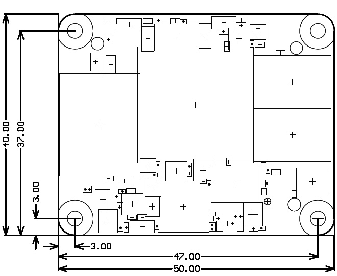
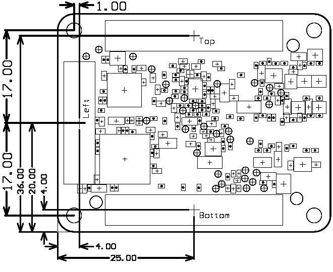
Figure 5: TE0720 module physical dimensions.
Revision History
Hardware Revision History
Table 24: Hardware revision history table.
There is no hardware revision number marking on the module PCB.
Document Change History
Date | Revision | Contributors | Description | ||||||||||||||||||||||
|---|---|---|---|---|---|---|---|---|---|---|---|---|---|---|---|---|---|---|---|---|---|---|---|---|---|
|
|
|
| ||||||||||||||||||||||
| 2021-06-21 | v.93 | Mohsen Chamanbaz |
| ||||||||||||||||||||||
| 2019-02-05 | v.92 | John Hartfiel |
| ||||||||||||||||||||||
2018-07-05 | v.89 | John Hartfiel |
| ||||||||||||||||||||||
| 2017-11-10 | v.85 | John Hartfiel |
| ||||||||||||||||||||||
| 2017-09-07 | v.84 | John Hartfiel |
| ||||||||||||||||||||||
| 2017-08-31 | v.83 | Jan Kumann |
| ||||||||||||||||||||||
-- | all |
|
|
Table 25: Document change history table
Operating Temperature Ranges
Commercial grade: 0°C to +70°C.
Industrial and automotive grade: -40°C to +85°C.
Operating temperature range depends also on customer design and cooling solution. Please contact us for options.
Physical Dimensions
Module size: 50 mm × 40 mm. Please download the assembly diagram for exact numbers.
Mating height with standard connectors: 8 mm.
PCB thickness: 1.6 mm.
Highest part on PCB: approx. 2.5 mm. Please download the step model for exact numbers.
All dimensions are given in millimeters.
Weight
ca 23 g - Plain module
Revision History
Hardware Revision History
...
Notes
...
01
...
Prototypes
...
Hardware revision number is printed on the PCB board together with the module model number separated by the dash.
Put pic of PCB silk screen here showing model and revision ...
Document Change History
...
Date
...
Revision
...
Contributors
...
Description
...
Jan Kumann
...
.
Disclaimer
| Include Page | ||||
|---|---|---|---|---|
|
Overview
Content Tools