Page History
...
| Bank | Type | Connector | I/O Signal Count | Voltage | Notes |
|---|---|---|---|---|---|
| 34 | HR | J1 | 8 | 3.3V | Signal Schematic names: 'SCL', 'SDA', 'D8' ... 'D13'. |
| 34 | HR | J2 | 8 | 3.3V | Signal Schematic names: 'RXD', 'TXD', 'D2' ... 'D7'. |
| 34 | HR | J6 | 8 | 3.3V | Signal Schematic names: 'PIO01' ... 'PIO08'. |
| 34 | HR | J11 | 1 | 3.3V | Signal Schematic name: 'AIN_FPGA'. |
| 35 | HR | J4 | 6 | 3.3V | Signal Schematic names: 'AIN0' ... 'AIN5', usable as single ended of differential analog input inputs or regular digital I/O's. |
| 35 | HR | J5 | 1 | 3.3V | Connector dedicated to ESP8266 module. |
| 500 | MIO | J10 | 7 | 3.3V | SDIO interface to SD Card socket. |
| 501 | MIO | J5 | 4 | 3.3V | Connector dedicated to ESP8266 module . |
Table 2: Overview of the Zynq SoC's PS/PL banks I/O signals
...
| Bank | Type | VCCIO | I/O Signal Count | Available on Connectors | Notes |
|---|---|---|---|---|---|
| 34 | HR | 3.3V | 44 | 25 | 8 user I/O's on Pmod connector J6, female pin header J1 and J2 each. 1 I/O on pin header J11. |
| 35 | HR | 3.3V | 8 | 7 | 6 user I/O's on female pin header J4, 1 user I/O on female pin header J5. |
| 500 | PS MIO | 3.3V | 15 | - | 6 MIO pins used for QSPI flash memory interface, 7 MIO pins used for SD Card interface, 1 MIO pin connected to red LED D2, 1 MIO pin as reset pin routed to USB PHY U18, 'POR_B'-signal is connected to voltage monitor circuit 23. |
| 501 | PS MIO | 3.3V | 16 | 4 | 12 MIO pins used for USB ULPI interface, 4 MIO pins used for ESP8266 interface header J5. |
| 0 | Config | 3.3V | 54 | - | 4 I/O's are dedicated to JTAG interface, 'PROG_B'-signal is connected to voltage monitor circuit 23. |
Table 3: General overview of Zynq SoC PL/PS I/O bank
...
| Analog differential Input Pin Pair | Connector pin | Connector pinSignal Schematic Name | Note |
|---|---|---|---|
| IO_L1P_T0_AD0P_35, pin F12 IO_L1N_T0_AD0N_35, pin E13 | J4-3 J4-1 | AIN2 AIN0 | I/O's also usable in digital mode |
IO_L2P_T0_AD8P_35, pin F11 | J4-4 J4-2 | AIN3 AIN1 | I/O's also usable in digital mode |
IO_L3P_T0_DQS_AD1P_35, pin F13 | J4-6 J4-5 | AIN5 AIN4 | I/O's also usable in digital mode |
Table 12: Auxiliary Analog Inputs of the Zynq device
Note: These 6 auxiliary analog inputs pins are analog inputs are shared with PL bank pins and can be used as regular digital I/O's.
...
The TE0723 board is equipped with one push buttons S1:
| Button | Signal Schematic Name | Connected to | Notes |
|---|---|---|---|
| S1 |
| NRST |
| Voltage Monitor Circuit, U23 | Triggers system reset. |
Table 15: Push buttons of the module
...
Power consumption is to be determined by the user and depends on SoC's FPGA design and connected hardware.
| Board Variant | FPGA | Design | Typical Power, 25°C ambient |
|---|---|---|---|
| TE0723-02 | XC7Z010-1CLG225C | Not configured | TBD* |
| TE0723-03M | XC7Z010-1CLG225C | Not configured | TBD* |
| TE0723-03-07S-1C | XC7Z007S-1CLG225C | Not configured | TBD* |
Table 1516: Module power consumption
...
The voltage direction of the power rails is directed at on-board connectors' view:
Header
J6
VCCIO_33
2, 4, 6 -
.8V
Out 5 - 2.5V Out 3 -
1 - J7 VCCIO_13
In
, 6
1.8V
2.5V OUt 3 - 3.3V Out 1 -
| Main Power Pins Designator | VCC / VCCIO | Direction | Pins | Notes |
|---|
| J12 |
| 5V | In |
1 |
| 5V power supply pin header. | |
| J3 | 3 |
| .3V | Out |
| 2, 4 |
| On- |
| board 3.3V voltage level available. | |
| 5V | In / |
| Out | 5 | On- |
Table 20: Power Pin description of VCCIO selection jumper pin header.
| board 5.0V voltage level available or supply pin. |
Table 17: Main power pin header description
| I/O pin header |
|---|
| VCC / VCCIO | Direction | Pins | Notes |
|---|
| J5 |
| 3.3V |
| Out |
1
4, 8 | I/O header VCCIO. | |||
| J6 | 3.3V | Out | 6, 12 | I/O header VCCIO. |
Table 21: Main Power jack and pins description.Table 18: Power pin description of I/O pin header
| Peripheral Socket Designator | VCC / VCCIO | Direction | Pins | Notes |
|---|
| J8 / |
| J9 | USB-VBUS | In / Out | 1 | Direction depends on USB2 mode. |
| J10 |
| 3.3V | Out | 4 | MikroSD Card socket VDD. |
Table 2219: Power pin description of peripheral connector.
...
Power Rail Name
...
J3 Pins
...
Direction
...
Bank Voltages
...
Table 16: Board power rails
Bank Voltages
Bank
Bank I/O Voltage VCCO
Voltage Range
Bank | Bank I/O Voltage VCCO | Voltage Range |
|---|---|---|
| 0 (config) | 3.3V | fixed |
| 500 (MIO) | 3.3V | fixed |
| 501 (MIO) | 3.3V | fixed |
| 34 (HR) | 3.3V | fixed |
| 35 (HR) | 3.3V | fixed |
Table 1720: Board bank voltages
Variants Currently in Production
| Board Variant | Xilinx Zynq SoC | DDR3L SDRAM | ARM Cores | PL Cells | LUTs | Flip-Flops | Block RAM | DSP Slices | Zynq SoC Operating Temp. | Temp. Range |
|---|---|---|---|---|---|---|---|---|---|---|
| TE0723-TE0723-02 | XC7Z010-1CLG225C | 128 MBytes | Dual-core | 28K | 17,6K | 35,2K | 2.1 MBytes | 80 | 0°C to +85°C | Commercial |
| TE0723-03M | XC7Z010-1CLG225C | 512 MBytes | Dual-core | 28K | 17,6K | 35,2K | 2.1 MBytes | 80 | 0°C to +85°C | Commercial |
| TE0723-03-07S-1C | XC7Z007S-1CLG225C | 512 MBytes | Single-core | 23K | 14,4K | 28,8K | 1.8 MBytes | 66 | 0°C to +85°C | Commercial |
Table 1821: Board variants
Technical Specifications
Absolute Maximum
...
Rating
Parameter | Min | Max | Units | Reference Document |
|---|
VIN supply voltage
V
Storage temperature
-40
+85
°C
Table 19: Board absolute maximum ratings.
Recommended Operating Conditions
...
5V power supply voltage | 4.75 | 5.25 | V | USB2.0 VBUS voltage specification |
| HR PL I/O banks input voltage (VCCIO single ended) | -0.4 | VCCO + 0.55 | V | Xilinx datasheet DS187 (VCCO 3.3V nominal) |
| PS MIO I/O banks input voltage (VCCIO single ended) | -0.4 | VCCO + 0.55 | V | Xilinx datasheet DS187 (VCCO 3.3V nominal) |
| Analog Multiplexer IC pins input voltage | 0 | 3.3V | V | TI CDx4HC405x data sheet |
Storage temperature | -40 | +85 | °C | WL-SMCW SMD LED data sheet |
Table 22: Board absolute maximum ratings
Recommended Operating Conditions
| Parameter | Min | Max | Units | Reference Document |
|---|---|---|---|---|
| 5V power supply voltage | 4.75 | 5.25 | V | USB2.0 VBUS voltage specification |
| HR PL I/O banks input voltage (VCCIO single ended) | -0.20 | VCCO + 0.20 | V | Xilinx datasheet DS187 (VCCO 3.3V nominal) |
| PS MIO I/O banks input voltage (VCCIO single ended) | -0.20 | VCCO + 0.20 | V | Xilinx datasheet DS187 (VCCO 3.3V nominal) |
| Analog Multiplexer IC pins input voltage | 0 | 3.3V | V | TI CDx4HC405x data sheet |
Operating Temperature Commercial | 0 | +85 | °C | Xilinx datasheet DS190 |
Table 23: Board recommended operating conditions
...
| Note |
|---|
| Please check Xilinx datasheet DS187 for complete list of absolute maximum and recommended operating ratings for the Zynq-7 device. |
...
Please note that two different units are used on the figures below, SI system millimeters (mm) and imperial system thousandths of an inch(mil). To convert mils to millimeters and vice versa use formula 100mil's = 2,54mm.
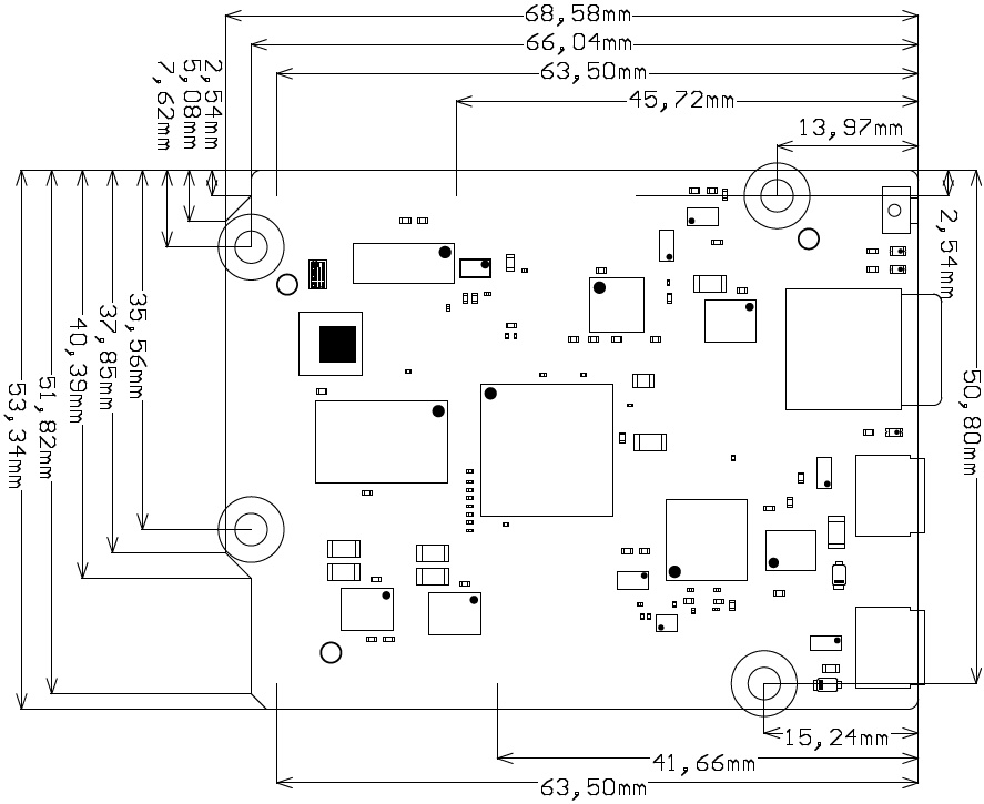
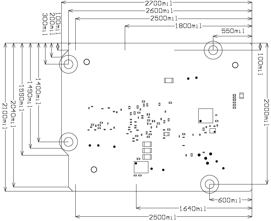
Figure 5: Board physical dimensions
...
| Date | Revision | Notes | PCN | Documentation Link |
|---|---|---|---|---|
| 2016-07-15 | 03 | Refer to Changes list in Schematic for further details in changes to REV02 | - | TE0723-03 |
2015-11-06 | 02 | Second Production Release | - | TE0723-02 |
| - | 01 | First Production Release | - | - |
Table 2124: Board hardware revision history
...
Figure 6: TE0723 board hardware revision number
Document Change History
Date | Revision | Contributors | Description | ||||||||
|---|---|---|---|---|---|---|---|---|---|---|---|
| Ali Naseri, |
|
Table 2225: Document change history.
...
Overview
Content Tools