Page History
...
| HTML |
|---|
<!-- Template Revision 1.63 (HTML comment will not display, it's not needed to remove them. For Template/Skeleton changes, increase Template Revision number. So we can check faster, if the TRM style is up to date) --> |
| scroll-ignore | |
|---|---|
| scroll-pdf-ignore | |
Table of Contents
|
Overview
| Scroll Only (inline) |
|---|
Refer to https://wiki.trenz-electronic.de/display/ |
...
PD/TE0722+TRM for downloadable version of this manual and additional technical documentation of the product. |
The Trenz Electronic TE0722-02 is a DIPFORTy1 "Soft Propeller" based on the Xilinx Zynq-7000 SoC.
...
- Xilinx Zynq XC7Z010 SoC
- Dual-core ARM A9+ (TE0722-02-07S-1C variant has single-core ARM A9+)
- 16 MByte quad Quad SPI Flash
- Micro SD Card socket with card detect signal
- 34 I/Os on DIP40 header pins
- System status LED (DONE)
- RGB LED connected to PL I/O
- Green user LED connected to ARM CPU GPIO
- Proximity and ambient light sensor
- DIP40 form factor (size 18 x 51 mm)
Additional assembly options are available for cost or performance optimization upon request.
Block Diagram
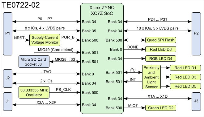
Figure 1: TE022-02 block diagram.
Main Components
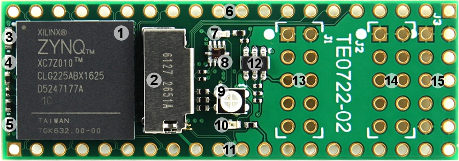
Figure 2: TE0722-02 PCB top side.
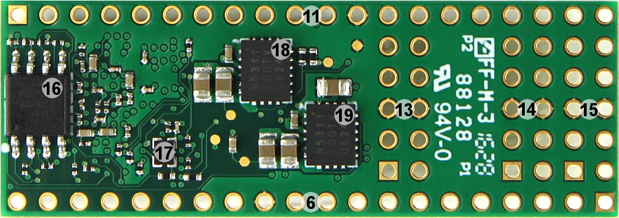
Figure 3: TE0722-02 PCB bottom side.
- Xilinx Zynq XC7Z010 or Zynq XC7Z007S SoC, U1
- Micro SD card socket with card detect, J8
- Red LED, D3
- Green LED, D2
- Red LED, D6
- 20-pin connector placeholder, P1
- Red LED, D5
- Proximity/ambient light sensor, U4
- RGB LED, D4
- Red LED, D1
- 20-pin connector placeholder, P2
- Ultra-low supply-current voltage monitor, U4
- 2 x 5-pin connector placeholder, J1
- 2 x 5-pin connector placeholder, J2
- 2 x 5-pin connector placeholder, J3
- 16 MByte QSPI Flash memory, U5
- Low-power programmable oscillator @ 33.333333 MHz, U8
- 1A PowerSoC DC-DC converter (1.0V), U2
- 1A PowerSoC DC-DC converter (1.8V), U3
Initial Delivery State
Storage device name | Content | Notes |
|---|---|---|
Quad SPI Flash | Empty |
Table 1: . Initial delivery state of programmable devices on the module
Boot Process
By default the ... supports QSPI and SD Card boot modes which is controlled by the MODE input signal from the B2B connector JM..
...
High or open
...
SD Card
...
Low or ground
...
QSPI Interface
The 7 boot mode strapping pins (MIO2 ... MIO8) of the Xiliny Zynq Z-7010 device are hardware programmed on the board. They are evaluated by the Zynq device soon after the 'POR_B'.signal is deasserted to begin the boot process (see section "Boot Mode Pin Settings" of Xilinx manual UG585).
The TE0722 FPGA board is hardware programmed to boot initially from the on-board QSPI Flash memory U5. The JTAG interface of the module is provided for storing the data to the QSPI Flash memory through the Zynq Table 2: Selecting power-on boot device.
Signals, Interfaces and Pins
I/O Signals on Connectors
Overview of the PL I/O banks signals routed to the external connectors:
| Bank | Type | Connector | I/O Signal Count | Voltage | Notes |
|---|---|---|---|---|---|
| 34 | HR | P1 | 8 | 3.3V | Signal Schematic names: 'P0' - 'P7' |
| 34 | HR | P2 | 8 | 3.3V | Signal Schematic names: 'P24' - 'P31' |
| 34 | HR | P2 | 10 , 5 LVDS single ended I/O's or 5 differential pairs | 3.3V | - |
| 34 | HR | J1 | 6 | 3.3V | Signal Schematic names: 'X2A' - 'X2F' |
| 34 | HR | J2 | 2 | 3.3V | - |
| 34 | HR | J3 | 4 | 3.3V | Signal Schematic names: 'X1A' - 'X1D' |
| 35 | HR | P1 | 8 , 4 LVDS single ended I/O's or 4 differential pairs | 3.3V | - |
Table 32: Zynq SoC PL I/O signals overview
Zynq SoC I/O Banks
| Bank | Type | VCCIO | I/O Signal Count | Available on Connectors | Notes |
|---|---|---|---|---|---|
| 34 | HR | 3.3V | 41 | 38 | 38 user I/O's, 3 I/O's used for controlling the RGB LED D4. |
| 35 | HR | 3.3V | 8 | 8 | 8 single ended or 4 differential. |
| 500 | PS MIO | 3.3V | 7 | - | 6 MIO pins used for QSPI flash memory interface, 1 MIO pin connected to green LED D2. |
| 501 | PS MIO | 3.3V | 10 | - | 7 MIO pins used for SD Card interface, 3 MIO pins connected to light sensor U4. |
| 0 | Config | 3.3V | 5 | - | 4 I/O's are dedicated to JTAG interface, 'DONE'-signal is indicated by red LED D6. |
Table 3: General overview of Zynq SoC PL/PS I/O banks
JTAG Interface
JTAG access to the Xilinx ZYNQ XC7Z010 SoC is provided through J2 connector.:
JTAG Signal | J2 Connector Pin |
|---|---|
| TCK | 4 |
| TDI | 9 |
| TDO | 10 |
| TMS | 8 |
Table 4: JTAG interface signals.
Quad SPI Interface
Quad SPI Flash memory (U5) is connected to the Zynq SoC PS QSPI0 interface via PS MIO bank 500, pins MIO1 ... MIO6.:
| Zynq SoC's MIO-pin | U5 Pin | Signal Schematic Name | U5 Pin|
|---|---|---|---|
| MIO1 | 1 | SPI0-CS | 1|
| MIO2 | 25 | SPI0-DQ0/M0 | |
| 5MIO3 | 32 | SPI0-DQ1/M1 | |
| 2MIO4 | 43 | SPI0-DQ2/M2 | |
| 3MIO5 | 57 | SPI0-DQ3/M3 | 7|
| MIO6 | 6 | SPI0-SCK | 6
Table 5: Quad SPI interface signals and connections.
SD Card Interface
TE0722 module board has on-board 3.3V SD Card socket (J8) with card detect switch wired to the Zynq SoC PS MIO bank 501, pins MIO28 .. MIO33 and MIO49.
| Zynq SoC's MIO-pin | Connected ToJ8 pin | Signal Schematic Name |
|---|---|---|
| 28MIO28 | J8-7 | DAT0 |
| 29MIO29 | J8-3 | CMD |
| 30MIO30 | J8-5 | CLK |
| 31MIO31 | J8-8 | DAT1 |
| 32MIO32 | J8-1 | DAT2 |
| 33MIO33 | J8-2 | CD/DAT3 |
| 49MIO49 | J8-G4 | Card detect switch |
Table 6: SD card interface signals.
...
I²C Interface
I2C interface pins SCL and SDA from the Zynq SoC PL bank 34 are connected to the connector J1. There are no on-board I2C slave devicesPS MIO-bank 501 (MIO36, MIO37) are connected to ambient / proximity light sensor (U4).
| Zynq SoC's MIO-pin | Connected ToU4 pin | Signal Schematic Name |
|---|---|---|
| MIO36 | U4-2 | SCL |
| MIO37 | U4-1 | SDA |
Table 7: Zynq SoC I2C interface signals.
Default PS MIO Mapping
| MIO-pin | Function | Connector Pin | Notes | 7 | GPIO | -to |
|---|---|---|---|---|---|---|
| MIO1 | QSPI | QSPI flash memory, pin 1 | ||||
| MIO2 | QSPI | QSPI flash memory, pin 5 | ||||
| MIO3 | QSPI | QSPI flash memory, pin 2 | ||||
| MIO4 | QSPI | QSPI flash memory, pin 7 | ||||
| MIO5 | QSPI | QSPI flash memory, pin 3 | ||||
| MIO6 | QSPI | QSPI flash memory, pin 6 | ||||
| MIO7 | GPIO | Green LED D2 | ||||
| 39 | GPIO | - | Si1143 INT pin | |||
| MIO28 | SDIO | SD Card socket. pin J8-5 | ||||
| MIO29 | SDIO | SD Card socket. pin J8-3 | ||||
| MIO30 | SDIO | SD Card socket. pin J8-7 | ||||
| MIO31 | SDIO | SD Card socket. pin J8-8 | ||||
| MIO32 | SDIO | SD Card socket. pin J8-1 | ||||
| MIO33 | SDIO | SD Card socket. pin J8-2 | ||||
| MIO36 | I²C | Ambient / Proximity Light Sensor U4, pin 2 | ||||
| MIO37 | I²C | Ambient / Proximity Light Sensor U4, pin 1 | ||||
| MIO39 | GPIO | Ambient / Proximity Light Sensor U4, Interrupt pin 4 | ||||
| MIO49 | GPIO | SD Card socket card detect pin J8-G4 |
Table 8: Default mapping of Zynq PS MIO-bank pinsTable 8: .
On-board Peripherals
Quad SPI Flash Memory
On-board QSPI flash memory (U5) is provided by Cypress Semiconductor Serial Flash Memory S25FL127SABMFV101 with 128 MBit (16 MByte) storage capacity. This non volatile memory is used to store initial configuration data. Besides initial configuration data, remaining free flash memory can be used for user application and data storage.
Proximity and Ambient Light Sensor
...
The TE0722-02 Zynq SoC board is equipped with the Si1143 infrared proximity and ambient light sensor. On-board three red LEDs D1, D3 and D5 are connected to the light sensor to use the proximity sensing functionality. For more details and how to configure and use this chip, refer to the Si1141/42/43 data sheet.
Oscillator
The Zynq SoC board one reference clocking signal as system clock provided by on-board oscillator U8:
| Clock Source | Frequency | Clock Input Destination |
|---|---|---|
| SiTime SiT8008AI Oscillator, U8 | 33.333333 MHz | Zynq PS Bank 500, pin C7 |
Table 9: Clock sources overview
On-board LEDs
There are 6 LEDs fitted on the Zynq SoC board. The LEDs are user configurable to indicate for example any system status.
| LED | Color | Connected Toto | Signal Schematic Name | Description and Notes | |
|---|---|---|---|---|---|
| D1 | Red | LED2, U4 | Light sensor U4, pin 6 | - | Proximity sensing functionality of light sensor U4 |
| D2 | Green | Zynq PS bank 500 | MIO7, U1User controlled, default OFF (when PS7 has not been booted). | user configurable | |
| D3 | Red | LED1, U4 | Light sensor U4, pin 9 | - | Proximity sensing functionality of light sensor U4 |
| D4 | RGB | Zynq PL bank 34, pins J15, L14, K12 | RGB_R, U1, RGB_G, U1, RGB_B, U1 | user configurable | |
| D5 | Red | Light sensor U4, pin 7 | - | Proximity sensing functionality of light sensor LED3, U4 | |
D6 | Green | Zynq config bank 0 | DONE, U1 | Reflects inverted DONE signal. ON when FPGA is not configured, |
Table 9: .10: LEDs of the board
Connectors
All connectors are for 100mil (2.54mm pitch) headers, all connector locations are in 100mil grid. The module's PCB provides footprints to mount and solder optional pin headers, if those are not factory-fitted on module.
Power and Power-On Sequence
Power Consumption
Power To power-up a module, power supply with minimum current capability of 1A is recommended.
Power Supply
TE0722-02 needs one single power supply with nominal of 3.3V at all variants. Following diagram shows the dependencies of the power supply:
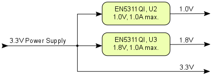
Figure 4: Module power supply dependencies
Power Consumption
| Board Variant | FPGA | Design | Typical Power, 25°C ambient |
|---|---|---|---|
| TE0722-02I | XC7Z010-1CLG225I | Not configured | TBD* |
| TE0722-02 | XC7Z010-1CLG225C | Not configured | TBD* |
| TE0722-02-07S-1C | XC7Z007S-1CLG225C | Not configured | TBD* |
Table 11: Module power consumption
*TBD - To Be Determined.
for system startup is recommended. The maximum power consumption of the module mainly depends on the design running on the Zynq SoC's FPGA and ambient temperature.
Xilinx provide a power estimator excel sheets to calculate power consumption. It is also possible to evaluate the power consumption of the developed design with Vivado. See also Trenz Electronic Wiki FAQ.
Typical power consumption is to be determined.
Power-On Sequence
... diagram will be here soon ...
Variants Currently in Production
Power-On Sequence
There is no specific or special power-on sequence, single power source is needed as 3.3V as power supply voltage.
Voltage Monitor Circuit
The voltages 1.0V (core voltage) and 3.3V are monitored by the voltage monitor circuit U6, which generates the POR_B reset signal at power-on. A manual reset is also possible by driving the connector pin P1-10 ('NRST') to GND. Leave this pin unconnected or connect to VDD (3.3V) when unused.
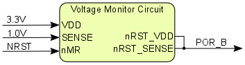
Figure 5: Voltage monitor circuit
Power Rails
Power Rail Name | J1 Pins | J2 Pins | J3 Pins | P1 Pin | P2 Pin | Direction | Notes |
|---|---|---|---|---|---|---|---|
| 3.3V | 5, 6 | 5, 6 | 5, 6 | 12 | 12 | Input | 3.3V power supply voltage |
Table 12: Board power rails
Bank Voltages
Bank | Bank I/O Voltage VCCO | Voltage Range |
|---|---|---|
| 0 (config) | 3.3V | fixed |
| 500 (MIO) | 3.3V | fixed |
| 501 (MIO) | 3.3V | fixed |
| 34 (HR) | 3.3V | fixed |
| 35 (HR) | 3.3V | fixed |
Table 13: Board bank voltages
Variants Currently in Production
| Board Module Variant | Xilinx Zynq SoC | ARM Cores | PL Cells | LUTs | Flip-Flops | Block RAM | DSP Slices | Zynq SoC Operating Temperature Temperature Temp. | Temp. Range |
|---|---|---|---|---|---|---|---|---|---|
| TE0722-02I | XC7Z010-1CLG225I | A9+ Dual-core | 28K | 17,6K | 35,2K | 2.1 MBytes | 80 | –40°C to +85°C100°C | Industrial |
| TE0722-02 | XC7Z010-1CLG225C | A9+ Dual-core | 28K | 17,6K | 35,2K | 2.1 MBytes | 80 | 0°C to +70°C85°C | Commercial |
| TE0722-02-07S-1C | XC7Z007S-1CLG225C | A9+ Single-core | 23K | 14,4K | 28,8K | 1.8 MBytes | 66 | 0°C to +70°C85°C | Commercial |
Table 814: Module Board variants.
Technical Specifications
Absolute Maximum Ratings
Parameter | Min | Max | Units | Reference Document |
|---|
3.3 supply voltage | -0. |
| 3 | 3.6 | V | EN5311QI datasheet / Xilinx datasheet DS187 |
| HR PL I/O banks input voltage (VCCIO single ended) | -0.4 | VCCO + 0.55 | V | Xilinx datasheet DS187 (VCCO 3.3V nominal) |
Storage temperature | -40 | +85 | °C | Silicon Labs Si1141/42/43 datasheet. |
Table 915: Module Board absolute maximum ratings.
Recommended Operating Conditions
| Parameter | Min | Max | Units | Reference Document |
|---|
| 3.3 supply voltage |
| 3. |
| 3 | 3.465 | V | Xilinx datasheet DS187 |
Table 10: Module recommended operating conditions.
| HR PL I/O banks input voltage (VCCIO single ended) | -0.20 | VCCO + 0.20 | V | Xilinx datasheet DS187 (VCCO 3.3V nominal) |
Operating Temperature Commercial | 0 | +85 | °C | Xilinx datasheet DS190 |
Operating Temperature Industrial | -40 | +85 | Xilinx datasheet DS190 |
Table 16: Board recommended operating condition
| Note |
|---|
| Please check Xilinx datasheet DS187 for complete list of absolute maximum and recommended operating ratings for the Zynq-7 device |
| Note |
| Assembly variants for higher storage temperature range are available on request. |
Physical Dimensions
Module size: 18 17.9 mm × 51 mm. Please download the assembly diagram for exact numbers.
PCB thickness: 1.6 65 mm.
Highest part on PCB approx. 4 mm. Please download the step model for exact numbers.
All dimensions are given in millimeters.
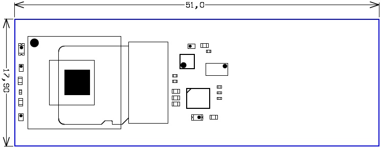
Figure 46: TE0722-02 Board physical dimensions.
Operating Temperature Ranges
Commercial grade: 0°C to +70°C.
Industrial grade: -40°C to +85°C.
Operating temperature range depends also on customer design and cooling solution. Please contact us for options.
Revision History
Hardware Revision History
| Date | Revision | Notes | PCN | Documentation Link |
|---|---|---|---|---|
| 2015-10-23 | 02 | - | - | TE0722-02 |
| - | 01 | First production release | - | - |
Table 1117: TE0722 module Board hardware revision history.
Hardware revision number is printed on the PCB board together with the module model number separated by the dash.

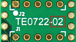
Figure 57: TE0722 module hardware revision number.
Document Change History
Date | Revision | Contributors | Description | ||||||||
|---|---|---|---|---|---|---|---|---|---|---|---|
| Ali Naseri, Jan Kumann | Initial document.
|
Table 1218: Document change history.
Disclaimer
| Include Page | ||||
|---|---|---|---|---|
|
Overview
Content Tools