Page History
...
| Power Input Pin | Max Current |
|---|---|
| VIN | 4A |
Typical The power-consumption for of TE0706-02 in conjunction with different 4x5 SoMs under certain configurations will be determined soonare depending on the used model of the 4x5 SoM and the custom-made FPGA-design on this SoM. Please refer to the TRM of the mounted 4x5 SoM to get information about the typical power consumption.
Power-On Sequence
It is not allowed to feed any voltage to any external I/O pin before there is no power indication on M3.3VOUT pins. Presence of 3.3V on B2B JB2 connector pins 9 and 11 indicates that module is properly powered up and ready. The 1.8V voltage-level on base-board for supplying PL I/O bank supply-voltages will be available after the module's 3.3V voltage-level has reached stable state on the B2B JB2 connector pins 9 and 11.
If VCCIOA or VCCIOC will be powered through the dedicated pins of external connector J6, then corresponding VCCIO jumpers J10 and J12 should be removed.
...
| Note |
|---|
Note: The corresponding PL I/O bank supply voltages of the 4x5 SoM to the selectable baseboard voltages VCCIOA, VCCIOB and VCCIOC are depending on the mounted 4x5 SoM and varying in order of the used model. Refer to the SoMs schematic for information about the specific pin assignments on module's B2B-connectors regarding the PL I/O bank supply voltages and to the 4x5 Module integration Guide for VCCIO voltage options. |
Base-board supply-voltages (Following table describes how baseboard supply voltages VCCIOA, VCCIOB, VCCIOC and 1.8V are connected to the PL I/O bank voltages on different supported 4x5 SoMs:
...
Baseboard supply voltage
...
TE0715
xx-15
...
TE0715
xx-30
...
Bank 15,
VCCIOA
...
Bank 15,
VCCIOA
...
Bank 16,
VCCIOA
...
Bank 16,
VCCIOA
...
Bank 13,
VCCIOA
...
Bank 13,
VCCIOA
...
Bank 35,
VCCIOA
...
Bank 13,
VCCIOA
...
Bank 64,
VCCIOA
...
-
...
-
...
-
...
Bank 34,
VCCIOC
...
Bank 34,
HP bank,
VCCIOC
...
Bank 33,
VCCIOC
...
Bank 15,
VCCIOC
...
Bank 68,
HP bank,
VCCIOC
...
Bank 34,
VCCIOD
...
Bank 35,
VCCIOD
...
Bank 15,
VCCIOD
...
Bank 15,
VCCIOD
...
Bank 35,
VCCIOD
...
Bank 35,
HP bank,
VCCIOD
...
Bank 13,
VCCIOD
...
Bank 12,
VCCIOD
...
Bank 67,
HP bank,
VCCIOD
...
Bank 34,
VCCIOB
...
Bank 13,
VCCIOB
...
Bank 13,
VCCIOB
...
Bank 34,
VCCIOB
...
Bank 16,
VCCIOB
...
Bank 66,
HP bank,
VCCIOB
) configuration-jumpers.
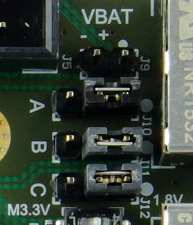
Following table shows how to configure the voltage-levels of base-board supply-voltages VCCIOA, VCCIOB and VCCIOC by jumper, 0-Ohm-resistor or by feeding the supply voltage through connector J6:
| supply-voltage by jumper | supply-voltage by 0-Ohm-resistor | supply-voltage by connector J6 | ||||
|---|---|---|---|---|---|---|
| voltage level | 1.8V | 3.3V | 1.8V | 3.3V | variable | |
| VCCIOA | J10: 1-2, 3 | J10: 1, 2-3 | - | R20 | J6 pin B32 | |
| VCCIOB | J11: 1-2, 3 | J11: 1, 2-3 | R29 | R21 | - | |
| VCCIOC | J12: 1-2, 3 | J12: 1, 2-3 | R30 | R22 | J6 pin B1 | |
Only one supply-source is allowed to configure the base-board supply-voltages, either by jumper, 0-Ohm-resistor or connector J6. If a supply-voltages is configured by 0-Ohm-resistor or connector J6, then the corresponding configuration-jumper has to be removed. There aren't 0-Ohm-resistors and supply-voltages by connector J6 allowed if the corresponding base-board supply-voltage is configured by jumper. Vice versa jumpers and 0-Ohm-resistors have to be removed if supplying corresponding base-board supply-voltage by connector J6.
Note: If supplying base-board supply-voltages by connector J6, the module's internal 3.3V voltage-level on pins 9 and 11 of B2B-connector JB2 has to reached stable state.
Jumper settings to configure VCCIOA, VCCIOB and VCCIOC voltages supplied by the baseboard.
...
Jumper J10
...
VCCIOA
...
Jumper J11
...
Jumper J12
...
| Note |
|---|
| It is recommended to set and measure the PL IO-bank supply-voltages before mounting of TE 4x5 module , to avoid failures and damages to the functionality of the mounted SoM. |
...
Overview
Content Tools