Page History
...
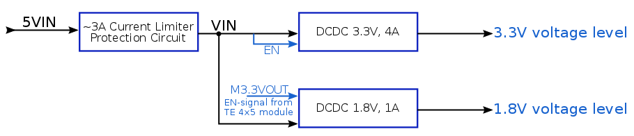
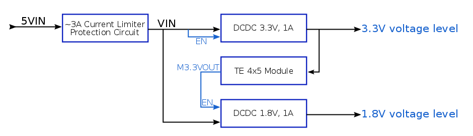
It is not allowed to feed any voltage to any external I/O pin before there is no power indication on M3.3VOUT pins. Presence of 3.3V on B2B JB2 connector pins 9 and 11 indicates that module is properly powered up and ready. The 1.8V voltage-level on base-board for supplying PL I/O bank supply-voltages will be available after the module's 3.3V voltage-level has reached stable state on the B2B JB2 connector pins 9 and 11.
If VCCIOA or VCCIOC will be powered through the dedicated pins of external connector J6, then corresponding VCCIO jumpers J10 and J12 should be removed.
...
Overview
Content Tools