Page History
...
| Scroll Title | ||||||||||||||||||||||||||||||||||
|---|---|---|---|---|---|---|---|---|---|---|---|---|---|---|---|---|---|---|---|---|---|---|---|---|---|---|---|---|---|---|---|---|---|---|
| ||||||||||||||||||||||||||||||||||
|
Main Component
| Scroll Title | ||||||||||||||||||||||||||||||||||
|---|---|---|---|---|---|---|---|---|---|---|---|---|---|---|---|---|---|---|---|---|---|---|---|---|---|---|---|---|---|---|---|---|---|---|
| ||||||||||||||||||||||||||||||||||
|
...
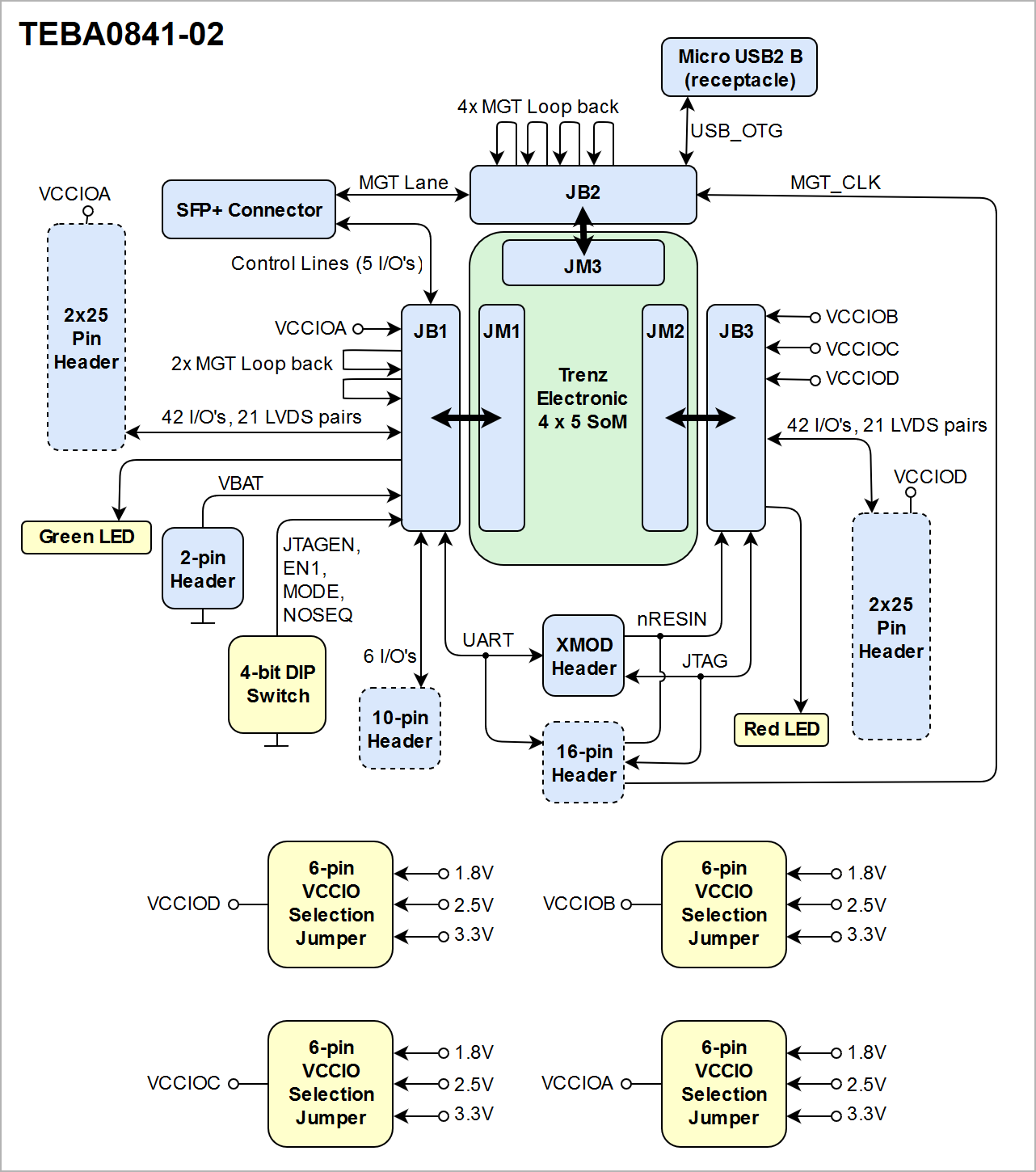
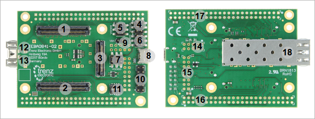
- Samtec Razor Beam™ LSHM-150 B2B connector, JB1
- Samtec Razor Beam™ LSHM-150 B2B connector, JB3
- Samtec Razor Beam™ LSHM-130 B2B connector, JB2
- 6-pin header J26, for selecting PL I/O-bank voltage
- 6-pin header J27J5, for selecting PL I/O-bank voltage
- Micro USB2 Type B connector J12 (Device or OTG mode)
- XMOD FTDI JTAG/UART header, JX1
- 6-pin header J6, for selecting PL I/O-bank voltage
- 6-pin header J27, for selecting PL I/O-bank voltage
- Micro USB2 Type B connector J10 (Device or OTG mode)
- 2-pin VBAT header J7
- XMOD FTDI JTAG/UART header, JX1
- 4-bit DIP-switch S1
- User User LED D1 (green)
- User LED D2 (red)
- SFP+ Connector, J1
- 5010-pin header soldering-pads J17, for access to PL J4, 6 I/O-bank pins (42 I/O'S, 21 LVDS pairs's available
- 16-pin header soldering-pads J3, JTAG/UART header ('XMOD FTDI JTAG Adapter'-compatible pin-assignment)
- 50-pin header soldering-pads J20J17, for access to PL I/O-bank pins (42 I/O'S, 21 LVDS pairs)
- 1650-pin header soldering-pads J3, JTAG/UART header ('XMOD FTDI JTAG Adapter'-compatible pin-assignment)10-pin header soldering-pads J4, 6 I/O's availableJ20, for access to PL I/O-bank pins (42 I/O'S, 21 LVDS pairs)
- SFP+ Connector, J1
Initial Delivery State
Board is shipped in following configuration:
...
Following table gives a summary of the available I/O's, interfaces and differential pairs of the mounted SoM on the B2B connectors JB1, JB2 and JB3 of the carrier board:
| B2B Connector | Interfaces | I/O Signal Count | LVDS-pairs count | Connected to | Notes |
|---|---|---|---|---|---|
| JB1 | I/O | 42 | 21 | 2x25-pin header J20 | - |
| 6 | - | 10-pin header J4 | - | ||
| Control signals | 5 | - | SFP+ connector J1 | 'TX FAULT', 'MOD-DEF0' ... 'MOD-DEF2', 'LOS' | |
| 4 | - | DIP switch S1 | 'JTAGEN (BOOTMODE)', 'EN1', 'MODE', 'NOSEQ' | ||
| 1 | - | Green LED D1 | user LED | ||
| UART | 2 | - | XMOD header JX1, 16-pin header J3 | also usable as GPIO's | |
| MGT | - | 4 (2 MGT lanes) | 2x loop back circuit on B2B connector JB1 | - | |
| JB2 | USB | - | 1 | Micro USB2 Type B connector J10 | - |
| MGT | - | 2 (1 MGT lanes) | SFP+ connector J1 | - | |
| - | 8 (4 MGT lanes) | 4x loop back circuit on B2B connector JB2 | - | ||
| Clock | - | 1 | MGT clock input from 16-pin header J3 | - | |
| JB3 | I/O | 42 | 21 | 2x25-pin header J17 | - |
| JTAG | 4 | - | XMOD header JX1, 16-pin header J3 | - | |
| Control signals | 1 | - | XMOD header JX1, 16-pin header J3 | 'RESIN', nRESET signal to mounted SoM | |
| 1 | - | Red LED D2 | user LED |
Table 1: General overview of PL I/O signals and SoM's interfaces connected to the B2B connectors
...
Following table gives a summary of the pin-assignment, available interfaces and functional I/O's of the pin headers:
| On-board Pin Header | Signals and Interfaces | Count of I/O's | Notes |
|---|---|---|---|
| J17 | User I/O | 42 single ended or 21 differential | - |
| J20 | User I/O | 42 single ended or 21 differential | - |
| JX1 | JTAG | 4 | - |
| Control signals | 1 | 'RESIN' | |
| I/O's | 2 | user IO (configurable as UART) | |
| J3 | JTAG | 4 | - |
| Control signals | 1 | 'RESIN' | |
| I/O's | 2 | user IO (configurable as UART) | |
| MGT reference input clock | 1 differential pair | AC decoupled on-board (100 nF capacitor) | |
| J4 | User I/O | 6 single ended | 3.3V and 1.8V voltage level available on header |
Table 2: General overview of PL I/O signals, SoM's interfaces and control signals connected to the on-board connectors
...
Following table describes the pin-assignment of the SFP+ connector:
| SFP+ pin | Pin Schematic Name | B2B | FPGA Direction | Description | Note |
|---|---|---|---|---|---|
| Transmit Data + (pin 18) | MGT_TX3_P | JB2-26 | Output | SFP+ transmit data differential pair | - |
| Transmit Data - (pin 19) | MGT_TX3_N | JB2-28 | Output | - | |
| Receive Data + (pin 13) | MGT_RX3_P | JB2-25 | Input | SFP+ receive data differential pair | - |
| Receive Data - (pin 12) | MGT_RX3_N | JB2-27 | Input | - | |
| Receive Fault (pin 2) | MIO10 | JB1-96 | Input | Fault / Normal Operation | High active logic |
| Receive disable (pin 3) | SFP0_TX_DIS | not connected | Output | SFP Enabled / Disabled | Low active logic |
| MOD-DEF2 (pin 4) | MIO13 | JB1-98 | BiDir | 2-wire Serial Interface data | 3.3V pull-up on-board |
| MOD-DEF1 (pin 5) | MIO12 | JB1-100 | Output | 2-wire Serial Interface clock | 3.3V pull-up on-board |
| MOD-DEF0 (pin 6) | MIO11 | JB1-94 | Input | Module present / not present | Low active logic |
| RS0 (pin 7) | SFP0_RS0 | not connected | Output | Full RX bandwidth | Low active logic |
| LOS (pin 8) | MIO0 | JB1-88 | Input | Loss of receiver signal | High active logic |
| RS1 (pin 9) | SFP0_RS1 | not connected | Output | Reduced RX bandwidth | Low active logic |
Table 3: SFP+ connector pin-assignment
...
The MGT lane pins are routed on-board as follows, if 4 x 5 SoM TE0841 is mounted on carrier board:
| MGT Lane | B2B TX Differential Pair | B2B RX Differential Pair | B2B Pins connected |
|---|---|---|---|
| MGT-lane 0 | JB2-8 (MGT_TX0_N) JB2-10 (MGT_TX0_P) | JB2-7 (MGT_RX0_N) JB2-9 (MGT_RX0_P) | JB2-7 to JB2-8 JB2-9 to JB2-10 |
| MGT-lane 1 | JB2-14 (MGT_TX1_N) JB2-16 (MGT_TX1_P) | JB2-13 (MGT_RX1_N) JB2-15 (MGT_RX1_P) | JB2-13 to JB2-14 JB2-15 to JB2-16 |
| MGT-lane 2 | JB2-20 (MGT_TX2_N) JB2-22 (MGT_TX2_P) | JB2-19 (MGT_RX2_N) JB2-21 (MGT_RX2_P) | JB2-19 to JB2-20 JB2-21 to JB2-22 |
| MGT-lane 7 | JB2-2 (MGT_TX7_P) JB2-4 (MGT_TX7_N) | JB2-1 (MGT_RX7_P) JB2-3 (MGT_RX7_N) | JB2-1 to JB2-2 JB2-3 to JB2-4 |
| MGT-lane 4 | JB1-3 (MGT_TX4_P) JB1-5 (MGT_TX4_N) | JB1-9 (MGT_RX4_P) JB1-11 (MGT_RX4_N) | JB1-9 to JB1-3 JB1-11 to JB1-5 |
| MGT-lane 5 | JB1-15 (MGT_TX5_P) JB1-17 (MGT_TX5_N) | JB1-21 (MGT_RX5_P) JB1-23 (MGT_RX5_N) | JB1-21 to JB1-15 JB1-23 to JB1-17 |
Table 4: Looped-backed MGT-lanes for mounted 4 x 5 SoM TE0841
...
JTAG access to the mounted SoM is provided through B2B connector JB3 and is routed to the XMOD header JX1 and also to pin header J3. With the TE0790 XMOD USB2 to JTAG adapter, the FPGA device of the mounted SoM can be programed via USB2 interface.
JTAG Signal | B2B Connector Pin | XMOD Header JX1 | Pin Header J3 | Note |
|---|---|---|---|---|
| TCK | JB3-100 | JX1-4 | J3-4 | - |
| TDI | JB3-96 | JX1-10 | J3-10 | - |
| TDO | JB3-98 | JX1-8 | J3-8 | - |
| TMS | JB3-94 | JX1-12 | J3-12 | - |
Table 5: JTAG interface signals
...
Following table describes the signals and interfaces of the XMOD header JX1:
| Pin Schematic Name | XMOD Header JX1 Pin | B2B | Note |
|---|---|---|---|
| TCK | C (pin 4) | JB3-100 | - |
| TDO | D (pin 8) | JB3-98 | - |
| TDI | F (pin 10) | JB3-96 | - |
| TMS | H (pin 12) | JB3-94 | - |
| MIO15 | A (pin 3) | JB1-86 | UART-TX (transmit line) |
| MIO14 | B (pin 7) | JB1-91 | UART-RX (receive line) |
| RESIN | G (pin 11) | JB3-17 | nRESET signal to the mounted SoM |
Table 6: XMOD header JX1 signals and connections
When using XMOD FTDI JTAG Adapter TE0790, the adapter-board's VCC and VCCIO will be sourced by the on-boards 3.3V supply voltage. Set the XMOD DIP-switch with the setting:
| XMOD DIP-switches | Position |
|---|---|
| Switch 1 | ON |
| Switch 2 | OFF |
| Switch 3 | OFF |
| Switch 4 | OFF |
Table 7: XMOD adapter board DIP-switch positions for voltage configuration
...
As alternative to the XMOD header JX1, on the carrier board pin header J3 is present, which has a XMOD header-compatible pin-assignment, but also two additional pins (15,16) as differential pair to supply the mounted SoM with an external MGT reference clock signal:
| Pin Schematic Name | Header J3 Pin | B2B | Note |
|---|---|---|---|
| TCK | 4 | JB3-100 | - |
| TDO | 8 | JB3-98 | - |
| TDI | 10 | JB3-96 | - |
| TMS | 12 | JB3-94 | - |
| MIO15 | 3 | JB1-86 | UART-TX (transmit line) |
| MIO14 | 7 | JB1-91 | UART-RX (receive line) |
| RESIN | 11 | JB3-17 | nRESET signal to the mounted SoM |
| CLK0_N | 15 | JB2-32 | AC decoupled on-board (100 nF capacitor) |
| CLK0_P | 16 | JB2-34 | AC decoupled on-board (100 nF capacitor) |
Table 8: JTAG/UART header J3 signals and connections
...
UART interface is available on B2B connector JB1 established by the mounted SoM's FPGA device. With the TE0790 XMOD USB2 adapter, the UART signals can be converted to USB2 interface signals:
| UART Signal Schematic Name | B2B | XMOD Header JX1 | Pin Header J3 | Note |
|---|---|---|---|---|
| MIO14 | JB1-91 | JX1-7 | J3-7 | UART-RX (receive line) |
| MIO15 | JB1-86 | JX1-3 | J3-3 | UART-TX (transmit line) |
Table 9: UART interface signals
...
Following table gives an overview of the USB2 interface signals:
| USB2.0 Signal Schematic Name | B2B | Connected to | Note |
|---|---|---|---|
| OTG_N | JB2-48 | J10-2 | USB2 data differential pair |
| OTG_P | JB2-50 | J10-3 | |
| OTG-ID | JB2-52 | J10-4 | Ground this pin for A-Device (host), leave floating this pin for B-Device (peripheral). |
| USB-VBUS | JB2-56 | J10-1 | USB supply voltage for Host mode. Not supplied by the Carrier Board. |
Table 10: USB2 interface signals and connections
...
The on-board LEDs are available to the user and can be used to indicate system status and activities:
| LED | Color | Signal Schematic Name | Connected to | Description and Notes |
|---|---|---|---|---|
| D1 | Green | MIO9 | JB1-92 | available to user |
| D2 | Red | RLED | JB3-90 | available to user |
Table 11: On-board LEDs
DIP-Switch
There are one 4-bit DIP-witches S1 present on the TEBA0841 board to configure options and set parameters. The following table describes the of the particular switches:
| DIP-switch S1 | usage | Default | Signal Schematic Name | Connected to |
|---|
| Note | ||||
|---|---|---|---|---|
| S1-1 | OFF module FPGA access | OFF(GND) | BOOTMODE | JB1-90 |
The functionalities of all DIP-switches is dependent on the mounted
and used SoM.
The DIP-switch sets control signals, which are usually routed to the
System Controller CPLD of the mounted SoM.
So refer to the Wiki reference page of the SC CPLD firmware of the SoM.
| only used for module with CPLD | |||||
| S1-2 | OFF enabled ON disabled | OFF(VDD) | EN1 | JB1-27 | power enable, some modules can't disable power in this case it has normally the same effect like the reset pin |
| S1-3 | OFF QSPI Boot ON SD Boot | OFF(VDD) | MODE | JB1-31 | Boot mode selection, only for Zynq and ZynqMP devices, on FPGA modules not matter (always QSPI). JTAG is on all modes available |
| S1-4 | OFF enabled ON disabled | OFF(VDD) | NOSEQ | JB1-8 | power sequencing, only on some modules supported. Otherwise it's unused or can be reused by customer |
Table 12: DIP-switch S1, see also 4x5 Module Controller IOs
VCCIO Selection Jumper
On the TEBA0841 carrier board different VCCIO configurations can be selected by the jumper header J26, J27, J5 and J6.
TE 4 x 5 Modules have a standard assignment of PL-bank I/O voltages on the B2B connectors, which will be fed with I/O voltage from base-board.
Base-board PL-bank I/O Voltages | Carrier Board B2B Pins | Standard Assignment of PL-bank I/O Voltages on TE 4x5 Modules |
|---|---|---|
| VCCIOA | JB1-10, JB1-12 | VCCIOA (JM1-9, JM1-11) |
| VCCIOB | JB3-2, JB3-4 | VCCIOB (JM1-1, JM1-3) |
| VCCIOC | JB3-6 | VCCIOC (JM1-5) |
| VCCIOD | JB3-8, JB3-10 | VCCIOD (JM2-7, JM2-9) |
Table 13: Base-board PL-bank I/O voltages VCCIOA ... VCCIOD
...
Following table describes how to configure the base-board supply-voltages by jumpers:
Base-board PL-bank I/O Voltages | VCCIOA | VCCIOB | VCCIOC | VCCIOD |
|---|---|---|---|---|
| 1.8V | J26:1-2 | J5:1-2 | J6:1-2 | J27:1-2 |
| 2.5V | J26:3-4 | J5:3-4 | J6:3-4 | J27:3-4 |
| 3.3V | J26:5-6 | J5:5-6 | J6:5-6 | J27:5-6 |
Table 14: Configuration of base-board supply-voltages via jumpers. Jumper-Notification: 'Jx: 1-2' means pins 1 and 2 are connected, 'Jx: 3-4' means pins 3 and 4 are connected, and so on
...
Xilinx provide a power estimator excel sheets to calculate power consumption. It's also possible to evaluate the power consumption of the developed design with Vivado. See also Trenz Electronic Wiki FAQ.
| Power Input | Typical Current |
|---|---|
| 3.3V | TBD* |
Table 15: Typical power consumption
...
The external power-supply can be connected to the board by the following pins:
| Connector | 3.3V pin | GND pin |
|---|
JX1-5, JX1-6,
| J3 | J3-5, J3-6 | J3-1, J3-2 |
| J4 | J4-5 | J4-1, J4-2 |
| J20 | J20-5, J20-46 | J20-1 , J20-2 , J20-49 , J20-50 |
| J17 | J17-5, J17-46 | J17-1 , J17-2 , J17-49 , J17-50 |
Table 16: Connector pins capable for external 3.3V power supply
...
| Scroll Title | ||||||||||||||||||||||||||||||||||
|---|---|---|---|---|---|---|---|---|---|---|---|---|---|---|---|---|---|---|---|---|---|---|---|---|---|---|---|---|---|---|---|---|---|---|
| ||||||||||||||||||||||||||||||||||
|
Power Rails
The voltage direction of the power rails is from board and on-board connectors' view:
| Module Connector (B2B) Designator | VCC / VCCIO | Direction | Pins | Notes |
|---|---|---|---|---|
| JB1 | 3.3V | Out | 2, 4, 6, 14, 16 | 3.3V module supply voltage |
| VCCIOA | Out | 10, 12 | PL IO-bank VCCO | |
| M1.8VOUT | In | 40 | 1.8V module output voltage | |
| JB3 | 3.3V_OUT | In | 9, 11 | 3.3V module output voltage |
| 3.3V | Out | 1, 3, 5, 7 | 3.3V module supply voltage | |
| VCCIOB | Out | 2, 4 | PL IO-bank VCCO | |
| VCCIOC | Out | 6 | PL IO-bank VCCO | |
| VCCIOD | Out | 8, 10 | PL IO-bank VCCO | |
| JB2 | USB-VBUS | Out | 56 | USB Host supply voltage |
Table 17: Power pin description of B2B module connector
| On-board Pin Header Designator | VCC / VCCIO | Direction | Pins | Notes |
|---|---|---|---|---|
| J17 | 3.3V | In / Out | 5, 48 | 3.3V external supply voltage |
| VCCIOD | In / Out | 6, 45 | PL IO-bank VCCIO, depends on Jumper settings | |
| J20 | 3.3V | In / Out | 5, 48 | 3.3V external supply voltage |
| VCCIOA | In / Out | 6, 45 | PL IO-bank VCCIO, depends on Jumper settings | |
| J4 | 3.3V | Out | 5 | - |
| M1.8VOUT | Out | 6 | - |
Table 18: Power Pin description of on-board connector
| Jumper / Header Designator | VCC / VCCIO | Direction | Pins | Notes |
|---|---|---|---|---|
| J26 | VCCIOA | In | 2, 4, 6 | - |
| M1.8VOUT | Out | 1 | - | |
| 2.5V | Out | 3 | - | |
| 3.3V_OUT | Out | 5 | - | |
| J27 | VCCIOD | In | 2, 4, 6 | - |
| M1.8VOUT | Out | 1 | - | |
| 2.5V | Out | 3 | - | |
| 3.3V_OUT | Out | 5 | - | |
| J5 | VCCIOB | In | 2, 4, 6 | - |
| M1.8VOUT | Out | 1 | - | |
| 2.5V | Out | 3 | - | |
| 3.3V_OUT | Out | 5 | - | |
| J6 | VCCIOC | In | 2, 4, 6 | - |
| M1.8VOUT | Out | 1 | - | |
| 2.5V | Out | 3 | - | |
| 3.3V_OUT | Out | 5 | - | |
| J7 | VBAT | In | 1 | - |
Table 19: Power Pin description of VCCIO selection jumper pin header
| Peripheral Socket Designator | VCC / VCCIO | Direction | Pins | Notes |
|---|---|---|---|---|
| J10 | USB-VBUS | In | 1 | USB Host supply voltage |
Table 20: Power pin description of peripheral connector
| JTAG Header Designator | VCC / VCCIO | Direction | Pins | Notes |
|---|---|---|---|---|
| JX1 (XMOD) | 3.3V | Out | 5 | connected to 3.3V external supply voltage |
| VCCJTAG | Out | 6 | ||
| J3 | 3.3V | Out | 5 | connected to 3.3V external supply voltage |
| 3.3V | Out | 6 |
Table 21: Power pin description of XMOD/JTAG connector
...
Technical Specifications
Absolute Maximum Ratings
| Parameter | Min | Max | Units | Notes |
|---|---|---|---|---|
Vin supply voltage | 3.135 | 3.465 | V | 3.3V supply-voltage ± 5%, limitations of the supply voltage depend also |
Storage Temperature | -55 | 105 | °C | Molex 74441-0001 Product Specification |
Table 22: Board absolute maximum ratings
Recommended Operating Conditions
| Parameter | Min | Max | Units | Notes |
|---|---|---|---|---|
| Vin supply voltage | 3.135 | 3.465 | V | 3.3V supply-voltage ± 5%, limitations of the supply voltage depend also |
| Operating temperature | -40 | +85 | °C | Molex 74441-0001 Product Specification |
Table 23: Module recommended operating conditions
...
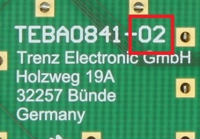
Hardware Revision History
| Date | Revision | Notes | PCN | Documentation Link |
|---|---|---|---|---|
| - | 02 |
| - | TEBA0841-02 |
| - | 01 |
| - | TEBA0841-01 |
Table 24: Module hardware revision history
...
| Scroll Title | ||||
|---|---|---|---|---|
| ||||
|
Document Change History
...
Date | Revision | Contributors | Description | ||||||||||||||||||||||||||
|---|---|---|---|---|---|---|---|---|---|---|---|---|---|---|---|---|---|---|---|---|---|---|---|---|---|---|---|---|---|
|
|
|
| ||||||||||||||||||||||||||
| 2019-09-17 | v.82 | John Hartfiel |
| ||||||||||||||||||||||||||
| 2018-07-13 | v.81 | John Hartfiel |
| ||||||||||||||||||||||||||
| 2018-07-10 | v.78 | John Hartfiel |
| ||||||||||||||||||||||||||
| v.75 | Ali Naseri, Jan Kumann |
|
...
Overview
Content Tools