Page History
...
| HTML |
|---|
<!-- Download Link: Go to Base Folder of the Module or Carrier, for example : https://shop.trenz-electronic.de/en/Download/?path=Trenz_Electronic/TE0712 Use english URL "../en/.. --> |
| Scroll Ignore |
|---|
| Scroll pdf ignore | |
|---|---|
Table of Contents
|
...
| Scroll Only (inline) |
|---|
Refer to https://wiki.trenz-electronic.de/display/PD/TEBB0714+TRM for the current online version of this manual and other available documentation.
|
The Trenz Electronic TEBB0714 is a Carrier Board for testing, evaluation and development purposes, especially for the Multi Gigabit Transceiver units of the TE0714 module. Although this base-board is dedicated to the TE0714 module, it is also compatible with other Trenz Electronic 4 x 3 cm SoMs. See page "4 x 3 cm carriers" to get information about the SoMs supported by the TEBB0714 Carrier Board.
This base-board provides also solder pads as place-holders through hole pads for pin headers as option to get access to the PL I/O-bank pins and further interfaces of the mounted TE 4 x 3 SoM.
...
Figure 1: TEBB0714-01 Block Diagram.
Main Components
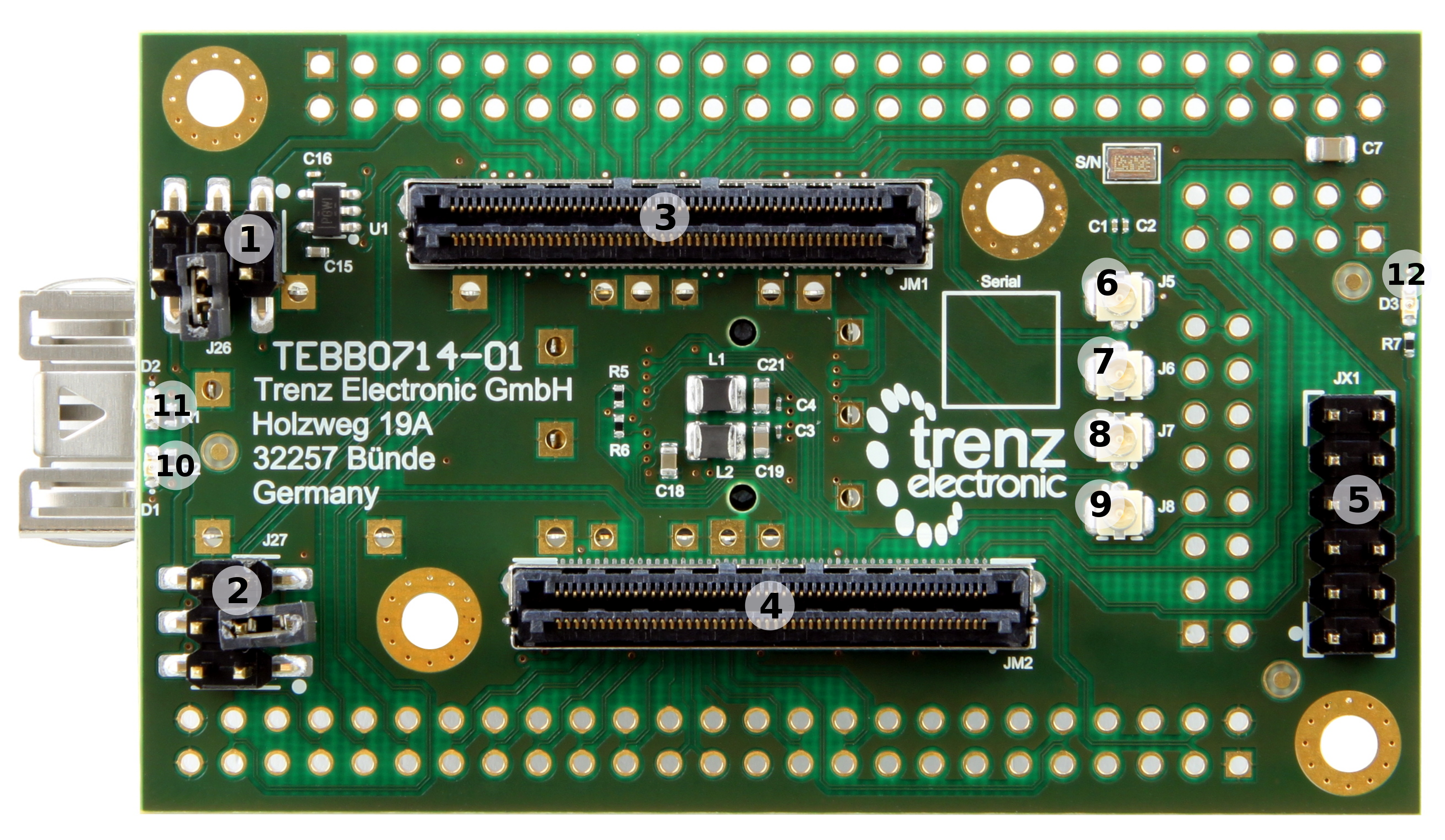
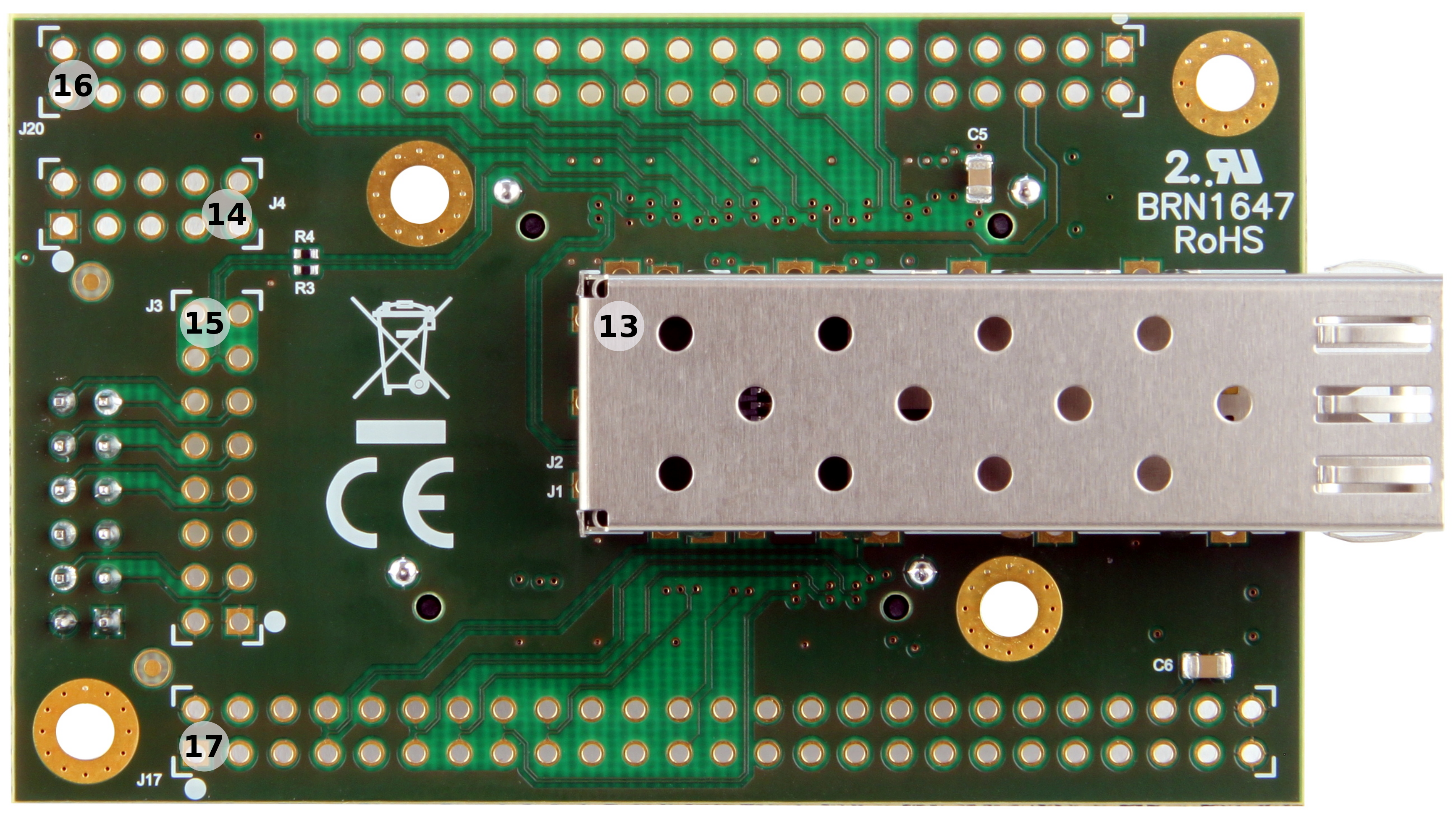
Figure 2: TEBB0714-01 Carrier Board.
- 6-pin header J26 for selecting PL-bank I/O voltage
- 6-pin header J27 for selecting XMOD/JTAG VCCIO
- Samtec Razor Beam™ LSHM-150 B2B connector, JM1
- Samtec Razor Beam™ LSHM-150 B2B connector, JM2
- XMOD header, JX1
- Ultra small SMT coaxial connector, J5
- Ultra small SMT coaxial connector, J6
- Ultra small SMT coaxial connector, J7
- Ultra small SMT coaxial connector, J8
- User LED D1 (green)
- User LED D2 (red)
- LED D3 (red) indicating FPGA's 'Programming DONE'-signal
- SFP+ Connector, J1
- 10-pin header solder pads J4 for access to SoM's PL I/O-banks (LVDS pairs possible)
- 16-pin header solder pads J3, JTAG/UART header ('XMOD FTDI JTAG Adapter'-compatible pin-assignment)with ADC and MGT clock input
- 50-pin header solder pads J20 for access to SoM's PL I/O-banks (LVDS pairs possible)
- 50-pin header solder pads J17 for access to SoM's PL I/O-banks (LVDS pairs possible)
...
| On-board Pin Header | Control Signals and Interfaces | Count of I/O's | Notes |
|---|---|---|---|
| J17 | User I/O | 36 single ended or 18 differential | - |
| QSPI interface | 6 | - | |
| J20 | User I/O | 42 single ended or 21 differential | - |
| J3 | JTAG | 4 | - |
| UART | 2 | - | |
| SoM control signals | 2 | 'BOOTMODE', 'PROG_B' | |
| ADC | 1 differential pair | - | |
| MGT reference clock input | 1 differential pair | AC decoupled on-board (100 nF capacitor) | |
| JX1 | JTAG | 4 | - |
| UART | 2 | - | |
| SoM control signals | 2 | 'BOOTMODE', 'PROG_B' | |
| J4 | User I/O | 6 single ended or 3 differential | 3.3V, 3.3V_OUT voltage level available on header |
...
| Pin Schematic Name | XMOD Header JX1 Pin | B2B | Note |
|---|---|---|---|
| TCK | C (pin 4) | JM1-90 | - |
| TDO | D (pin 8) | JM1-88 | - |
| TDI | F (pin 10) | JM1-86 | - |
| TMS | H (pin 12) | JM1-92 | - |
| B14_L25 | A (pin 3) | JM2-97 | UART -TX (transmit line(output from module to XMOD Programmer) |
| B14_L0 | B (pin 7) | JM2-99 | UART -RX (receive line(input to module from XMOD Programmer) |
| BOOTMODE | E (pin 9) | JM2-100 | - |
| PROG_B | G (pin 11) | JM1-94 | - |
...
V_CFG Value | Jumper J27 Setting | Note |
|---|---|---|
| 1.8V | pins 1-2 connected | Module's output voltage. |
| V_CFG0* | pins 3-4 connected | Internal module VCCIO: 3.3V or 1.8V (Settable by 0-Ohm-Resistor on TE0714 module). |
| 3.3V_OUT | pins 5-6 connected | Module's output voltage. |
*Default setting, do not changed, if V_CFG0 Bank power is sourced by module itself.
Table 8: Setting of reference I/O-voltage XMOD header.
| Note |
|---|
Use Xilinx compatible TE0790 adapter board (designation TE-0790-xx with out 'L') to program the Xilinx Zynq devices. The TE0790 adapter board's CPLD have to be configured with the Standard variant of the firmware. Refer to the TE0790 Resources Site for further information and firmware download. |
...
As alternative to the XMOD header JX1, on the Carrier Board pin header J3 is present , which has a XMOD header-compatible pin-assignment, but also with 4 additional pins as differential pairs to supply the mounted SoM with an external MGT reference clock signal and as to provide differential analog signal input:
| Pin Schematic Name | Header J3 Pin | B2B | Note |
|---|---|---|---|
| TCK | 4 | JM1-90 | - |
| TDO | 8 | JM1-88 | - |
| TDI | 10 | JM1-86 | - |
| TMS | 12 | JM1-92 | - |
| B14_L25 | 3 | JM2-97 | UART -TX (transmit line(output from module) |
| B14_L0 | 7 | JM2-99 | UART -RX (receive line(input to module) |
| BOOTMODE | 9 | JM2-100 | - |
| PROG_B | 11 | JM1-94 | - |
| XADC_P | 13 | JM1-25 | Analog input differential pair |
| XADC_N | 14 | JM1-27 | |
| CLK0_N | 15 | JM1-4 | AC decoupled on-board (100 nF capacitor) |
| CLK0_P | 16 | JM1-2 |
...
| UART Signal Schematic Name | B2B | XMOD Header JX1 | Pin Header J3 | Note |
|---|---|---|---|---|
| B14_L0 | JM2-99 | JX1-7 | J3-7 | UART -RX (receive line(input to module) |
| B14_L25 | JM2-97 | JX1-3 | J3-3 | UART -TX (transmit line(output from module) |
Table 10: UART interface signals.
...
Following diagram shows the distribution of the external input voltage of nominal 3.3V to the components:
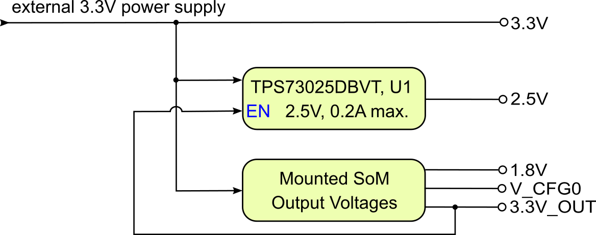
Figure 3: Board power distribution diagram.
...
The voltage direction of the power rails is from board and on-board connectors' view:
| Module Connector (B2B) Designator | VCC / VCCIO | Direction | Pins | Notes |
|---|---|---|---|---|
| JM1 | 3.3V | Out | 97, 99 | 3.3V module supply voltage |
| 3.3V_OUT | In | 83 | 3.3V module output voltage | |
| VCCIO34 | Out | 61 | PL IO-bank VCCIO | |
| JM2 | 1.8V | In | 18 | 1.8V module output voltage |
| 3.3V_OUT | Out | 54 | 3.3V module output voltage | |
| V_CFG0 | In/out | 53 | Direction depends on solder option of the modul: Internal module VCCIO |
| 3.3V or 1.8V or source from carrier is possible |
Table 16: Power pin description of B2B module connector.
...
| On-board Pin Header Designator | VCC / VCCIO | Direction | Pins | Notes |
|---|---|---|---|---|
| J17 | 3.3V | In / Out | 5, 46 | 3.3V external supply voltage |
| V_CFG | Out / int | 6, 45 | VCCIO, direction depends on jumper 27 settings and module solder option | |
| J20 | 3.3V | In / Out | 5, 46 | 3.3V external supply voltage |
| VCCIO34 | In / Out | 6, 45 | PL IO-bank VCCIO, depends on Jumper settings |
...
| Jumper / Header Designator | VCC / VCCIO | Direction | Pins | Notes |
|---|---|---|---|---|
| J26 | VCCIO34 | In | 1, 3, 5 | - |
| 1.8V | Out | 2 | - | |
| 2.5V | Out | 4 | - | |
| 3.3V_OUT | Out | 6 | - | |
| J27 | V_CFG | In / Out | 1, 3, 5- | direction depends on jumper 27 settings and module solder option |
| 1.8V | Out | 2 | - | |
| V_CFG0 | Out | 4 | - | |
| 3.3V_OUT | Out | 6 | - |
...
| JTAG/UART Header Designator | VCC / VCCIO | Direction | Pins | Notes |
|---|---|---|---|---|
| JX1 (XMOD) | 3.3V | Out | 5 | Connected to 3.3V external supply voltage |
| VIO | Out | 6 | Connected to 'V_CFG', depends on jumper 27 settings | |
| J3 | 3.3V | Out | 5 | Connected to 3.3V external supply voltage |
| V_CFG | Out | 6 | VCCIO, direction depends on jumper 27 settings and module solder option |
Table 19: Power pin description of XMOD/JTAG Connector.
Board to Board
...
Connector
| Include Page | ||||
|---|---|---|---|---|
|
Technical Specifications
...
| Parameter | Min | Max | Units | Notes |
|---|---|---|---|---|
Vin supply voltage | 3.135 | 3.465 | V | 3.3V supply-voltage ± 5% |
Storage Temperature | -40 | 85 | °C | WL-SMCW SMD chip LED data sheet |
Table 20: Board absolute Absolute maximum ratings.
Recommended Operating Conditions
| Parameter | Min | Max | Units | Notes |
|---|---|---|---|---|
| Vin supply voltage | 3.135 | 3.465 | V | - |
| Operating temperature | -40 | +85 | °C | Molex 74441-0001 Product Specification |
Table 21: Module recommended Recommended operating conditions.
Operating Temperature Ranges
Industrial grade: -40°C to +85°C.
The TEBA0841 Carrier Board itself is capable to be operated at is operable within industrial grade temperature range.
...
Physical Dimensions
Board size: PCB 46mm × 75mm. Notice that some parts the are hanging slightly over the edge of the PCB like the the SFP+ connector, which determine the total physical dimensions of the carrier board. Please download the assembly diagram for exact numbers.
Mating height of the module with standard connectors: 8mm
PCB thickness: ca. 1.65mm
Highest part on the PCB is the SFP+ connector, which has an approximately 11.3 mm overall hight. Please download the step model for exact numbers.
...
| Date | Revision | Notes | PCN | Documentation Link |
|---|---|---|---|---|
| - | 01 |
| - | TEBB0714-01 |
Table 22: Module hardware revision history.
...
Overview
Content Tools