Page History
...
| LED | Color | Connected To | Description and Notes |
|---|---|---|---|
| D2 | Red | MIO9, U1 | |
| D6 | Green | Bank 34, U1 | FPGA_LED |
| D7 | Green | 3.3V | PWR_LED |
Default PS MIO Mapping
| MIO | Function | Connected To | Notes |
|---|---|---|---|
| 0 | SDCARD | J10-9 | Card detect switch. |
| 1 | QSPI | U5-1 | SP0-CS |
| 2 | QSPI | U5-5 | SPI0-DQ0 |
| 3 | QSPI | U5-2 | SPI0-DQ1 |
| 4 | QSPI | U5-3 | SPI0-DQ2 |
| 5 | QSPI | U5-7 | SPI0-DQ3 |
| 6 | QSPI | U5-6 | SPI0-SCK |
| 7 | GPIO | U18-27 | USB PHY reset |
| 9 | LED | D2 | Red LED |
| 10 | SDCARD | J10-7 | DAT0 |
| 11 | SDCARD | J10-3 | CMD |
| 12 | SDCARD | J10-5 | CLK |
| 13 | SDCARD | J10-8 | DAT1 |
| 14 | SDCARD | J10-1 | DAT2 |
| 15 | SDCARD | J10-2 | CD/DAT3 |
| 28 | USB-OTG | U18-7 | OTG-DATA4 |
| 29 | USB-OTG | U18-31 | OTG-DIR |
| 30 | USB-OTG | U18-29 | OTG-STP |
| 31 | USB-OTG | U18-2 | OTG-NXT |
| 32 | USB-OTG | U18-3 | OTG-DATA0 |
| 33 | USB-OTG | U18-4 | OTG-DATA1 |
| 34 | USB-OTG | U18-5 | OTG-DATA2 |
| 35 | USB-OTG | U18-6 | OTG-DATA3 |
| 36 | USB-OTG | U18-1 | OTG-CLK |
| 37 | USB-OTG | U18-9 | OTG-DATA5 |
| 38 | USB-OTG | U18-10 | OTG-DATA6 |
| 39 | USB-OTG | U18-13 | OTG-DATA7 |
| 48 | ESP | J5-2 | ESP_TXD |
| 49 | ESP | J5-7 | ESP_RXD |
| 52 | ESP | J5-6 | MOD_RST |
| 53 | ESP | J5-3 | ESP_GPIO0 |
I2C Interface
I2C interface pins from the ZYNQ SoC PL bank 34 are connected to the connector J1. There are no on-board I2C slave devices.
| Signal | ZYNQ SoC Pin | Connected To |
|---|---|---|
| SDA | R13 | J1-9 |
| SCL | P13 | J1-10 |
Technical Specifications
Absolute Maximum Ratings
Parameter | Min | Max | Units | Reference Document |
|---|---|---|---|---|
VIN supply voltage | -0.5 | 3.6 | V | Xilinx datasheet DS187, "Zynq-7000 All Programmable SoC: DC and AC Switching Characteristics". |
Storage temperature | -40 | +85 | °C |
Recommended Operating Conditions
| Parameter | Min | Max | Units | Reference Document |
|---|---|---|---|---|
| Supply voltage | 1.14 | 3.465 | V | Xilinx datasheet DS187, "Zynq-7000 All Programmable SoC: DC and AC Switching Characteristics". |
| Note |
|---|
| Assembly variants for higher storage temperature range are available on request. |
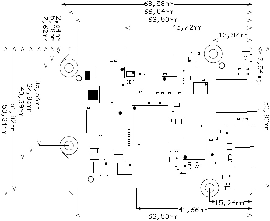
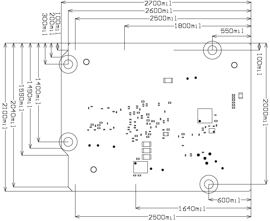
Physical Dimensions
Module size: 68.58 mm × 53.34 mm. Please download the assembly diagram for exact numbers.
PCB thickness: 1.6 mm.
Highest part on PCB: approx. 4 mm. Please download the step model for exact numbers.
Please note that two different units are used on the figures below, SI system millimeters (mm) and imperial system thousandths of an inch(mil). To convert mils to millimeters and vice versa use formula 100mil's = 2,54mm.
Operating Temperature Ranges
Commercial grade: 0°C to +70°C.
Industrial grade: -40°C to +85°C.
Operating temperature range depends also on customer design and cooling solution. Please contact us for options.
Weight
... g - Plain module
... g - Set of bolts and nuts
Revision History
Hardware Revision History
| Date | Revision | Notes | PCN | Documentation Link |
|---|---|---|---|---|
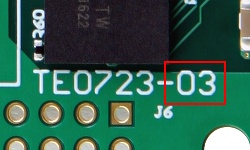
| 2016-07-15 | 03 | Click to see PCN. | TE0723-03 | |
2015-11-06 | 02 | TE0723-02 | ||
01 |
|
Hardware revision number is printed on the PCB board together with the module model number separated by the dash.
Document Change History
Date | Revision | Contributors | Description |
|---|---|---|---|
| 2017-02-11 | Jan Kumann | Initial document. |
Disclaimer
| Include Page | ||||
|---|---|---|---|---|
|
Overview
Content Tools