Page History
...
- Xilinx ZYNQ XC7Z010 SoC, U1
- 4 Gbit DDR3L 256M x 16 SDRAM, U2
- 16 MByte QSPI Flash memory, U5
High-speed CMOS logic analog multiplexer/demultiplexer, U10
- 1 MHz low-power operational amplifier, U11
- Dual high-speed USB to multipurpose UART/FIFO, U3
- 0.5A dual channel current-limited power switch, U21
- Low-power programmable oscillator @ 12.000000 MHz, U7
- 2 Kbit Microwire compatible serial EEPROM, U6
- J1
- J2
- J3
- Analog input header, J4
- J5
- PMod 2x6 interface, J6
- J7
- Micro USB 2.0 Type-B receptacle, J8
- Micro USB 2.0 Type-B receptacle, J9
- Micro SD card connector with detect signal, J10
- J11
- 5V supply power, J12
- Reset switch, S1
- Red LED, D2
- Green LED, D6
- Green LED, D7
- Ultra-low supply-current voltage monitor, U23
1A PowerSoC DC-DC converter (3.3 V), U20
- 1A PowerSoC DC-DC converter (1.8 V, U19
- 1A PowerSoC DC-DC converter (1.35 V), U16
- Hi-speed USB 2.0 ULPI transceiver, U18
- Low-power programmable oscillator @ 52.000000 MHz, U14
- 1A PowerSoC DC-DC converter (1.0 V), U17
- JTAG interface testpoints, TP1-TP4
Key Features
- Xilinx ZYNQ XC7Z010 SoC
- 16 MByte QSPI Flash
- Dual ARM Cortex A9 processors
- 512 MByte DDR3L SDRAM
- Micro SD Card socket with card detect signal
- ...
Additional assembly options are available for cost or performance optimization upon request.
...
I/O Signals
List of signals between PS/PL banks and external connectors:
| Bank | Type | Connector | I/O Signal Count | Voltage | Notes |
|---|---|---|---|---|---|
| 34 | HR | J1 | 6 | 3.3 | D8 .. 13, SDA, SCL |
| 34 | HR | J2 | 8 | 3.3 | D2 .. 7, RXD, TXD |
| 34 | HR | J6 | 8 | 3.3 | PIO01 .. PIO08 |
| 35 | HR | J4 | 7 | 3.3 | AIN0 .. 5 |
| 35 | MIO | J5 | 1 | 3.3 | ESP_GPIO2 |
| 501 | MIO | J5 | 4 | 3.3 | ESP_RXD, ESP_TXD, ESP_GPIO0, MOD_RST |
JTAG Interface
JTAG access to the Xilinx ZYNQ XC7Z010 SoC is provided through testpoints TP1-T4.
...
I2C interface pins from the ZYNQ SoC PL bank 34 are connected to the connector J1. There are no on-board I2C slave devices.
| Signal | ZYNQ SoC Pin | Connected To |
|---|---|---|
| SDA | R13 | J1-9 |
| SCL | P13 | J1-10 |
Technical Specifications
Absolute Maximum Ratings
Parameter | Min | Max | Units | Reference Document |
|---|---|---|---|---|
VIN supply voltage | -0.5 | 3.6 | V | Xilinx datasheet DS187, "Zynq-7000 All Programmable SoC: DC and AC Switching Characteristics". |
Storage temperature | -40 | +85 | °C |
Recommended Operating Conditions
| Parameter | Min | Max | Units | Reference Document |
|---|---|---|---|---|
| Supply voltage | 1.14 | 3.465 | V | Xilinx datasheet DS187, "Zynq-7000 All Programmable SoC: DC and AC Switching Characteristics". |
| Note |
|---|
| Assembly variants for higher storage temperature range are available on request. |
...
Hardware Revision History
| Date | Revision | Notes | PCN | Documentation Link |
|---|---|---|---|---|
| 2016-07-15 | 03 | Click to see PCN. | TE0723-03 | |
2015-11-06 | 02 | TE0723-02 | ||
01 |
|
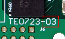
Hardware revision number is printed on the PCB board together with the module model number separated by the dash.
Document Change History
Date | Revision | Contributors | Description |
|---|---|---|---|
| 2017-02-11 | Jan Kumann | Initial document. |
Disclaimer
| Include Page | ||||
|---|---|---|---|---|
|
Overview
Content Tools