Page History
...
Interfaces and Pins
SFP+ Connector
On the The TEBB0714 Carrier Board is there provides a SFP+ connector J1 (Molex 74441-0001 ( at board-rev. 01 ). The connector is embedded into a SFP cage J2 (Molex 74737-0009 ( at board-rev. 01 ).
The RX- / TX-data-lanes are connected to B2B-connector JB2JM1, the control-lines are connected to pins on B2B-connector JB1 and are MIO-pins in standard TE module's pin-assignment.
...
The pin-assignment of the SFP connector is in detail as fellows:
| SFP+ pin | SFP+ pin netname | B2B | Note |
|---|---|---|---|
| Transmit Data + (pin 18) | MGT_TX3_P | JB2-26 | - |
| Transmit Data - (pin 19) | MGT_TX3_N | JB2-28 | - |
| Receive Data + (pin 13) | MGT_RX3_P | JB2-25 | - |
| Receive Data - (pin 12) | MGT_RX3_N | JB2-27 | - |
| Receive Fault (pin 2) | MIO10 | JB1-96 | - |
| Receive disable (pin 3) | not connected | - | - |
| MOD-DEF2 (pin 4) | MIO13 | JB1-98 | 3.3V pull-up, (usuable as SDA, I²C-Master) |
| MOD-DEF1 (pin 5) | MIO12 | JB1-100 | 3.3V pull-up, (usuable as SCL, I²C-Master) |
| MOD-DEF0 (pin 6) | MIO11 | JB1-94 | - |
| RS0 (pin 7) | not connected | - | - |
| LOS (pin 8) | MIO0 | JB1-88 | - |
| RS1 (pin 9) | not connected | - | - |
Table 1: SFP+ connector pin-assignment
...
The MGT-lane pins are bridged on-board as fellows, if 4 x 5 SoM TE0741 is mounted:
| MGT-lane | B2B TX diff-pair | B2B RX diff-pair | B2B-pins bridged |
|---|---|---|---|
| MGT-lane 0 | JB2-8 (MGT_TX0_N) JB2-10 (MGT_TX0_P) | JB2-7 (MGT_RX0_N) JB2-9 (MGT_RX0_P) | JB2-7 to JB2-8 JB2-9 to JB2-10 |
| MGT-lane 1 | JB2-14 (MGT_TX1_N) JB2-16 (MGT_TX1_P) | JB2-13 (MGT_RX1_N) JB2-15 (MGT_RX1_P) | JB2-13 to JB2-14 JB2-15 to JB2-16 |
| MGT-lane 2 | JB2-20 (MGT_TX2_N) JB2-22 (MGT_TX2_P) | JB2-19 (MGT_RX2_N) JB2-21 (MGT_RX2_P) | JB2-19 to JB2-20 JB2-21 to JB2-22 |
| MGT-lane 7 | JB1-3 (MGT_TX7_P) JB1-5 (MGT_TX7_N) | JB1-9 (MGT_RX7_P) JB1-11 (MGT_RX7_N) | JB1-3 to JB1-9 JB1-5 to JB1-11 |
| MGT-lane 6 | JB1-15 (MGT_TX6_P) JB1-17 (MGT_TX6_N) | JB1-21 (MGT_RX6_P) JB1-23 (MGT_RX6_N) | JB1-15 to JB1-21 JB1-17 to JB1-23 |
Table 2: Bridging-table of the MGT-lanes for mounted 4 x 5 SoM TE0741.
...
The JTAG-interface of the mounted 4 x 5 SoM can be accessed via header JX1. This header has a 'XMOD FTDI JTAG Adapter'-compatible pin-assignment.
| JX1 pin | JX1 pin net-name | B2B |
|---|---|---|
| C (pin 4) | TCK | JB3-100 |
| D (pin 8) | TDO | JB3-98 |
| F (pin 10) | TDI | JB3-96 |
| H (pin 12) | TMS | JB3-94 |
| A (pin 3) | MIO15 | JB1-86 |
| B (pin 7) | MIO14 | JB1-91 |
| E (pin 9) | BOOTMODE | JB1-90 (JTAGSELECT) |
| G (pin 11) | RESIN | JB3-17 |
Table 3: JTAG header JX1 pin-assignment
...
The external power-supply can be connected to the board by the following pins:
| Connector | 3.3V pin | GND pin |
|---|---|---|
| JX1 | JX1-5, JX1-6, | JX1-1, JX1-2 |
| J3 | J3-5, J3-6 | J3-1, J3-2 |
| J4 | J4-5 | J4-1, J4-2 |
| J20 | J20-5, J20-46 | J20-1 , J20-2 , J20-49 , J20-50 |
| J17 | J17-5, J17-46 | J17-1 , J17-2 , J17-49 , J17-50 |
Table 4: Connector-pins capable for external 3.3V power-supply
...
On the TEBA0841 carrier board the PL IO-bank's supply voltages of the 4x5 SoM (VCCIOA, VCCIOD; see 4x5 Module Integration Guide) are connected to the base-board VCCIO-voltage VCCIOA and VCCIOD, which are selectable between the supply-voltages 1.8V, 2.5V and 3.3V via jumper J26 and J27.
baseboard supply-voltages | base-board B2B connector-pins | standard assignment of PL IO-bank supply-voltages on TE 4x5 module's B2B connectors-pins |
|---|---|---|
| VCCIOA | JB1-10, JB1-12 | VCCIOA (JM1-9, JM1-11) |
| VCCIOD | JB2-8, JB2-10 | VCCIOD (JM2-7, JM2-9) |
Table 5: base-board supply-voltages VCCIOA and VCCIOD
| Note |
|---|
Note: The corresponding PL IO-voltage supply voltages of the 4x5 SoM to the selectable base-board voltage VCCIOA and VCCIOD are depending on the mounted 4x5 SoM and varying in order of the used model. Refer to SoM's schematic to get information about the specific pin-assignment on module's B2B-connectors regarding PL IO-bank supply-voltages and to the 4x5 Module integration Guide for VCCIO voltage options. |
Following table describes how to configure the base-board supply-voltages by jumpers:
base-board supply-voltages vs voltage-levels | VCCIOA | VCCIOD |
|---|---|---|
| 1.8V | J26:1-2 | J27:1-2 |
| 2.5V | J26:3-4 | J27:3-4 |
| 3.3V | J26:5-6 | J27:5-6 |
Table 6: Configuration of base-board supply-voltages via jumpers. Jumper-Notification: 'Jx: 1-2' means pins 1 and 2 are connected, 'Jx: 3-4' means pins 3 and 4 are connected, and so on.
| Note |
|---|
| It is recommended to set and measure the PL IO-bank supply-voltages before mounting of TE 4x5 module to avoid failures and damages to the functionality of the mounted SoM. |
Technical Specifications
Absolute Maximum Ratings
| Parameter | Min | Max | Units | Notes |
|---|---|---|---|---|
Vin supply voltage | 3.135 | 3.465 | V | 3.3V supply-voltage ± 5% |
Storage Temperature | -55 | 105 | °C | Molex 74441-0001 Product Specification |
Recommended Operating Conditions
| Parameter | Min | Max | Units | Notes |
|---|---|---|---|---|
| Vin supply voltage | 3.135 | 3.465 | V | - |
Physical Dimensions
Board size: PCB 56.47 mm × 75 mm. Notice that some parts the are hanging slightly over the edge of the PCB like the mini USB-jacks and the SFP+ connector, which determine the total physical dimensions of the carrier board. Please download the assembly diagram for exact numbers.
Mating height of the module with standard connectors: 8mm
PCB thickness: ca. 1.65mm
Highest part on the PCB is the SFP+ connector, which has an approximately 11.3 mm overall hight. Please download the step model for exact numbers.
...
ca. 32 g - Plain board
Document Change History
| date | revision | authors | description |
|---|---|---|---|
| 2017-02-08 | Ali Naseri | current TRM for TEBA0841-01 | |
| 2017-01-30 | 0.1 | Ali Naseri | Initial document |
Hardware Revision History
| Date | Revision | Notes | PCN | Documentation link |
|---|---|---|---|---|
| - | 01 |
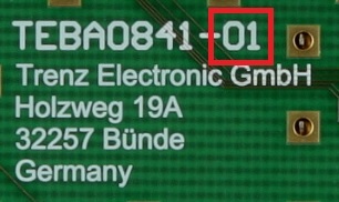
Figure 5: Hardware revision Number
...
Overview
Content Tools