Page History
...
- SFP+ connector (Enhanced small form-factor pluggable), supports data transmission rates up to 10 Gbit/s
- 4 Hirose Ultra small SMT coaxial connectors, supports data transmission rates up to 6 Gbit/s
- TE 4 x 5 cm SoM programable by JTAG header (JX1)
- 2 x user LEDs routed to IO-pins of the SoM
- Soldering-pads J17 and J20 as place-holder for further possibilities to access to SoMs SoM's IO-bank-pins, usable as LVDS-pairs
- Soldering-pads J3 and J4 as place-holder for access to JTAG- or IO-ports further interfaces and IO's of the SoM
Interfaces and Pins
...
The pin-assignment of the SFP connector is in detail as fellows:
| SFP+ pin | SFP+ pin netnamenet-name | B2B | Note |
|---|---|---|---|
| Transmit Data + (pin 18) | MGT_TX2_P | JM1-14 | - |
| Transmit Data - (pin 19) | MGT_TX2_N | JM1-16 | - |
| Receive Data + (pin 13) | MGT_RX2_P | JM1-7 | - |
| Receive Data - (pin 12) | MGT_RX2_N | JM1-9 | - |
| Transmit Fault (pin 2) | SFP0_TX_FAULT | JM2-42 | - |
| Transmit disable (pin 3) | SFP0_TX_DIS | JM2-44 | - |
| MOD-DEF2 (pin 4) | SFP0_SDA | JM2-46 | 3.3V pull-up, (usable as I²C-SDA) |
| MOD-DEF1 (pin 5) | SFP0_SCL | JM2-48 | 3.3V pull-up, (usable as I²C-SCL) |
| MOD-DEF0 (pin 6) | SFP0_M0DEF0 | JM2-40 | - |
| RS0 (pin 7) | SFP0_RS0 | JM2-38 | - |
| LOS (pin 8) | SFP0_LOS | JM2-34 | - |
| RS1 (pin 9) | SFP0_RS1 | JM2-32 | - |
Table 1: SFP+ connector pin-assignment
Ultra small SMT coaxial
...
connectors
4 HIROSE Ultra Small Surface Mount Coaxial Connectors are on the base-board available for access to the MGT-lange 3 of the SoM with data transmission rates up to 6 Gbit/s. The connectors have the manufacturer designation 'U.FL-R-SMT-1', mating hight: 2.4 mm.
Each conductor of the RX- and TX-LVDS-pair is routed to one coaxial connector:
| Connector designator | connected with | B2B |
|---|---|---|
| J5 | MGT_TX3_P | JM1-8 |
| J6 | MGT_TX3_N | JM1-10 |
| J7 | MGT_RX3_P | JM1-1 |
| J8 | MGT_RX3_N | JM1-3 |
Table 2: Pin-assignment of the coaxial connectors
........
.........
JTAG/UART Interface
The JTAG-interface of the mounted 4 x 5 SoM can be accessed via header JX1. This header has a 'XMOD FTDI JTAG Adapter'-compatible pin-assignment:
...
Three LEDs are present on the TEBB0714 base-board with following functionality:
| LED designator | color | pin net-name | B2B-connector | indicating |
|---|---|---|---|---|
| D1 | green | GLED | JM2-26 | available to user |
| D2 | red | RLED | JM2-24 | available to user |
| D3 | red | DONE | JM1-96 | FPGA-modul programmed properly |
Table 4: LED's funtionality
...
Following table gives a summary of the optional pin-headers of the base-board:
Connector designator | pin-header layout | # IO's | # LVDS-pairs | available VCCIOs | interfaces |
|---|---|---|---|---|---|
| J4 | 2-row 10-pin | 6 | 3 | 3.3V 3.3V_OUT from mounted module | - |
| J17 | 2-row 50-pin | 42 (Bank 14) | 18 | 3.3V V_CFG (depending on module's configuration: 3.3V or 1.8V) | QSPI (6 IO's allocated) |
| J20 | 2-row 50-pin | 42 (Bank 34) | 21 | 3.3V selectable VCCIO34 (1.8V, 2.5V, 3.3V_OUT) | - |
| J3 | 2-row 16-pin | 12 | 2 | 3.3V V_CFG (depending on module's configuration: 3.3V or 1.8V) | JTAG (4 IO's allocated) UART (2 IO's allocated) ADC (1 LVDS-pair) Reference clock input MGT-CLK0 (1 LVDS-pair) |
Table 5: Summary of optional pin-headers
...
The PL IO-bank supply-voltages 1.8V, 2.5V and 3.3V will be available after the mounted module's 3.3V voltage level is present on B2B connector JM2 pins 10 and 12-connector pin JM1-83, meaning that all on-module voltages have become stable and module is properly powered up.
Note: The supply-voltages have low current dropout.
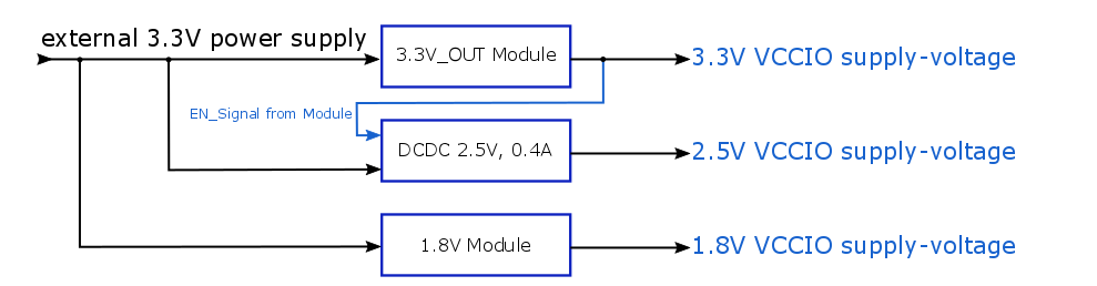
Figure 3: Power-On sequence diagram
...
| Date | Revision | Notes | PCN | Documentation link |
|---|---|---|---|---|
| - | 01 |
...
Figure 5: Hardware revision Number
...
Overview
Content Tools