Page History
...
Each conductor of the RX- and TX-LVDS-pair is routed to one coaxial connector:
| Connector designator | connected with | B2B |
|---|---|---|
| J5 | MGT_TX3_P | JM1-8 |
| J6 | MGT_TX3_N | JM1-10 |
| J7 | MGT_RX3_P | JM1-1 |
| J8 | MGT_RX3_N | JM1-3 |
Table 2: Pin-assignment of the coaxial connectors
...
The PL IO-bank supply-voltages 1.8V, 2.5V and 3.3V will be available powerd up after the mounted module's 3.3V voltage level is present has reached stable state on B2B-connector pin JM1-83, meaning that all on-module voltages have become stable and module is properly powered up.
Note: The supply-voltages have low current dropout.
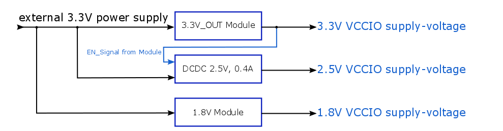
Figure 3: Power-On sequence diagram
...
On the TEBB0714 carrier board the PL IO-bank's supply voltages of the 4x5 SoM (VCCIOA, VCCIOD; see 4x5 Module Integration Guide) are connected to the base-board VCCIO-voltage VCCIOA and VCCIOD, which are voltage VCCIO34 is selectable between the supply-voltages 1.8V, 2.5V and 3.3V via jumper J26 and J27.
...
baseboard
supply-voltages
...
Table 5: base-board supply-voltages VCCIOA and VCCIOD
...
The
...
supply
...
Refer to SoM's schematic to get information about the specific pin-assignment on module's B2B-connectors regarding PL IO-bank supply-voltages and to the 4x5 Module integration Guide for VCCIO voltage options.
...
voltage VCCIO15 is routed on board to the pin '3.3V_OUT', hence it is fixed to 3.3V.
Following table describes how to configure the base-board supply-
...
voltage VCCIO34 by
...
jumper J26:
base-board supply- |
|---|
...
voltage |
|---|
...
...
| VCCIO34 |
|---|
...
| 1.8V | J26:1-2 |
...
| 2 |
...
| .5V | J26 |
...
| :3-4 | |
| 3.3V | J26 |
...
| : 5-6 |
Table 6: Configuration of base-board supply-voltages via jumpers. Jumper-Notification: 'Jx: 1-2' means pins 1 and 2 are connected, 'Jx: 3-4' means pins 3 and 4 are connected, and so on. Other pins are left open.
By jumper J27 the (depending on module's configuration: 3.3V or 1.8V)
Reference VCCIO JTAG Adapter | V_CFG |
|---|---|
| 1.8V | J27:1-2 |
| V_CGF0 | J27:3-4 |
| 3.3V_OUT | J27: 5-6 |
Table 7:
| Note |
|---|
| It is recommended to set and measure the PL IO-bank supply-voltages before mounting of TE 4x5 module to avoid failures and damages to the functionality of the mounted SoM. |
Technical Specifications
Absolute Maximum Ratings
...
Figure 4: Physical Dimensions of the TEBA0841TEBB0714-01 carrier board
Operating Temperature Ranges
...
| date | revision | authors | description |
|---|---|---|---|
| 2017-02-08 | Ali Naseri | current TRM for TEBA0841TEBB0714-01 | |
| 2017-01-30 | 0.1 | Ali Naseri | Initial document |
...
Overview
Content Tools