Page History
...
See page "4 x 5 cm carriers" to get information about the SoMs supported by the TE0701 Carrier Board.
Block Diagram
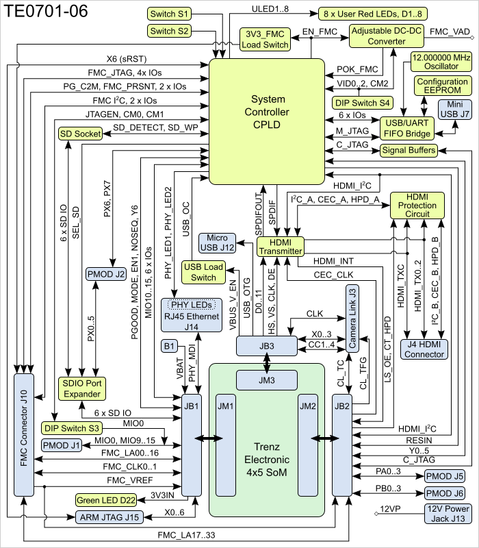
Figure 1: TE0701-06 Block Diagram
Main Components
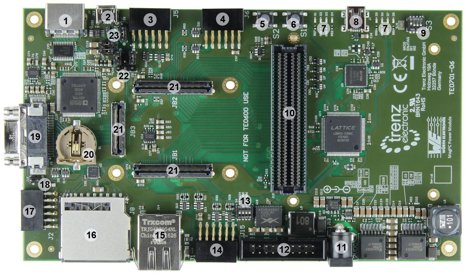
Figure 12: 4 x 5 SoM carrier board TE0701-06
...
The PL IO-bank supply voltage FMC_VADJ will be available after the output of the 5.0V-DCDC-converter is active and the pin EN_FMC of the SC-CPLD is asserted.
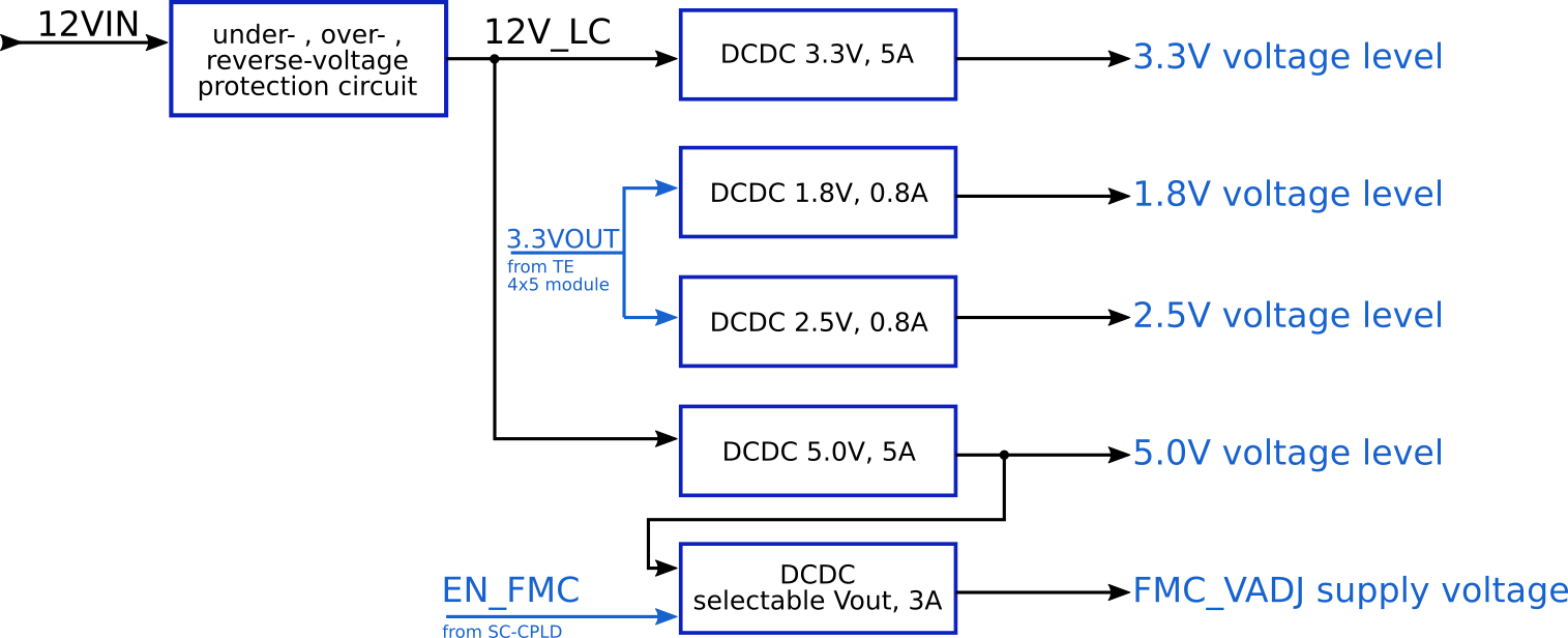
Figure 3: TE0701-06 Power-Up sequence diagram
TE0701 jumper and DIP switch overview
...
There are two base board supply-voltages VIOTA and VIOTB connected to the 4 x 5 SoM's PL IO-banks. The supply-voltages have following pin assignments on B2B-connectors:
...
Table 4: base-board supply-voltages VIOTA and VIOTB
...
All dimensions are given in mm.
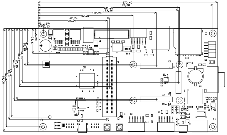
Figure 34: Physical Dimensions of the TE0701-06 carrier board
...
| date | revision | authors | description |
|---|---|---|---|
| 2017-04-11 | Ali Naseri | added block diagram | |
| 2017-02-15 | V45
| Ali Naseri | added warning concerning the use of FTDI-tools |
| 2017-02-15 | V40 | Ali Naseri | added power-on sequence diagram |
| 2017-01-19 | V35 | Ali Naseri | correction of table 3 (switch-positions to adjust FMC_VADJ) inserted hint to set and measure the PL IO-bank supply-voltages
|
| 2017-01-13 | V20 | Ali Naseri | added section for base-board supply- voltage configuration |
| 2016-11-29 | V10
| Ali Naseri | TRM update due to new revision 06 of the carrier board. |
| 2016-11-28 | V4 | Ali Naseri | TRM adjustment to the newest revision (05) of TE0701 Carrier Board. |
| 2014-02-18 | 0.2
| Sven-Ole Voigt | TE0701-03 (REV3) updated |
| 2014-01-05 | 0.1 | Sven-Ole Voigt | Initial release |
All |
...
| Date | Revision | Notes | PCN | Documentation link |
|---|---|---|---|---|
| - | 06 | additional Jumper J16 and switch S4 for setting VCCIO FMC_VADJ. | PCN-20161128 | |
| - | 05 | improved manufacturing | TRM-TE0701-05 | |
| - | 04 | |||
| - | 03 | changed DC/DC converters | ||
| - | 02 | Prototype | ||
| - | 01 | Prototype |
Figure 45: Hardware revision Number
...
Overview
Content Tools