Page History
...
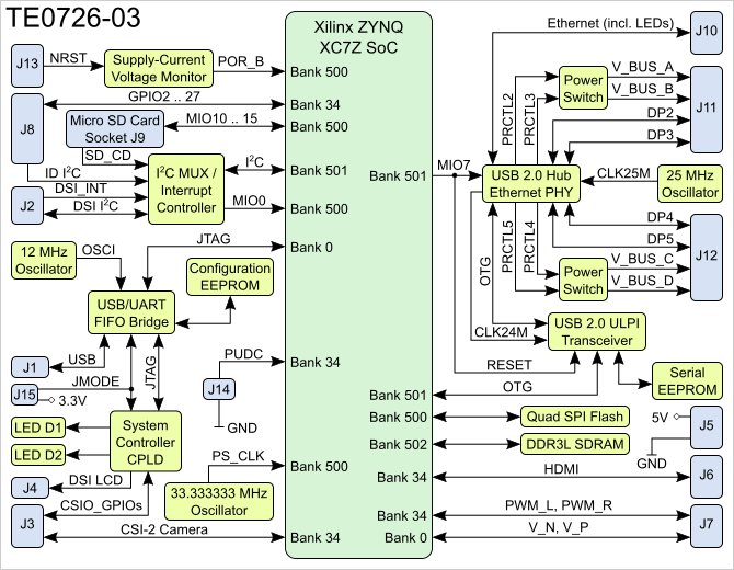
Block Diagram
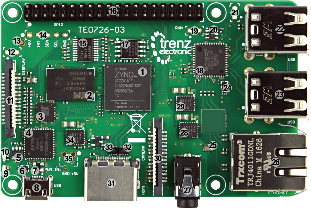
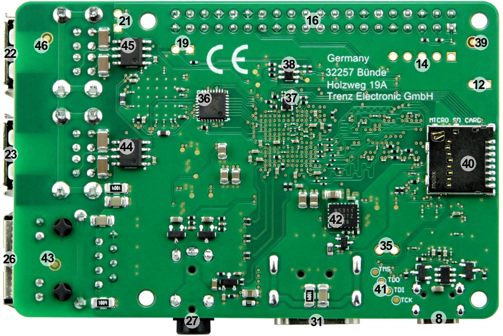
Main Components
- Xilinx Zynq XC7Z010 All Programmable SoC, U1
- 512 MByte DDR3L SDRAM, U8
- Lattice Semiconductor MachXO2 System Controller CPLD, U11
- Dual high-speed USB to multipurpose UART/FIFO, U3
- 2 Kbit Microwire compatible serial EEPROM, U6
- Low-power, programmable oscillator @ 12.000000 MHz, U7
- Ultra-low capacitance double rail-to-rail ESD protection diode ,U4
- Micro-USB 2.0 B receptacle, J1
- Green LED (GLED), D1
- Red LED (RLED), D2
- DSI LCD connector, J4
- JTAGENB, when low, TDO, TDI, TMS and TCK function as GPIOs, J15
- Fiducial mark PM2
- External I2C bus with interrupt signal and power line, J2
- Low-voltage 4-channel I2C and SMBus multiplexer with interrupt logic, U10
- 2x20 pin 2.54 GPIO header, J8
128 Mbit (16 MByte) 3.0V SPI Flash memory, U5
- USB 2.0 Hub and 10/100 Ethernet controller, U2
- External reset
- 2 Kbit Microwire compatible serial EEPROM, U9
- PUDC of Zynq, active low enables internal pull-ups during configuration on all SelectIO pins
- Dual USB A receptacle, J12. Also fiducial mark PM1
- Dual USB A receptacle, J11
- Low power programmable oscillator @ 25.000000 MHz, U13
- Molex’s miniature traceability S/N pad for low-cost, unique product identification
- RJ-45 Ethernet connector with 10/100 integrated magnetics, J10. Also fiducial mark PM3
- 3.5mm RCA audio jack, J7
- 1A PowerSoC synchronous buck regulator with integrated inductor (3.3V), U20
- 1A PowerSoC synchronous buck regulator with integrated inductor (1.8V), U19
- ZIF FFC/FPC CSI-2 camera connector, J3
- HDMI connector, J6
Common mode filter with ESD protection, D8
Common mode filter with ESD protection, D9
- 1A PowerSoC synchronous buck regulator with integrated inductor (1.35V), U16
- Additional external +5V power supply connector, J5
Highly integrated full featured hi-speed USB 2.0 ULPI transceiver, U18
- Low-power programmable oscillator @ 33.333333 MHz, U14
- Ultra-low supply current voltage monitor with optional watchdog, U22
- Fiducial mark PM4
- Micro SD memory card connector with detect switch, J9
- JTAG interface, TP1 (TDI), TP3 (TDO), TP5 (TCK), TP7 (TMS)
- 1A PowerSoC synchronous buck regulator with integrated inductor (1.0V), U17
- Fiducial mark PM6
- 0.5A dual channel current-limited power switch, U15
- 0.5A dual channel current-limited power switch, U21
- Fiducial mark PM5
...
FPGA IO Banks Pin Mapping
| Bank | Zynq Pin | Name | Connected To |
|---|---|---|---|
| 34 | G14 | PUDC | Jumper J14 |
| 35 | G15 | DSI_XA | System Controller CPLD, pin 16 |
| 35 | F15 | DSI_XB | System Controller CPLD, pin 17 |
Page break
GPIO to Header J8 Interface Mapping
...
| Parameter | Min | Max | Units | Notes |
|---|---|---|---|---|
| Power supply voltage | 2.7 | 5.5 | V | See AP2152SG-13 datasheet. |
| Operating temperature | 0 | 70 | °C | - |
The module operating temperature range depends on customer design and cooling solution. Please contact us for options.
Physical Dimensions
Module size: 40 mm × 30 mm. Please download the assembly diagram for exact numbers.
Mating height with standard connectors: 8 mm
PCB thickness: 1.6 mm
Highest part on PCB: approximately 2.5 mm. Please download the step model for exact numbers.
All dimensions are shown in millimeters. Additional sketches, drawings and schematics can be found here.
Operating Temperature Ranges
The module operating temperature range depends on customer design and cooling solution. Please contact us for options.
Commercial grade modules
All parts are at least commercial temperature range of 0 °C to +70 °C.
Industrial grade modules
All parts are at least industrial temperature range of -40 °C to +85 °C.
Weight
| Variant | Weight in g | Note |
|---|---|---|
| TE0726-03M | --- | Plain module. |
| TE0726-03R | --- | Plain module. |
| TE0726-03-07S-1C | --- | Plain module. |
...


