Page History
...
| MIO | Function | B2B Pin | Notes | MIO | Function | B2B Pin | Notes | |
|---|---|---|---|---|---|---|---|---|
| 0 | GPIO | JM1-87 | B2B | 16..27 | ETH0 | - | RGMII | |
| 1 | QSPI0 | - | SPI Flash-CS | 28..39 | USB0 | - | ULPI | |
| 2 | QSPI0 | - | SPI Flash-DQ0 | 40 | SDIO0 | JM1-27 | B2B | |
| 3 | QSPI0 | - | SPI Flash-DQ1 | 41 | SDIO0 | JM1-25 | B2B | |
| 4 | QSPI0 | - | SPI Flash-DQ2 | 42 | SDIO0 | JM1-23 | B2B | |
| 5 | QSPI0 | - | SPI Flash-DQ3 | 43 | SDIO0 | JM1-21 | B2B | |
| 6 | QSPI0 | - | SPI Flash-SCK | 44 | SDIO0 | JM1-19 | B2B | |
| 7 | GPIO | - | Green LED D4 | 45 | SDIO0 | JM1-17 | B2B | |
| 8 | QSPI0 | - | SPI Flash-SCKFB | 46 | GPIO | - | Ethernet PHY LED2 INTn Signal. | |
| 9 | JM1-91 | B2B | 47 | GPIO | - | RTC Interrupt | ||
| 10 | JM1-95 | B2B | 48 | I2C1 | - | SCL on-board I2C | ||
| 11 | JM1-93 | B2B | 49 | I2C1 | - | SDA on-board I2C | ||
| 12 | JM1-99 | B2B | 50 | GPIO | - | ETH0 Reset | ||
| 13 | JM1-97 | B2B | 51 | GPIO | - | USB Reset | ||
| 14 | UART0 | JM1-92 | B2B | 52 | ETH0 | - | MDC | |
| 15 | UART0 | JM1-85 | B2B | 53 | ETH0 | - | MDIO |
| Page break |
|---|
Gigabit Ethernet
On-board Gigabit Ethernet PHY is provided with Marvell Alaska 88E1512 IC (U7). The Ethernet PHY RGMII interface is connected to the Zynq Ethernet0 PS GEM0. I/O voltage is fixed at 1.8V for HSTL signalling. SGMII (SFP copper or fiber) can be used directly with the Ethernet PHY, as the SGMII pins are available on the B2B connector JM3. The reference clock input of the PHY is supplied from an on-board 25.000000 MHz oscillator (U9), the 125MHz output clock signal CLK_125MHZ is connected to the IN5 pin of the PLL chip (U10).
...
| PHY Pin | ZYNQ PS | ZYNQ PL | Notes |
|---|---|---|---|
| MDC/MDIO | MIO52, MIO53 | - | - |
| LED0 | - | J3 | Can be routed via PL to any free PL I/O pin in B2B connector. |
| LED1 | - | K8 | Can be routed via PL to any free PL I/O pin in B2B connector. This LED is connected to PL via level-shifter implemented in system controller CPLD. |
| LED2/Interrupt | MIO46 | - | - |
| CONFIG | - | - | By default the PHY address is strapped to 0x00, alternate configuration is possible. |
| RESETn | MIO50 | - | - |
| RGMII | MIO16..MIO27 | - | - |
| SGMII | - | - | Routed to B2B connector JM3. |
| MDI | - | - | Routed to B2B connector JM1. |
| Page break |
|---|
USB Interface
USB PHY is provided by USB3320 from Microchip. The ULPI interface is connected to the Zynq PS USB0. The I/O Voltage is fixed at 1.8V. The reference clock input of the PHY is supplied from an on-board 52.000000 000000 MHz oscillator (U15).
USB PHY connection
...
| Include Page | ||||
|---|---|---|---|---|
|
Technical Specifications
Absolute Maximum Ratings
Variants Currently in Production
| Module Variant | Zynq SoC | Temperature Range | B2B Connector Height |
|---|---|---|---|
| TE0715-04-15-1I | XC7Z015-1CLG485I | Industrial | 4.0 mm |
| TE0715-04-15-2I | XC7Z015-2CLG485I | Industrial | 4.0 mm |
| TE0715-04-30-1I | XC7Z030-1SBG485I | Industrial | 4.0 mm |
| TE0715-04-30-3E | XC7Z030-3SBG485E | Extended | 4.0 mm |
| TE0715-04-15-1I3 | XC7Z015-1CLG485I | Industrial | 2.5 mm |
| TE0715-04-30-1I3 | XC7Z030-1SBG485I | Industrial | 2.5 mm |
| TE0715-04-30-1C | XC7Z030-1SBG485C | Commercial | 4.0 mm |
Technical Specifications
Absolute Maximum Ratings
Parameter | Min | Max | Units | Notes |
|---|---|---|---|---|
VIN supply voltage | -0.3 | 6.0 | V | - |
3.3VIN supply voltage |
Parameter
Units
Notes
VIN supply voltage
-0.3
6.0
V
-0.4 | 3.6 | V | - | |
| VBAT supply voltage | -1 | 6.0 | V | - |
| PL IO bank supply voltage for HR I/O banks (VCCO) | -0.5 | 3.6 | V | - |
PL IO bank supply voltage for HP I/O banks (VCCO) | -0.5 | 2.0 | V | TE0715-xx-15 does not have HP banks. |
| I/O input voltage for HR I/O banks | -0.4 | VCCO |
| + 0.55 | V | - |
| I/O input voltage for HP I/O banks | -0.55 | VCCO |
| + 0.55 | V | TE0715-xx-15 does not have HP banks. | ||
| GT receiver (RXP/RXN) and transmitter (TXP/TXN) | -0.5 | 1.26 | V | - |
Voltage on module JTAG pins | -0.4 | VCCO_0 + 0.55 | V | VCCO_0 is 3.3V nominal. |
Storage temperature | -40 | +85 | °C | - |
| Storage temperature without the ISL12020MIRZ and 88E1512 | -55 | +100 | °C | - |
| Note |
|---|
| Assembly variants for higher storage temperature range are available on request. |
...
| Parameter | Min | Max | Units | Notes | Reference Document | ||||
|---|---|---|---|---|---|---|---|---|---|
| VIN supply voltage | 2.5 | 5.5 | V | ||||||
| 3.3VIN supply voltage | 3.135 | 3.465 | V | ||||||
| VBAT_IN supply voltage | 2.7 | 5.5 | V | ||||||
PL I/O bank supply voltage for HR I/O banks (VCCO) | 1.14 | 3.465 | V | Xilinx datasheet DS191 | |||||
PL I/O bank supply voltage for HP I/O banks (VCCO) | 1.14 | 1.89 | V | TE0715-xx-15 does not have HP banks | Xilinx datasheet DS191 | ||||
| I/O input voltage for HR I/O banks | (*) | (*) | V | (*) Check datasheet | Xilinx datasheet DS191 or DS187 | ||||
| I/O input voltage for HP I/O banks | (*) | (*) | V | TE0715-xx-15 does not have HP banks (*) Check datasheet | Xilinx datasheet DS191 | ||||
| Voltage on Module JTAG pins | 3.135 | 3.465 | V | VCCO_0 is 3.3 V nominal | 3.465 | V | VCCO_0 is 3.3 V nominal |
Operating Temperature Ranges
Commercial grade: 0°C to +70°C.
Industrial and extended grade: -40°C to +85°C.
The module operating temperature range depends also on customer design and cooling solution. Please contact us for options.
| Page break |
|---|
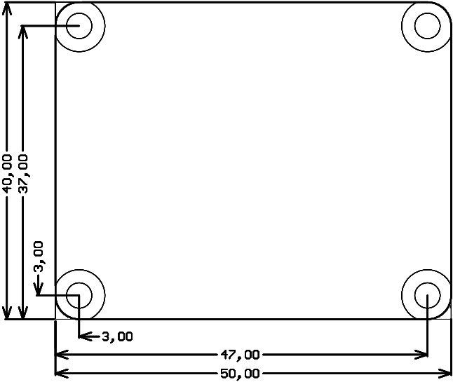
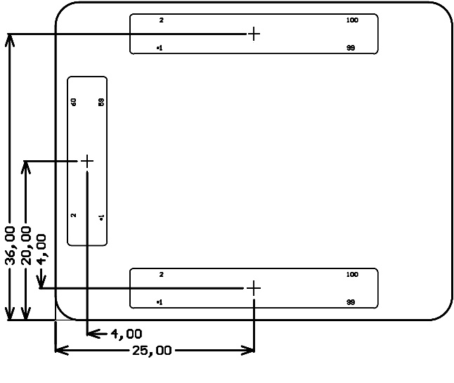
Physical Dimensions
...
All dimensions are given in millimeters.
Operating Temperature Ranges
Commercial grade: 0°C to +70°C.
Industrial grade: -40°C to +85°C.
The module operating temperature range depends also on customer design and cooling solution. Please contact us for options.
Weight
26 g - Plain module
8.8 g - Set of bolts and nuts
...
Overview
Content Tools