Page History
...
See "4 x 5 cm carriers" page for more information about supported 4 x 5 cm SoMs.
Block Diagram
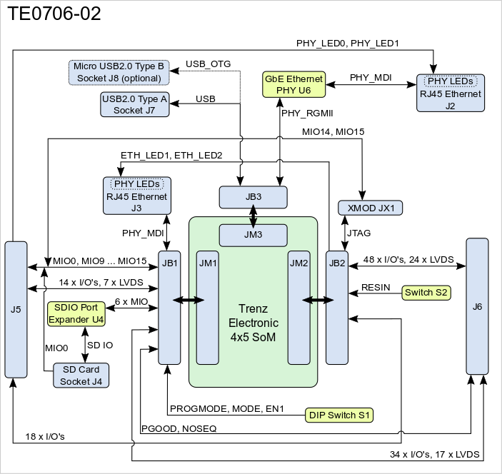
Main Components
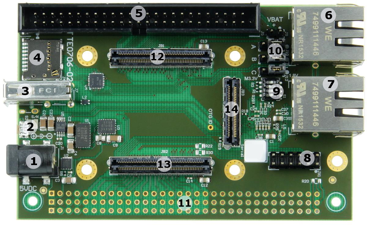
- 5V power connector jack, J1
- Reset switch, S2
- USB type A receptacle, J7
- Micro SD card socket with detect switch, J4
- 50 pin IDC male connector, J5
- 1000Base-T Gigabit RJ45 Ethernet MagJack, J3
- 1000Base-T Gigabit RJ45 Ethernet MagJack, J2
- JTAG/UART Connector, JX1
- User DIP switch block, S1
- VCCIO voltage selection jumper block, J10 - J12
- External connector (VG96) placeholder, J6
- Samtec Razor Beam™ LSHM-150 B2B connector, JB1
- Samtec Razor Beam™ LSHM-150 B2B connector, JB2
- Samtec Razor Beam™ LSHM-130 B2B connector, JB3
Key Features
- VG96 backplane connector (mounting holes and solder pads, J6) and 50-pin IDC male connector socket (J5) to access FPGA bank's IO-pins
- SDIO port expander with voltage-level translation
- Micro SD card socket, routed to B2B-connector JB1
- USB type A connector (OTG mode), routed to B2B-connecor JB3
- 1 x user-push button S2, routed to RESIN-pin on B2B-connector JB2. By default it is configured as system reset button.
- 1 x RJ45 Gigabit Ethernet MagJack J3, PHY_MDI interface routed to B2B-connector JB1.
- 1 x Marvell Alaska 88E1512 Ethernet PHY, routed to B2B-connector JB3 and accessible via RJ45 Gigabit Ethernet MagJack J2
- Barrel jack for 5 V Power Supply input
- 4 A High-Efficiency Power SoC DC-DC Step-Down Converter (Enpirion EN6347) for 3.3 V Power Supply
- Trenz 4 x 5 Module Socket (3 x Samtec LSHM series connectors)
- JTAG/UART-pins on 12-pin header JX1, routed to B2B-connector JB2
- user configurable DIP switch S1 to set System Controller CPLD signals on SoM
- 3 x VCCIO selection jumper J10, J11 and J12 to set SoM's bank voltages
Block Diagram
Main Components
- 5V power connector jack, J1
- Reset switch, S2
- USB type A receptacle, J7
- Micro SD card socket with detect switch, J4
- 50 pin IDC male connector, J5
- 1000Base-T Gigabit RJ45 Ethernet MagJack, J3
- 1000Base-T Gigabit RJ45 Ethernet MagJack, J2
- JTAG/UART Connector, JX1
- User DIP switch block, S1
- VCCIO voltage selection jumper block, J10 - J12
- External connector (VG96) placeholder, J6
- Samtec Razor Beam™ LSHM-150 B2B connector, JB1
- Samtec Razor Beam™ LSHM-150 B2B connector, JB2
- Samtec Razor Beam™ LSHM-130 B2B connector, JB3
Initial Delivery State
Board is shipped in following configuration:
...
| Info |
|---|
| Note: Pin OTG-ID is only assigned to USB 2.0 type B socket. |
DIP switch S1
| Switch | Signal Name | ON | OFF | Notes |
|---|---|---|---|---|
| S1-1 | - | - | - | Not connected |
| S1-2 | PROGMODE | JTAG enabled for programing SoM FPGA | JTAG enabled for programing SoM CPLD | - |
| S1-3 | MODE | Drive SoM SC CPLD pin 'MODE' low | leave SoM SC CPLD pin 'MODE' open | Boot mode configuration, if supported by SoM. (Depends also on SoM's SC CPLD firmware). |
| S1-4 | EN1 | Drive SoM SC CPLD pin 'EN1' low | drive SoM SC CPLD pin 'EN1' high | Usually used to enable/disable FPGA core-voltage supply. (Depends also on SoM's SC CPLD firmware). Note: Power-on sequence will be intermitted when S1-4 is set to OFF and functionality is supported by SoM. |
Connector J5 and J6
On the TE0706-02 carrier board there is one 50-pin IDC male connector socket available for access to the SoM's PL IO-bank-pins. 32 module's IO-pins are also usable as 18 LVDS-pairs and 8 IO's as single-ended (MIO0, MIO9 - MIO 15), which give access to the MIO0-bank of the Zynq-module if mounted. The available VCCIOs on this connector are 3.3V and M3.3VOUT from module. This connector gives also access to the LEDs of MagJack J2.
...
Following table shows how to configure the voltage-levels of base-board supply-voltages VCCIOA, VCCIOB and VCCIOC by jumper, 0-Ohm-resistor or by feeding the supply voltage through connector J6:
| Supply Voltage by Jumper | Supply Voltage by 0-Ohm Resistor | Supply Voltage by Connector J6 | ||||
|---|---|---|---|---|---|---|
| Voltage Level | 1.8V | 3.3V | 1.8V | 3.3V | Variable | |
| VCCIOA | J10: 1-2, 3 | J10: 1, 2-3 | - | R20 | J6 pin B32 | |
| VCCIOB | J11: 1-2, 3 | J11: 1, 2-3 | R29 | R21 | - | |
| VCCIOC | J12: 1-2, 3 | J12: 1, 2-3 | R30 | R22 | J6 pin B1 | |
Jumper-Notification: 'Jx: 1-2, 3' means pins 1 and 2 are connected, 3 is open. 'Jx: 1, 2-3' means pins 2 and 3 are connected, 1 is open.
...
Technical Specifications
Absolute Maximum Ratings
Parameter | Min | Max | Units | Reference document |
|---|---|---|---|---|
Supply voltage VIN |
4. |
75 |
| 5.25 | V | EN6347QI / EN5311QI datasheet. Note: USB-VBUS = VIN, if enabled. | ||
Storage temperature | -55 | +125 | °C | Marvell 88E1512 datasheet. |
Recommended Operating Conditions
Parameter | Min | Max | Units | Reference document |
|---|---|---|---|---|
Supply Voltage Vin | 4.75 | 5.25 | V | - |
| Operating temperature | 0 | +70 | °C | Commercial grade. |
| Note |
|---|
| Please check components datasheets for complete list of absolute maximum and recommended operating ratings. |
...
Hardware revision number is printed on the PCB board next to the module model number separated by the dash.
Document Change History
Date | Revision | Contributors | Description |
|---|---|---|---|
| 2017-01-19 | Ali Naseri, Jan Kumann | Hardware revision 02 specific changes. | |
| 2016-01-06 | V1 | Ali Naseri | Initial document. |
Disclaimer
| Include Page | ||||
|---|---|---|---|---|
|
Overview
Content Tools