Page History
...
The Trenz Electronic TE0706 carrier board provides functionality for testing, evaluation and development purposes of company's 4 x 5 cm SoMs (System on Module). The Carrier board is equipped with various components and connectors for different configuration setups and needs. On-module functional components and multipurpose I/Os of the SoM's PL logic are connected via board-to-board connectors to the carrier board's components and connectors for easy user access.
...
- 5V power connector jack, J1
- Reset switch, S2
- USB type A receptacle, J7
- Micro SD card socket with detect switchCard Detect, J4
- 50 pin IDC male connector, J5
- 1000Base-T Gigabit RJ45 Ethernet MagJack, J3
- 1000Base-T Gigabit RJ45 Ethernet MagJack, J2
- JTAG/UART Connector, JX1
- User DIP switch block, S1
- VCCIO voltage selection jumper block, J10 - J12
- External connector (VG96) placeholder, J6
- Samtec Razor Beam™ LSHM-150 B2B connector, JB1
- Samtec Razor Beam™ LSHM-150 B2B connector, JB2
- Samtec Razor Beam™ LSHM-130 B2B connector, JB3
...
JTAG/UART Interface
JTAG access to the mounted 4 x 5 SoM is provided via 12-pin header JX1 and controlled by DIP switch S1-2 to select the device (Zynq-SoC, SC-CPLD) to program. JTAG pins are routed to the JB2 and JX1 connectors as follows:
This header has a 'XMOD FTDI JTAG Adapter'-compatible pin-assignment, so the XMOD-FT2232H adapter-board TE0790 can be used in conjunction with the carried board to program the mounted SoM via USB interface.
| JX1 pin | Configured as | B2B |
|---|---|---|
| C (pin 4) | TCK | JB2-100 |
| D (pin 8) |
JTAG Signal
B2B Connector
| TDO | JB2-98 |
| F (pin 10) | TDI | JB2-96 |
| H (pin 12) | TMS |
| JB2- |
On connector JX1 there also two pins available, which can be used as RX-/TX-lane for UART:
| 94 | ||
| A (pin 3) | MIO15 | JB1-86 (usable as UART RX/TX-line) |
| B (pin 7) |
| MIO14 | JB1-91 (usable as UART RX/TX-line) |
Micro SD Card Socket
Micro SD Card socket is not directly wired to the B2B connector pins, but routed through a Texas Instruments TXS02612 SDIO port expander, which is needed for voltage translation due to the different voltage levels of the Micro SD Card and MIO bank 501 of the Xilinx Zynq 7000 chip. The Micro SD Card has 3.3 V signal voltage-level, but the MIO Bank 501 on the Xilinx Zynq 7000 chip is set to 1.8 V.
...
| Switch | Signal Name | ON | OFF | Notes |
|---|---|---|---|---|
| S1-1 | - | - | - | Not connected. |
| S1-2 | PROGMODE | JTAG enabled for programing SoM FPGA's Zynq-SoC. | JTAG enabled for programing SoM CPLDSoM's CPLD. | - |
| S1-3 | MODE | Drive SoM SC CPLD pin 'MODE' low. | leave Leave SoM SC CPLD pin 'MODE' open. | Boot mode configuration, if supported by SoM. (Depends also on SoM's SC CPLD firmware). |
| S1-4 | EN1 | Drive SoM SC CPLD pin 'EN1' low. | drive Drive SoM SC CPLD pin 'EN1' high. | Usually used to enable/disable FPGA core-voltage supply. (Depends also on SoM's SC CPLD firmware). Note: Power-on sequence will be intermitted when S1-4 is set to OFF and functionality is supported by SoM. |
...
Place-holder J6 provides the possibility to mount and solder a VG96 backplane connector te get access to SoM's PL IO-bank-pins. 82 IO's are available on this connector, which are also usable as up to 41 LVDS-pairs. The available VCCIOs on this connector are 3.3V and M3.3VOUT from module and also the selectable PL I/O bank supply-voltages VCCIOA and VCCIOC. The pins A1, A2 are connected to the barrel jack for 5 V Power supply input.
On the TE0706-02 carrier board there is one 50-pin IDC male connector socket and a place-holder (VG96-Connector solder pads) J6 to provides access to SoM's PL IO-bank-pins. With this user interfaces, a large quantity of IO's are also usable as LVDS-pairs and different VCCIO's are available to operate the IO's properly.
Following table gives a summary of the optional pin-headers of the base-board:
| Connector Designator | Connector Type | Count of IO's | Count of LVDS Pairs | Available VCCIO's | Interfaces |
|---|---|---|---|---|---|
| J5 | 50-pin IDC male | 40 | 16 | 3.3V, | access to the LEDs of MagJack J2 |
| J6 | VG96-Connector | 82 | 41 | 3.3V, | PGOOD-, NOSEQ-Signal of SC-CPLD of mounted 4 x 5 SoM |
Power and Power-On Sequence
...
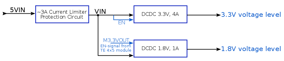
It is not allowed to feed any voltage to any external I/O pin before there is no power indication on M3.3VOUT pins. Presence of 3.3V on B2B JB2 connector pins 9 and 11 indicates that module is properly powered up and ready. The 1.8V voltage-level on base-board for supplying PL I/O bank supply-voltages will be powered up after the module's 3.3V voltage-level has reached stable state and M3.3VOUT is available on the B2B-connector JB2, pins 9 and 11.
If VCCIOA or VCCIOC will be powered through the dedicated pins of external connector J6, then corresponding VCCIO jumpers J10 and J12 should be removed.
...
Absolute Maximum Ratings
Parameter | Min | Max | Units | Reference documentNote |
|---|---|---|---|---|
Supply voltage VIN | 4.75 | 5.25 | V | EN6347QI / EN5311QI datasheet.TPS2051DGN power distribution switch Note: USB-VBUS = VIN, if enabled. |
Storage temperature | -55 | +125 | °C | Marvell 88E1512 datasheet. |
Recommended Operating Conditions
Parameter | Min | Max | Units | Reference documentNote |
|---|---|---|---|---|
Supply Voltage Vin | 4.75 | 5.25 | V | - |
| Operating temperature | 0 | +70 | °C | Commercial grade. |
...
Overview
Content Tools