Page History
...
This base-board provides also soldering-pads as place-holders for pin-headers as option to get access to the PL-IO-banks of the mounted SoM.
Key Features
- SFP+ connector (Enhanced small form-factor pluggable), supports data transmission rates up to 10 Gbit/s
- 4 Hirose Ultra small SMT coaxial connectors, supports data transmission rates up to 6 Gbit/s
- TE 4 x 5 cm SoM programable by JTAG header (JX1)
- 2 x user LEDs routed to IO-pins of the SoM
- Soldering-pads J17 and J20 for optional pin headers for access to SoM's IO-bank-pins, usable as LVDS-pairs
- Soldering-pads J3 and J4 for optional pin headers for access to further interfaces and IO's of the SoM
Block Diagram
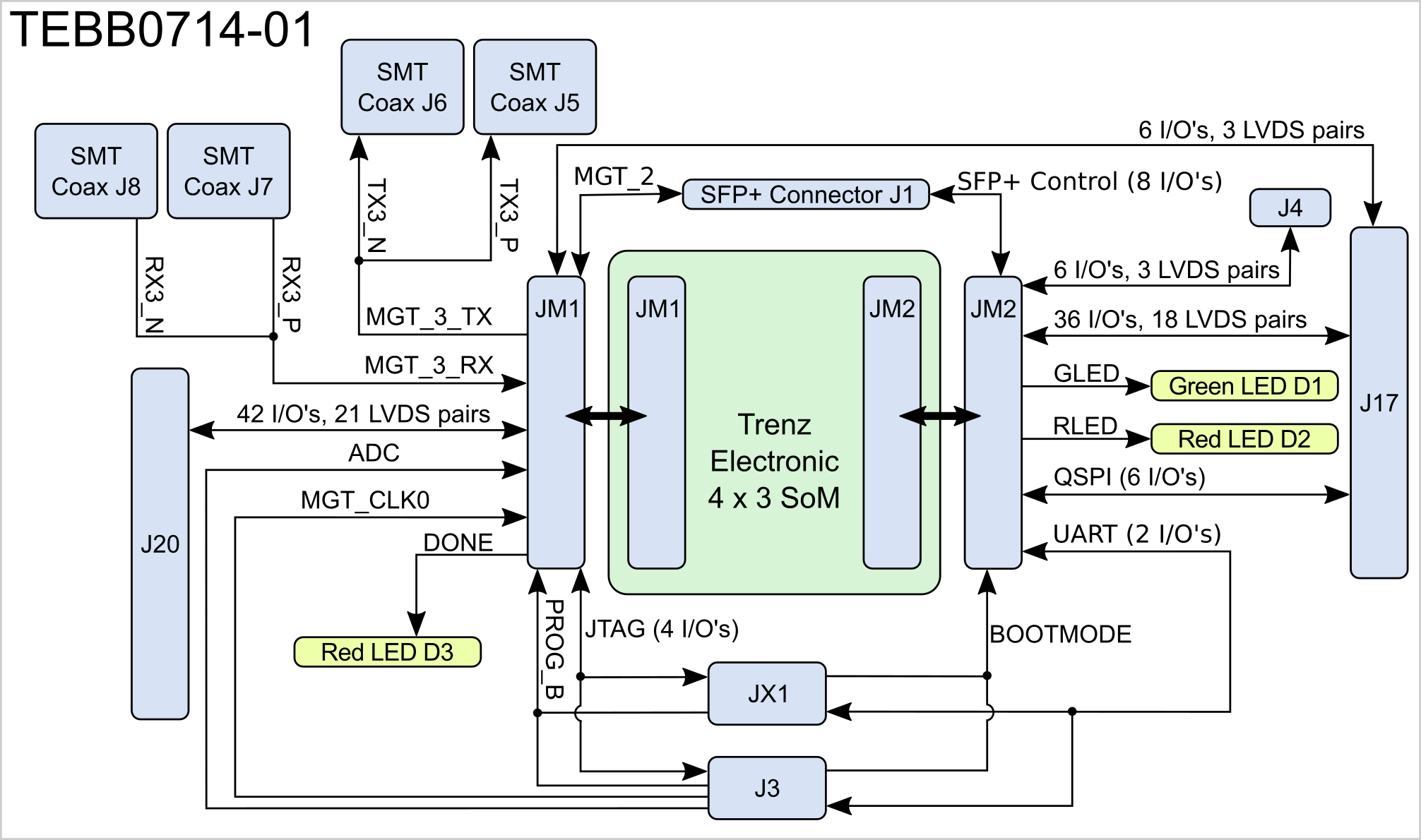
Figure 1: TEBB0714 -01 Block Diagram
...
- 6-pin header J26 for selecting Bank34 VCCIO voltage
- 6-pin header J27 for selecting XMOD/JTAG reference voltage
- Samtec Razor Beam™ LSHM-150 B2B connector JM1
- Samtec Razor Beam™ LSHM-150 B2B connector JM2
- JTAG/UART header JX1 ('XMOD FTDI JTAG Adapter'-compatible pin-assignment)
- Ultra small SMT coaxial connector J5
- Ultra small SMT coaxial connector J6
- Ultra small SMT coaxial connector J7
- Ultra small SMT coaxial connector J8
- User LED D1 (green)
- User LED D2 (red)
- LED D3 (red) indicating 'Programming DONE'-signal from module's FPGA
- SFP+ Connector J1
- 10-pin header soldering-pads J4 for access to SoM's PL IO-banks (LVDS-pairs possible)
- 16-pin header soldering-pads J3, JTAG/UART header ('XMOD FTDI JTAG Adapter'-compatible pin-assignment)
- 50-pin header soldering-pads J20 for access to SoM's PL IO-banks (LVDS-pairs possible)
- 50-pin header soldering-pads J17 for access to SoM's PL IO-banks (LVDS-pairs possible)
Key Features
...
- )
...
Interfaces and Pins
SFP+ Connector
...
The JTAG-interface of the mounted 4 x 5 SoM can be accessed via the headers header JX1 or J3 with 4 two additional pins for reference-clock input to (15,16) as LVDS-pair to supply the mounted 4 x 5 cm SoM and one LVDS-pair for analog signal inputSoM with an external reference clock-signal.
This headers have header has a 'XMOD FTDI JTAG Adapter'-compatible pin-assignment:, so the XMOD-FT2232H adapter-board TE0790 can be used in conjunction with the carried board to program the mounted SoM via USB interface.
| JX1 pin | JX1 pin net-name | B2B | J3 pin | J3 pin net-name | B2B | |
|---|---|---|---|---|---|---|
| C (pin 4) | TCK | JM1-90 | 4 | TCK | JM1-90 | |
| D (pin 8) | TDO | JM1-88 | 8 | TDO | JM1-88 | |
| F (pin 10) | TDI | JM1-86 | 10 | TDI | JM1-86 | |
| H (pin 12) | TMS | JM1-92 | 12 | TMS | JM1-92 | |
| A (pin 3) | B14_L25 (usable as UART RX/TX-line) | JM2-97 | 3 | B14_L25 | JM2-97 (usable as UART RX/TX-line) | |
| B (pin 7) | B14_L0 (usable as UART RX/TX-line) | JM2-99 | 7 | B14_L0 | JM2-99 (usable as UART RX/TX-line) | |
| E (pin 9) | BOOTMODE | JM2-100 | 9 | BOOTMODE | JM2-100 | |
| G (pin 11) | PROG_B | JM1-94 | 11 | PROG_B | JM1-94 | |
| - | - | - | 13 | XADC_P | JM1-25 (ADC_P, decoupling capacitator 100 nF) | |
| - | - | - | 14 | XADC_N | JM1-27 (ADC_N, decoupling capacitator 100 nF) | |
| - | - | - | 15 | CLK0_P | JM1-2 (MGT_CLK0_P, 1KΩ serial resistor) | |
| - | - | - | 16 | CLK0_N | JM1-4 (MGT_CLK0_N, 1KΩ serial resistor) |
Table 3: JTAG/UART header JX1 / J3 pin-assignment
...
| Note |
|---|
| It is recommended to set and measure the PL IO-bank supply-voltages before mounting of TE 4x5 module to avoid failures and damages to the functionality of the mounted SoM. |
Technical Specifications
Absolute Maximum Ratings
...
| Include Page | ||||
|---|---|---|---|---|
|
Overview
Content Tools